EP0216352A2 - Semiconductor element sealing structure - Google Patents
Semiconductor element sealing structure Download PDFInfo
- Publication number
- EP0216352A2 EP0216352A2 EP86113076A EP86113076A EP0216352A2 EP 0216352 A2 EP0216352 A2 EP 0216352A2 EP 86113076 A EP86113076 A EP 86113076A EP 86113076 A EP86113076 A EP 86113076A EP 0216352 A2 EP0216352 A2 EP 0216352A2
- Authority
- EP
- European Patent Office
- Prior art keywords
- semiconductor element
- substrate
- silicone gel
- elasticity
- structure according
- Prior art date
- Legal status (The legal status is an assumption and is not a legal conclusion. Google has not performed a legal analysis and makes no representation as to the accuracy of the status listed.)
- Granted
Links
Images


Classifications
-
- H—ELECTRICITY
- H01—ELECTRIC ELEMENTS
- H01L—SEMICONDUCTOR DEVICES NOT COVERED BY CLASS H10
- H01L24/00—Arrangements for connecting or disconnecting semiconductor or solid-state bodies; Methods or apparatus related thereto
- H01L24/80—Methods for connecting semiconductor or other solid state bodies using means for bonding being attached to, or being formed on, the surface to be connected
- H01L24/81—Methods for connecting semiconductor or other solid state bodies using means for bonding being attached to, or being formed on, the surface to be connected using a bump connector
-
- H—ELECTRICITY
- H01—ELECTRIC ELEMENTS
- H01L—SEMICONDUCTOR DEVICES NOT COVERED BY CLASS H10
- H01L23/00—Details of semiconductor or other solid state devices
- H01L23/16—Fillings or auxiliary members in containers or encapsulations, e.g. centering rings
- H01L23/18—Fillings characterised by the material, its physical or chemical properties, or its arrangement within the complete device
- H01L23/24—Fillings characterised by the material, its physical or chemical properties, or its arrangement within the complete device solid or gel at the normal operating temperature of the device
-
- H—ELECTRICITY
- H01—ELECTRIC ELEMENTS
- H01L—SEMICONDUCTOR DEVICES NOT COVERED BY CLASS H10
- H01L2224/00—Indexing scheme for arrangements for connecting or disconnecting semiconductor or solid-state bodies and methods related thereto as covered by H01L24/00
- H01L2224/80—Methods for connecting semiconductor or other solid state bodies using means for bonding being attached to, or being formed on, the surface to be connected
- H01L2224/81—Methods for connecting semiconductor or other solid state bodies using means for bonding being attached to, or being formed on, the surface to be connected using a bump connector
- H01L2224/818—Bonding techniques
- H01L2224/81801—Soldering or alloying
-
- H—ELECTRICITY
- H01—ELECTRIC ELEMENTS
- H01L—SEMICONDUCTOR DEVICES NOT COVERED BY CLASS H10
- H01L2924/00—Indexing scheme for arrangements or methods for connecting or disconnecting semiconductor or solid-state bodies as covered by H01L24/00
- H01L2924/01—Chemical elements
- H01L2924/01005—Boron [B]
-
- H—ELECTRICITY
- H01—ELECTRIC ELEMENTS
- H01L—SEMICONDUCTOR DEVICES NOT COVERED BY CLASS H10
- H01L2924/00—Indexing scheme for arrangements or methods for connecting or disconnecting semiconductor or solid-state bodies as covered by H01L24/00
- H01L2924/01—Chemical elements
- H01L2924/01006—Carbon [C]
-
- H—ELECTRICITY
- H01—ELECTRIC ELEMENTS
- H01L—SEMICONDUCTOR DEVICES NOT COVERED BY CLASS H10
- H01L2924/00—Indexing scheme for arrangements or methods for connecting or disconnecting semiconductor or solid-state bodies as covered by H01L24/00
- H01L2924/01—Chemical elements
- H01L2924/01019—Potassium [K]
-
- H—ELECTRICITY
- H01—ELECTRIC ELEMENTS
- H01L—SEMICONDUCTOR DEVICES NOT COVERED BY CLASS H10
- H01L2924/00—Indexing scheme for arrangements or methods for connecting or disconnecting semiconductor or solid-state bodies as covered by H01L24/00
- H01L2924/01—Chemical elements
- H01L2924/01033—Arsenic [As]
-
- H—ELECTRICITY
- H01—ELECTRIC ELEMENTS
- H01L—SEMICONDUCTOR DEVICES NOT COVERED BY CLASS H10
- H01L2924/00—Indexing scheme for arrangements or methods for connecting or disconnecting semiconductor or solid-state bodies as covered by H01L24/00
- H01L2924/01—Chemical elements
- H01L2924/01078—Platinum [Pt]
-
- H—ELECTRICITY
- H01—ELECTRIC ELEMENTS
- H01L—SEMICONDUCTOR DEVICES NOT COVERED BY CLASS H10
- H01L2924/00—Indexing scheme for arrangements or methods for connecting or disconnecting semiconductor or solid-state bodies as covered by H01L24/00
- H01L2924/013—Alloys
- H01L2924/014—Solder alloys
-
- H—ELECTRICITY
- H01—ELECTRIC ELEMENTS
- H01L—SEMICONDUCTOR DEVICES NOT COVERED BY CLASS H10
- H01L2924/00—Indexing scheme for arrangements or methods for connecting or disconnecting semiconductor or solid-state bodies as covered by H01L24/00
- H01L2924/10—Details of semiconductor or other solid state devices to be connected
- H01L2924/11—Device type
- H01L2924/14—Integrated circuits
-
- H—ELECTRICITY
- H01—ELECTRIC ELEMENTS
- H01L—SEMICONDUCTOR DEVICES NOT COVERED BY CLASS H10
- H01L2924/00—Indexing scheme for arrangements or methods for connecting or disconnecting semiconductor or solid-state bodies as covered by H01L24/00
- H01L2924/15—Details of package parts other than the semiconductor or other solid state devices to be connected
- H01L2924/161—Cap
- H01L2924/1615—Shape
- H01L2924/16195—Flat cap [not enclosing an internal cavity]
-
- H—ELECTRICITY
- H01—ELECTRIC ELEMENTS
- H01L—SEMICONDUCTOR DEVICES NOT COVERED BY CLASS H10
- H01L2924/00—Indexing scheme for arrangements or methods for connecting or disconnecting semiconductor or solid-state bodies as covered by H01L24/00
- H01L2924/15—Details of package parts other than the semiconductor or other solid state devices to be connected
- H01L2924/181—Encapsulation
-
- H—ELECTRICITY
- H01—ELECTRIC ELEMENTS
- H01L—SEMICONDUCTOR DEVICES NOT COVERED BY CLASS H10
- H01L2924/00—Indexing scheme for arrangements or methods for connecting or disconnecting semiconductor or solid-state bodies as covered by H01L24/00
- H01L2924/30—Technical effects
- H01L2924/35—Mechanical effects
- H01L2924/351—Thermal stress
-
- Y—GENERAL TAGGING OF NEW TECHNOLOGICAL DEVELOPMENTS; GENERAL TAGGING OF CROSS-SECTIONAL TECHNOLOGIES SPANNING OVER SEVERAL SECTIONS OF THE IPC; TECHNICAL SUBJECTS COVERED BY FORMER USPC CROSS-REFERENCE ART COLLECTIONS [XRACs] AND DIGESTS
- Y10—TECHNICAL SUBJECTS COVERED BY FORMER USPC
- Y10T—TECHNICAL SUBJECTS COVERED BY FORMER US CLASSIFICATION
- Y10T428/00—Stock material or miscellaneous articles
- Y10T428/31504—Composite [nonstructural laminate]
- Y10T428/31511—Of epoxy ether
-
- Y—GENERAL TAGGING OF NEW TECHNOLOGICAL DEVELOPMENTS; GENERAL TAGGING OF CROSS-SECTIONAL TECHNOLOGIES SPANNING OVER SEVERAL SECTIONS OF THE IPC; TECHNICAL SUBJECTS COVERED BY FORMER USPC CROSS-REFERENCE ART COLLECTIONS [XRACs] AND DIGESTS
- Y10—TECHNICAL SUBJECTS COVERED BY FORMER USPC
- Y10T—TECHNICAL SUBJECTS COVERED BY FORMER US CLASSIFICATION
- Y10T428/00—Stock material or miscellaneous articles
- Y10T428/31504—Composite [nonstructural laminate]
- Y10T428/31652—Of asbestos
- Y10T428/31663—As siloxane, silicone or silane
Definitions
- the present invention relates to a semiconductor element sealing structure used mainly for sealing a semiconductor element such as a flip-chip mounted on a hybrid substrate, to prevent breakage of the chip or chip connecting portion and to allow an increase of the size of the chip.
- a semiconductor chip is sealed with silicone gel or the like to electrically insulate and protect the chip from environmental hazards such as water, shock, and vibration.
- a flip-chip for example, is mounted on a conductor pattern formed on a thick layer printed substrate with soldering bumps formed on a main surface of the flip-chip.
- the flip-chip and the substrate are packed with silicone gel.
- the silicone gel entering a space between the flip-chip and the printed substrate is thermally expanded by the effect of the ambient temperature and self-generation of heat by various elements on the printed substrate, to pull up the flip-chip, and finally result in a breakage of the soldering bumps. We found that this phenomenon becomes more important as the size of a chip is increased, since the force pushing up the chip becomes larger.
- silicone gels used for the above purpose contain unreacted vinyl groups and such vinyl groups will cause additional reactions with some ingredients of another addition reaction type silicone adhesive, for example, an adhesive used for adhering a cap to a case in which the chip has been sealed, and form additional cross linkages in the sealing silicone gel or increase the cross linkage density, thereby increasing the hardness of the silicone gel and thus accelerating the action of pushing up the chip.
- silicone gels in which the hardness of the silicone gel will not change over a period of time, and in which the additional cross linking reaction of unreacted vinyl groups is improved have been proposed.
- silicone gels have a high original hardness and thus increase the force pushing up the chip, resulting in cracks or breakage of the flip-chips or breakage of the sodering bumps. Accordingly, these silicone gels limit the size of a chip which can be used.
- the object of the present invention is to eliminate the above described problems of the prior art and to provide a sealing structure in which a semiconductor element is sealed with a silicone gel and which prevents breakage of the semiconductor element or soldering bumps and allows an increase in the size of the element used.
- a semiconductor element sealing structure comprising: a) a semiconductor element having electrodes on a main surface thereof; b) a substrate having conductive members formed on the substrate, the semiconductor element being mounted on the substrate by bonding the electrodes to the conductive members with soldering bumps; and c) an addition reaction type silicone gel sealing at least the semiconductor element and existing also between the semiconductor element and the substrate.
- This silicone gel has: i) a complex modulus of elasticity lower than a specified value so that breakage of the bumps due to thermal fatigue occurs preferentially by shear stress theron due to a difference between the thermal expansion coefficients of the semiconductor element and the substrate, not by tension thereto due to thermal expansion of the silicone gel between the semiconductor element and the substrate; and preferably, ii) a ratio of free vinyl groups to ethylene groups lower than a specified value so that an increased complex modulus of elasticity of the silicone gel after the free vinyl groups have been used to form cross linkages is still lower than the above-defined specific value of the complex modulus of elasticity.
- the present invention resides in the finding that the pushing-up stress on the semiconductor element due to thermal expansion of a silicone gel has a close relationship with the complex modulus of elasticity of the silicone gel used, and the breakage of a semiconductor element or soldering bumps, even in an element having a large size, can be prevented by reducing the complex modulus of elasticity of a silicone gel below a specific value.
- This specific value is defined above and has a specified value valid if a specific semiconductor element is mounted onto a specific substrate with specific soldering bumps and if a temperature range in which the above specified structure is to be used is given.
- the complex modulus of elasticity of a silicone gel is so low that bumps are broken by repeated shear stress due to the difference between thermal expansion coefficients of a semiconductor element and a substrate, not by repeated tension due to thermal expansion of a silicone gel between the semiconductor element and the substrate.
- soldering bumps or a semiconductor element are broken due to repeated thermal expansion of a silicone gel between the semiconductor element and a substrate, but the life-time of the sealing structure is satisfactory because the size of a semiconductor element is relatively small, such as 3 mm square or so, so that soldering bumps or a semiconductor element are not broken due to repeated thermal expansion of a silicone gel prior to damage or breakage of a semiconductor element, per se, due to causes other than a repeated thermal expansion of a silicone gel.
- the size of a semiconductor element is increased, soldering bumps or a semiconductor element may be easily broken due to repeated thermal expansion of a silicone gel prior to damage or breakage of a semiconductor element for other reasons.
- reduction of the repeated tension due to thermal expansion of a silicone gel becomes necessary in a sealing structure using a relatively large semiconductor element.
- a silicone gel sealing a semiconductor element must not contain too large an amount of free or unreacted vinyl groups. This is to prevent an increase of the complex modulus of elasticity of a silicone gel over the above-defined upper limit after the free or unreacted vinyl groups have reacted, after time has lapsed, with some other addition reaction type material and so the silicone gel becomes harder or the complex modulus of elasticity thereof is increased.
- the increase of the complex modulus of elasticity of an addition reaction type silicone gel depends on the ratio of free or unreacted vinyl groups to ethylene groups. Therefore, by reducing the ratio of free or unreacted vinyl groups to ethylene groups, the over-increase of the complex modulus of elasticity of a silicone gel can be prevented.
- a silicone resin in the form of gel is used as an addition reaction type material for sealing a semiconductor element.
- Figure I shows a general structure of a hydrid IC to which the present invention is applied.
- reference number I denotes a flip-chip IC on a main surface of which soldering bumps 3 are formed
- reference numeral 2 denotes a thick layer circuit board on which a predetermined conductor pattern 2A is formed, the flip-chip IC I being soldered to a given portion of the conductor pattern 2A.
- Reference numeral 4 denotes a silicone gel as a sealing material, 5 a case made of a resin or metal, 6 an addition reaction type silicone adhesive, 7 a cap made of a resin or metal, 8 a space of air or resin, and 9 a gap between the flip-chip IC I and the circuit board 2 wherein the silicone gel 4 is filled.
- this thermal strain comprises shear strain 5 s produced by a difference between thermal expansion coefficients of the flip-chip IC I and the circuit board 2, as well as tensile strain ⁇ E produced by thermal expansion of the silicone gel 4 inserted into the gap having the height of the bumps 3 between the flip-chip IC I and the circuit board 2, to push up the flip-chip IC 1.
- the shear strain 5 s and the tensile strain ⁇ E increase with the increase of the chip size of the flip-chip IC I.
- the strain which causes cracking of the flip-chip IC I or breakage of the soldering bumps 3 is the tensile strain ⁇ E .
- the first mode of breakage of the soldering bumps 3 occurs due to pushing-up the flip-chip IC I by thermal expansion of the silicone gel 4 directly below the flip-chip IC I. This is true even when the flip-chip IC I has a small chip size in a sealing structure in the prior art, as described before.
- the force from the silicone gel 4 pushing up the chip I is reduced in such a way that breakage due to the shear strain 5 s appears prior to breakage due to the tensile strain ⁇ E . Accordingly, enlargement of the chip I and extension of the thermal fatique life of the soldering bumps 3 due to repeated temperature cycles can be attained, and as a result, higher and-multiplied functions can be attained in a single chip and the reliability of the whole device involving the sealing structure can be increased.
- a gel 4 is charged between a plate II and a cone 12 of a measuring unit 10 and heat cured under a standard curing condition for the gel and then cooled to 30°C.
- the plate II is then vibrated at an amplitude of 4° and a frequency of I Hz.
- the force was transmitted to a torque detector 13 through the cone 12.
- the mode of transmission of the force is shown in Fig. 3B.
- This G * in the just above formula is defined as the complex modulus of elasticity of the gel 4.
- S is the area of a chip
- L the size of a chip
- K a constant based on the number, shape and material of bumps
- A a constant based on the width of the temperature change around a chip
- the time constant of temperature increase the thermal expansion coefficient of a gel and the distance between a chip and a substrate
- B a correction constant.
- soldering bumps 3 may be spherical, pillar-like, or otherwise, the diameter and height of the soldering bumps 3 are designed appropri ately to fit the size of a chip used. These factors should usually be designed in a limited range and thus should be considered as a constant parameter which affects the pushing up force F.
- IC's mounted in automobiles suffer a rigorous temperature environment in comparison with IC's for consumer appliances.
- the width of temperature change AT max of IC's mounted in automobiles may be as high as 200°C, considering the type of solder used (high or low melting point solder) and the Curie point at which a semiconductor loses its semiconductive characteristics.
- the maximum size of an IC chip which may be used, considering breakage thereof due to the shear strain ⁇ s , is usually assumed to be 7 to 9mm °.
- the upper limit of the complex modulus of elasticity G * at which the IC chip or the soldering bumps would not be broken by the pushing up force due to a gel inserted between the IC chip and the substrate, and at which the soldering bumps would be broken by the shear strain is obtained as about 5000 dyn/cm 2 from Fig. 5.
- the lower limit of the complex modulus of elasticity is obtained as about 500 dyn/cm 2.
- a minimum hardness (viscosity) or complex modulus of elasticity G * is necessary for the workability of the step of sealing with a gel as well as the stability of a gel against vibration etc. suffered after potting.
- the complex modulus of elasticity G * of a silicone gel, an addition reaction type compound is changed or increased by reaction with another addition reaction type material such as an adhesive 6 for bonding a cap 7 to a case 5, when the silicone gel is actually used under various envirmonmental conditions.
- a catalyzed addition reaction type silicone gel is made from a siloxane containing vinyl groups for forming a skeleton, a hardening agent containing hydrosilyl groups and reacting with the vinylsiloxanes to become a part of a skeleton and to form ethylene groups from the vinyl groups and the hydrosilyl groups, and a catalyst such as platinum for catalyzing the reaction between the polysiloxane and the hardening agent.
- a Pt-catalyzed addition reaction type silicone gel contains unreacted vinyl groups, which cause an increase of the cross linkage density by reaction with other ingredients to form an additional cross linkage.
- This silicone gel had an original complex modulus of elasticity G" of about 3000 dyn/cm' and was placed in a gas of an addition reaction type silicone adhesive which is used for assembling a hybrid IC.
- a similar figure or relationship between the above two could be obtained with difference adhesives, although the figure or the characteristic was shifted slightly up or down. The lower the degree the change of the complex modulus of elasticity G * , the more stable the silicone gel.
- the change of the complex modulus of elasticity after time had lapsed, or the ratio of vinyl groups to ethylene groups is selected such that the complex modulus of elasticity G * after increase is still lower than the upper limit of the complex modulus of elasticity G * defined previously.
- a silicone gel having a ratio of vinyl groups to ethylene groups of equal to or lower than 0.20 is very suitable, in a sealing structure according to the present invention.
- a sealing material for a semiconductor element has a low complex modulus of elasticity and a low content of a remaining vinyl group and so a sealed semiconductor element, particularly one used for automobiles in which the circumstance surrounding the semiconductor are severe, can have a high reliability.
- the present invention is described using an embodiment in which a silicone gel sealing a semiconductor element is not in contact with an addition reaction type silicone adhesive, which changes the complex modulus of elasticity of the silicone gel.
- the present invention can be applied to other embodiments, for example, when only an IC chip is coated with a silicone gel which is then sealed with another addition reaction type silicone material, etc.
- a semiconductor element is an IC chip using wire bonding, or as flat package type
- the IC chip will not be broken since the tension on the wire or the flame is reduced by using a silicone gel having a low complex modulus of elasticity and a low content of a remaining vinyl group.
Abstract
Description
- The present invention relates to a semiconductor element sealing structure used mainly for sealing a semiconductor element such as a flip-chip mounted on a hybrid substrate, to prevent breakage of the chip or chip connecting portion and to allow an increase of the size of the chip.
- Heretofore, a semiconductor chip is sealed with silicone gel or the like to electrically insulate and protect the chip from environmental hazards such as water, shock, and vibration. In a hybrid IC - (integrated circuit), a flip-chip, for example, is mounted on a conductor pattern formed on a thick layer printed substrate with soldering bumps formed on a main surface of the flip-chip. The flip-chip and the substrate are packed with silicone gel. The silicone gel entering a space between the flip-chip and the printed substrate is thermally expanded by the effect of the ambient temperature and self-generation of heat by various elements on the printed substrate, to pull up the flip-chip, and finally result in a breakage of the soldering bumps. We found that this phenomenon becomes more important as the size of a chip is increased, since the force pushing up the chip becomes larger.
- Further, as is well known, silicone gels used for the above purpose contain unreacted vinyl groups and such vinyl groups will cause additional reactions with some ingredients of another addition reaction type silicone adhesive, for example, an adhesive used for adhering a cap to a case in which the chip has been sealed, and form additional cross linkages in the sealing silicone gel or increase the cross linkage density, thereby increasing the hardness of the silicone gel and thus accelerating the action of pushing up the chip. Silicone gels in which the hardness of the silicone gel will not change over a period of time, and in which the additional cross linking reaction of unreacted vinyl groups is improved, have been proposed. But even these silicone gels have a high original hardness and thus increase the force pushing up the chip, resulting in cracks or breakage of the flip-chips or breakage of the sodering bumps. Accordingly, these silicone gels limit the size of a chip which can be used.
- The object of the present invention is to eliminate the above described problems of the prior art and to provide a sealing structure in which a semiconductor element is sealed with a silicone gel and which prevents breakage of the semiconductor element or soldering bumps and allows an increase in the size of the element used.
- The above and other objects are attained by a semiconductor element sealing structure comprising: a) a semiconductor element having electrodes on a main surface thereof; b) a substrate having conductive members formed on the substrate, the semiconductor element being mounted on the substrate by bonding the electrodes to the conductive members with soldering bumps; and c) an addition reaction type silicone gel sealing at least the semiconductor element and existing also between the semiconductor element and the substrate. This silicone gel has: i) a complex modulus of elasticity lower than a specified value so that breakage of the bumps due to thermal fatigue occurs preferentially by shear stress theron due to a difference between the thermal expansion coefficients of the semiconductor element and the substrate, not by tension thereto due to thermal expansion of the silicone gel between the semiconductor element and the substrate; and preferably, ii) a ratio of free vinyl groups to ethylene groups lower than a specified value so that an increased complex modulus of elasticity of the silicone gel after the free vinyl groups have been used to form cross linkages is still lower than the above-defined specific value of the complex modulus of elasticity.
- The present invention resides in the finding that the pushing-up stress on the semiconductor element due to thermal expansion of a silicone gel has a close relationship with the complex modulus of elasticity of the silicone gel used, and the breakage of a semiconductor element or soldering bumps, even in an element having a large size, can be prevented by reducing the complex modulus of elasticity of a silicone gel below a specific value. This specific value is defined above and has a specified value valid if a specific semiconductor element is mounted onto a specific substrate with specific soldering bumps and if a temperature range in which the above specified structure is to be used is given. In the sealing structure according to the present invention, the complex modulus of elasticity of a silicone gel is so low that bumps are broken by repeated shear stress due to the difference between thermal expansion coefficients of a semiconductor element and a substrate, not by repeated tension due to thermal expansion of a silicone gel between the semiconductor element and the substrate. In corresponding sealing structures in the prior art, soldering bumps or a semiconductor element are broken due to repeated thermal expansion of a silicone gel between the semiconductor element and a substrate, but the life-time of the sealing structure is satisfactory because the size of a semiconductor element is relatively small, such as 3 mm square or so, so that soldering bumps or a semiconductor element are not broken due to repeated thermal expansion of a silicone gel prior to damage or breakage of a semiconductor element, per se, due to causes other than a repeated thermal expansion of a silicone gel. However, if the size of a semiconductor element is increased, soldering bumps or a semiconductor element may be easily broken due to repeated thermal expansion of a silicone gel prior to damage or breakage of a semiconductor element for other reasons. Thus, reduction of the repeated tension due to thermal expansion of a silicone gel becomes necessary in a sealing structure using a relatively large semiconductor element.
- Further, according to a preferred embodiment of the present invention, a silicone gel sealing a semiconductor element must not contain too large an amount of free or unreacted vinyl groups. This is to prevent an increase of the complex modulus of elasticity of a silicone gel over the above-defined upper limit after the free or unreacted vinyl groups have reacted, after time has lapsed, with some other addition reaction type material and so the silicone gel becomes harder or the complex modulus of elasticity thereof is increased. We found that the increase of the complex modulus of elasticity of an addition reaction type silicone gel depends on the ratio of free or unreacted vinyl groups to ethylene groups. Therefore, by reducing the ratio of free or unreacted vinyl groups to ethylene groups, the over-increase of the complex modulus of elasticity of a silicone gel can be prevented.
- We found that the above-mentioned upper limit of the complex modulus of elasticity of a silicone gel may be determined by the following formula:

- where G* is the upper limit of the complex modulus of elasticity;
- S is the area of the main surface of the semiconductor element;
- K is a constant defined by the number, size and material of the bumps;
- A is a constant defined by the temperature change width around the semiconductor element; and
- B is a correction factor.
-
- Figure I is a sectional view of an example of a sealing structure according to the present invention;
- Figs. 2A, 2B, and 2C are schematical side views of a sealing structure, for explaining shearing strain and tensile strain produced by thermal stress in a portion of an IC chip and bumps;
- Fig. 3A shows a method of measuring a complex modulus of elasticity, and Fig. 3B shows a mode of a complex modulus of elasticity;
- Fig. 4 shows a relationship between the chip-pushing up force and the complex modulus of elasticity;
- Fig. 5 shows the relationship between the complex modulus of elasticity of a sealing material and the chip size; and
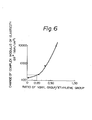
- Fig. 6 shows the relationship between the complex modulus of elasticity of a silicone gel and the ratio of vinyl groups to ethylene groups.
- In an embodiment of the present invention, a silicone resin in the form of gel is used as an addition reaction type material for sealing a semiconductor element. Figure I shows a general structure of a hydrid IC to which the present invention is applied. In the figure, reference number I denotes a flip-chip IC on a main surface of which
soldering bumps 3 are formed, andreference numeral 2 denotes a thick layer circuit board on which apredetermined conductor pattern 2A is formed, the flip-chip IC I being soldered to a given portion of theconductor pattern 2A.Reference numeral 4 denotes a silicone gel as a sealing material, 5 a case made of a resin or metal, 6 an addition reaction type silicone adhesive, 7 a cap made of a resin or metal, 8 a space of air or resin, and 9 a gap between the flip-chip IC I and thecircuit board 2 wherein thesilicone gel 4 is filled. - This strucutre of the hydrid IC generally suffers repeated temperature cycles due to surrounding temperature changes and the self generation of heat, and the strains caused by the repeated thermal stresses affect the flip-
chip IC 1. As seen in Figs. 2A, 2B, and 2C, this thermal strain comprisesshear strain 5s produced by a difference between thermal expansion coefficients of the flip-chip IC I and thecircuit board 2, as well as tensile strain δE produced by thermal expansion of thesilicone gel 4 inserted into the gap having the height of thebumps 3 between the flip-chip IC I and thecircuit board 2, to push up the flip-chip IC 1. Theshear strain 5s and the tensile strain δE increase with the increase of the chip size of the flip-chip IC I. However, the strain which causes cracking of the flip-chip IC I or breakage of thesoldering bumps 3 is the tensile strain δE. As a result, the first mode of breakage of thesoldering bumps 3 occurs due to pushing-up the flip-chip IC I by thermal expansion of thesilicone gel 4 directly below the flip-chip IC I. This is true even when the flip-chip IC I has a small chip size in a sealing structure in the prior art, as described before. - According to the present invention, the force from the
silicone gel 4 pushing up the chip I is reduced in such a way that breakage due to theshear strain 5s appears prior to breakage due to the tensile strain δE. Accordingly, enlargement of the chip I and extension of the thermal fatique life of thesoldering bumps 3 due to repeated temperature cycles can be attained, and as a result, higher and-multiplied functions can be attained in a single chip and the reliability of the whole device involving the sealing structure can be increased. - To attain a reduction of the force pushing up a chip, an investigation of the characteristics of gels was necessary, since even silicone gels having the same penetration produced different forces when pushing up a chip.
- We investigated this problem with the following formula, which is derived from a theoretical viscoelasticity analysis in which flow, deformation and the like of various elastic viscous materials are analysed.

gel 4, S the area of the flip-chip IC I, AT the width of temperature change around the flip-chip IC I, β the thermal expansion coefficient of thegel 4, H the distance between the flip-chip IC I and the thick layer printedsubstrate 2, C T a time constant of the temperature increase, and a , b, g, g, e, and B are constants. This formula shows that the pushing up force F can be calculated if G* representing the hardness of thegel 4, i.e., the complex modulus of elasticity G* concerning the Young modulus and the viscosity of thegel 4 is determined. - Accordingly, we investigated the possibility of application of the complex modulus of elasticity G*, the characteristic used in the field of reology, to the characterization of the gel. The measurement of the complex modulus of elasticity G* of a gel was carried out as shown below.
- Referring to Fig. 3A, a
gel 4 is charged between a plate II and acone 12 of a measuringunit 10 and heat cured under a standard curing condition for the gel and then cooled to 30°C. The plate II is then vibrated at an amplitude of 4° and a frequency of I Hz. As a result, the force was transmitted to atorque detector 13 through thecone 12. The mode of transmission of the force is shown in Fig. 3B. In this figure or mode, a relationship 8*(t) = G*.∈*(t) is present between the applied strain e*(t) and the resultant stress 5*(t). This G* in the just above formula is defined as the complex modulus of elasticity of thegel 4. - The relationship between the above defined complex modulus of elasticity (at 30°C and I Hz) and the pushing up force F was examined and a typical example of this relationship obtained in a specific sealing structure under a constant temperature change is shown in Fig. 4. As seen in Fig. 4, the relationship obtained in the experiment showed good coincidence with the theoretical corresponding relationship. Thus, it was shown that the pushing up force F can be expressed by the formula F = f(G*, S, ΔT, B, H, CT).
- From the above finding, the relationships between the size of an IC chip and the upper limit of the applicable complex modulus of elasticity G* (at 30°C and I Hz) of a gel were obtained, by considering the thermal surrounding conditions of a hybrid IC for a an automobile and various factors or data of an appropriate IC chip and the mounting thereof to a substrate. The relationships are shown in Fig. 5. The lines or functions X in Fig. 5 are generally expressed by the following formula.


- Although the shape of
soldering bumps 3 may be spherical, pillar-like, or otherwise, the diameter and height of the soldering bumps 3 are designed appropri ately to fit the size of a chip used. These factors should usually be designed in a limited range and thus should be considered as a constant parameter which affects the pushing up force F. IC's mounted in automobiles suffer a rigorous temperature environment in comparison with IC's for consumer appliances. The width of temperature change AT max of IC's mounted in automobiles may be as high as 200°C, considering the type of solder used (high or low melting point solder) and the Curie point at which a semiconductor loses its semiconductive characteristics. If a silicone gel is not used and air is present between the IC chip I and the printedboard 2, the maximum size of an IC chip which may be used, considering breakage thereof due to the shear strain δs, is usually assumed to be 7 to 9mm °. Thus, if the size of an IC chip is assumed to be 7 mm °, as the worst case, the upper limit of the complex modulus of elasticity G* at which the IC chip or the soldering bumps would not be broken by the pushing up force due to a gel inserted between the IC chip and the substrate, and at which the soldering bumps would be broken by the shear strain, is obtained as about 5000 dyn/cm2 from Fig. 5. On the other hand, the lower limit of the complex modulus of elasticity is obtained as about 500 dyn/cm2. Such a minimum hardness (viscosity) or complex modulus of elasticity G* is necessary for the workability of the step of sealing with a gel as well as the stability of a gel against vibration etc. suffered after potting. Thus, usually, a gel having the complex modulus of elasticity G* of about 500 to 5000 dyn/cm2, preferably 500 to 3000 dyn/cm2 considering the dispersion of various factors, can be used to attain the object of the present invention. - Next, we investigated the change of the complex modulus of elasticity G* after the lapse of time. The complex modulus of elasticity G* of a silicone gel, an addition reaction type compound, is changed or increased by reaction with another addition reaction type material such as an adhesive 6 for bonding a
cap 7 to acase 5, when the silicone gel is actually used under various envirmonmental conditions. A catalyzed addition reaction type silicone gel is made from a siloxane containing vinyl groups for forming a skeleton, a hardening agent containing hydrosilyl groups and reacting with the vinylsiloxanes to become a part of a skeleton and to form ethylene groups from the vinyl groups and the hydrosilyl groups, and a catalyst such as platinum for catalyzing the reaction between the polysiloxane and the hardening agent. Such a Pt-catalyzed addition reaction type silicone gel contains unreacted vinyl groups, which cause an increase of the cross linkage density by reaction with other ingredients to form an additional cross linkage. - Figure 6 shows the relationship between the change of the complex modulus of elasticity G* of a silicone gel and the ratio of vinyl groups (-CH=CH2) to ethylene groups (-CH2-CH2-) in the silicone gel, obtained by experiment. This silicone gel had an original complex modulus of elasticity G" of about 3000 dyn/cm' and was placed in a gas of an addition reaction type silicone adhesive which is used for assembling a hybrid IC. A similar figure or relationship between the above two could be obtained with difference adhesives, although the figure or the characteristic was shifted slightly up or down. The lower the degree the change of the complex modulus of elasticity G*, the more stable the silicone gel. According to the present invention, the change of the complex modulus of elasticity after time had lapsed, or the ratio of vinyl groups to ethylene groups, is selected such that the complex modulus of elasticity G* after increase is still lower than the upper limit of the complex modulus of elasticity G* defined previously. Here, generally speaking, from Fig. 5, it is desirable to reduce the change of the complex modulus of elasticity G* to within a range of
t 10% of the before-stated 5000 dyn/cm2, which prevents breakage of the soldering bumps or a chip due to pushing up fatigue, i.e., within several hundred dyn/cm'. Therefore, from Fig. 6, a silicone gel having a ratio of vinyl groups to ethylene groups of equal to or lower than 0.20 is very suitable, in a sealing structure according to the present invention. - As described above, according to the present invention, a sealing material for a semiconductor element has a low complex modulus of elasticity and a low content of a remaining vinyl group and so a sealed semiconductor element, particularly one used for automobiles in which the circumstance surrounding the semiconductor are severe, can have a high reliability.
- Although the present invention is described using an embodiment in which a silicone gel sealing a semiconductor element is not in contact with an addition reaction type silicone adhesive, which changes the complex modulus of elasticity of the silicone gel. The present invention can be applied to other embodiments, for example, when only an IC chip is coated with a silicone gel which is then sealed with another addition reaction type silicone material, etc.
- When a semiconductor element is an IC chip using wire bonding, or as flat package type, the IC chip will not be broken since the tension on the wire or the flame is reduced by using a silicone gel having a low complex modulus of elasticity and a low content of a remaining vinyl group.
Claims (18)
Applications Claiming Priority (2)
| Application Number | Priority Date | Filing Date | Title |
|---|---|---|---|
| JP215277/85 | 1985-09-27 | ||
| JP21527785 | 1985-09-27 |
Publications (3)
| Publication Number | Publication Date |
|---|---|
| EP0216352A2 true EP0216352A2 (en) | 1987-04-01 |
| EP0216352A3 EP0216352A3 (en) | 1989-04-26 |
| EP0216352B1 EP0216352B1 (en) | 1992-08-12 |
Family
ID=16669646
Family Applications (1)
| Application Number | Title | Priority Date | Filing Date |
|---|---|---|---|
| EP86113076A Expired - Lifetime EP0216352B1 (en) | 1985-09-27 | 1986-09-23 | Semiconductor element sealing structure |
Country Status (4)
| Country | Link |
|---|---|
| US (1) | US4812897A (en) |
| EP (1) | EP0216352B1 (en) |
| JP (1) | JPH07120733B2 (en) |
| DE (1) | DE3686383T2 (en) |
Cited By (4)
| Publication number | Priority date | Publication date | Assignee | Title |
|---|---|---|---|---|
| EP0366282A2 (en) * | 1988-10-27 | 1990-05-02 | Dow Corning S.A. | Cavity packages |
| WO1992020096A1 (en) * | 1991-05-06 | 1992-11-12 | Sensonor A.S | Arrangement for encasing a functional device, and a process for the production of same |
| GB2265497A (en) * | 1992-03-27 | 1993-09-29 | Marelli Autronica | Electronic unit, particularly for controlling functions of an internal combustion engine |
| EP0620591A1 (en) * | 1993-04-12 | 1994-10-19 | Delco Electronics Corporation | Silicone over-mould of a flip-chip device |
Families Citing this family (15)
| Publication number | Priority date | Publication date | Assignee | Title |
|---|---|---|---|---|
| US4887148A (en) * | 1988-07-15 | 1989-12-12 | Advanced Micro Devices, Inc. | Pin grid array package structure |
| US5258647A (en) * | 1989-07-03 | 1993-11-02 | General Electric Company | Electronic systems disposed in a high force environment |
| JP2927081B2 (en) * | 1991-10-30 | 1999-07-28 | 株式会社デンソー | Resin-sealed semiconductor device |
| US5323150A (en) * | 1992-06-11 | 1994-06-21 | Micron Technology, Inc. | Method for reducing conductive and convective heat loss from the battery in an RFID tag or other battery-powered devices |
| US6081028A (en) * | 1994-03-29 | 2000-06-27 | Sun Microsystems, Inc. | Thermal management enhancements for cavity packages |
| US6020219A (en) * | 1994-06-16 | 2000-02-01 | Lucent Technologies Inc. | Method of packaging fragile devices with a gel medium confined by a rim member |
| JP3353526B2 (en) * | 1995-03-23 | 2002-12-03 | 株式会社デンソー | Semiconductor package and manufacturing method thereof |
| EP0778616A3 (en) * | 1995-12-05 | 1999-03-31 | Lucent Technologies Inc. | Method of packaging devices with a gel medium confined by a rim member |
| US5767447A (en) * | 1995-12-05 | 1998-06-16 | Lucent Technologies Inc. | Electronic device package enclosed by pliant medium laterally confined by a plastic rim member |
| JP3223246B2 (en) * | 1997-07-25 | 2001-10-29 | 東レ・ダウコーニング・シリコーン株式会社 | Semiconductor device |
| JP3741855B2 (en) * | 1998-02-25 | 2006-02-01 | 信越化学工業株式会社 | Manufacturing method of semiconductor device package and organopolysiloxane composition used therefor |
| US6621173B1 (en) | 1998-07-23 | 2003-09-16 | Dow Corning Toray Silicone Co., Ltd. | Semiconductor device having an adhesive and a sealant |
| US6822868B2 (en) * | 2002-02-26 | 2004-11-23 | Delphi Technologies, Inc. | Heat sink with integrated electronics |
| US20080115772A1 (en) * | 2006-11-21 | 2008-05-22 | Ti Group Automotive Systems, L.L.C. | Fluid encapsulant for protecting electronics |
| US20120085170A1 (en) * | 2010-10-07 | 2012-04-12 | Letterneau James C | Shock Resistant Mounting for High G Shock Accelerometer |
Citations (5)
| Publication number | Priority date | Publication date | Assignee | Title |
|---|---|---|---|---|
| US3020260A (en) * | 1960-08-18 | 1962-02-06 | Dow Corning | Organosiloxane potting compound |
| US3436366A (en) * | 1965-12-17 | 1969-04-01 | Gen Electric | Silicone potting compositions comprising mixtures of organopolysiloxanes containing vinyl groups |
| US4143456A (en) * | 1976-06-28 | 1979-03-13 | Citizen Watch Commpany Ltd. | Semiconductor device insulation method |
| GB2055508A (en) * | 1979-08-01 | 1981-03-04 | Hitachi Ltd | Molded resin type semiconductor device container |
| EP0069451B1 (en) * | 1981-07-06 | 1986-09-10 | Dow Corning Corporation | Low temperature silicone gel |
Family Cites Families (8)
| Publication number | Priority date | Publication date | Assignee | Title |
|---|---|---|---|---|
| GB1397181A (en) * | 1973-01-16 | 1975-06-11 | Lucas Electrical Co Ltd | Film circuit assemblies |
| CA1081411A (en) * | 1975-12-24 | 1980-07-15 | Philipp W.H. Schuessler | Method for hermetically sealing an electronic circuit package |
| JPS5321771A (en) * | 1976-08-11 | 1978-02-28 | Sharp Kk | Electronic parts mounting structure |
| US4163072A (en) * | 1977-06-07 | 1979-07-31 | Bell Telephone Laboratories, Incorporated | Encapsulation of circuits |
| JPS5810841A (en) * | 1981-07-13 | 1983-01-21 | Mitsubishi Electric Corp | Resin sealing type semiconductor device |
| JPS59181627A (en) * | 1983-03-31 | 1984-10-16 | Toshiba Corp | Manufacture of semiconductor device |
| JPS6096456A (en) * | 1983-11-01 | 1985-05-30 | 住友ベークライト株式会社 | Non-rigid polyvinyl chloride group resin -silicon composite molded shape and manufacture thereof |
| JPS60157241A (en) * | 1984-01-26 | 1985-08-17 | Mitsubishi Electric Corp | Semiconductor device |
-
1986
- 1986-09-16 JP JP61217490A patent/JPH07120733B2/en not_active Expired - Lifetime
- 1986-09-23 DE DE8686113076T patent/DE3686383T2/en not_active Expired - Lifetime
- 1986-09-23 EP EP86113076A patent/EP0216352B1/en not_active Expired - Lifetime
-
1987
- 1987-09-01 US US07/093,159 patent/US4812897A/en not_active Expired - Lifetime
Patent Citations (5)
| Publication number | Priority date | Publication date | Assignee | Title |
|---|---|---|---|---|
| US3020260A (en) * | 1960-08-18 | 1962-02-06 | Dow Corning | Organosiloxane potting compound |
| US3436366A (en) * | 1965-12-17 | 1969-04-01 | Gen Electric | Silicone potting compositions comprising mixtures of organopolysiloxanes containing vinyl groups |
| US4143456A (en) * | 1976-06-28 | 1979-03-13 | Citizen Watch Commpany Ltd. | Semiconductor device insulation method |
| GB2055508A (en) * | 1979-08-01 | 1981-03-04 | Hitachi Ltd | Molded resin type semiconductor device container |
| EP0069451B1 (en) * | 1981-07-06 | 1986-09-10 | Dow Corning Corporation | Low temperature silicone gel |
Non-Patent Citations (2)
| Title |
|---|
| IBM TECHNICAL DISCLOSURE BULLETIN Vol. 17, Nr. 10, March 1975, page 2879, New York, US; L.S. GOLDMAN: "Getter to prevent corrosion" * |
| PATENT ABSTRACTS OF JAPAN Vol. 9, no. 159 (E-326)(1882), 4th July 1985; & JP-A-60 038 842 (HITACHI SEISAKUSHO), 28-02-1985 * |
Cited By (6)
| Publication number | Priority date | Publication date | Assignee | Title |
|---|---|---|---|---|
| EP0366282A2 (en) * | 1988-10-27 | 1990-05-02 | Dow Corning S.A. | Cavity packages |
| EP0366282A3 (en) * | 1988-10-27 | 1991-07-17 | Dow Corning S.A. | Cavity packages |
| WO1992020096A1 (en) * | 1991-05-06 | 1992-11-12 | Sensonor A.S | Arrangement for encasing a functional device, and a process for the production of same |
| GB2265497A (en) * | 1992-03-27 | 1993-09-29 | Marelli Autronica | Electronic unit, particularly for controlling functions of an internal combustion engine |
| GB2265497B (en) * | 1992-03-27 | 1995-09-20 | Marelli Autronica | Electronic unit for controlling functions of an internal combustion engine |
| EP0620591A1 (en) * | 1993-04-12 | 1994-10-19 | Delco Electronics Corporation | Silicone over-mould of a flip-chip device |
Also Published As
| Publication number | Publication date |
|---|---|
| EP0216352B1 (en) | 1992-08-12 |
| DE3686383T2 (en) | 1993-01-07 |
| DE3686383D1 (en) | 1992-09-17 |
| JPS62149157A (en) | 1987-07-03 |
| JPH07120733B2 (en) | 1995-12-20 |
| EP0216352A3 (en) | 1989-04-26 |
| US4812897A (en) | 1989-03-14 |
Similar Documents
| Publication | Publication Date | Title |
|---|---|---|
| US4812897A (en) | Semiconductor element sealing structure | |
| US5349240A (en) | Semiconductor device package having a sealing silicone gel with spherical fillers | |
| US5258650A (en) | Semiconductor device having encapsulation comprising of a thixotropic fluorosiloxane material | |
| US6104093A (en) | Thermally enhanced and mechanically balanced flip chip package and method of forming | |
| US5528456A (en) | Package with improved heat transfer structure for semiconductor device | |
| US5389739A (en) | Electronic device packaging assembly | |
| EP0189791A2 (en) | Solder interconnection structure for joining semiconductor devices to substrates, and process for making | |
| US6467139B1 (en) | Mounting structure and mounting method for surface acoustic wave element | |
| JPH09260533A (en) | Semiconductor device and its mounting structure | |
| KR0139389B1 (en) | Semiconductor device capable of preventing occurrence of a shearing | |
| US6297660B2 (en) | Test carrier with variable force applying mechanism for testing semiconductor components | |
| US6635971B2 (en) | Electronic device and optical transmission module | |
| JPH0982754A (en) | Semiconductor device | |
| CA2024338C (en) | Semiconductor strain sensor and manufacturing method thereof | |
| KR100216100B1 (en) | Flip-chip semiconductor device | |
| US5019892A (en) | Chip carrier with accumulator | |
| US6576984B2 (en) | Semiconductor apparatus and electronic system | |
| US6673858B2 (en) | Thermosetting adhesive material | |
| US7122895B2 (en) | Stud-cone bump for probe tips used in known good die carriers | |
| US5047834A (en) | High strength low stress encapsulation of interconnected semiconductor devices | |
| US6429510B1 (en) | Liquid damping of high frequency bond wire vibration | |
| JP3958927B2 (en) | Electrical equipment | |
| JPH0566024B2 (en) | ||
| JPH0340458A (en) | Semiconductor device and manufacture thereof | |
| JPH051619B2 (en) |
Legal Events
| Date | Code | Title | Description |
|---|---|---|---|
| PUAI | Public reference made under article 153(3) epc to a published international application that has entered the european phase |
Free format text: ORIGINAL CODE: 0009012 |
|
| AK | Designated contracting states |
Kind code of ref document: A2 Designated state(s): DE FR IT |
|
| PUAL | Search report despatched |
Free format text: ORIGINAL CODE: 0009013 |
|
| AK | Designated contracting states |
Kind code of ref document: A3 Designated state(s): DE FR IT |
|
| 17P | Request for examination filed |
Effective date: 19891012 |
|
| 17Q | First examination report despatched |
Effective date: 19910130 |
|
| GRAA | (expected) grant |
Free format text: ORIGINAL CODE: 0009210 |
|
| AK | Designated contracting states |
Kind code of ref document: B1 Designated state(s): DE FR IT |
|
| REF | Corresponds to: |
Ref document number: 3686383 Country of ref document: DE Date of ref document: 19920917 |
|
| ET | Fr: translation filed | ||
| ITF | It: translation for a ep patent filed |
Owner name: DR. ING. A. RACHELI & C |
|
| PLBE | No opposition filed within time limit |
Free format text: ORIGINAL CODE: 0009261 |
|
| STAA | Information on the status of an ep patent application or granted ep patent |
Free format text: STATUS: NO OPPOSITION FILED WITHIN TIME LIMIT |
|
| 26N | No opposition filed | ||
| ITPR | It: changes in ownership of a european patent |
Owner name: OFFERTA DI LICENZA AL PUBBLICO |
|
| REG | Reference to a national code |
Ref country code: FR Ref legal event code: DL |
|
| PGFP | Annual fee paid to national office [announced via postgrant information from national office to epo] |
Ref country code: FR Payment date: 20050823 Year of fee payment: 20 |
|
| PGFP | Annual fee paid to national office [announced via postgrant information from national office to epo] |
Ref country code: DE Payment date: 20050915 Year of fee payment: 20 |
|
| PGFP | Annual fee paid to national office [announced via postgrant information from national office to epo] |
Ref country code: IT Payment date: 20050927 Year of fee payment: 20 |