EP0207646A1 - Dual ion beam deposition of dense films - Google Patents
Dual ion beam deposition of dense films Download PDFInfo
- Publication number
- EP0207646A1 EP0207646A1 EP86304304A EP86304304A EP0207646A1 EP 0207646 A1 EP0207646 A1 EP 0207646A1 EP 86304304 A EP86304304 A EP 86304304A EP 86304304 A EP86304304 A EP 86304304A EP 0207646 A1 EP0207646 A1 EP 0207646A1
- Authority
- EP
- European Patent Office
- Prior art keywords
- ions
- films
- target
- substrate
- silicon
- Prior art date
- Legal status (The legal status is an assumption and is not a legal conclusion. Google has not performed a legal analysis and makes no representation as to the accuracy of the status listed.)
- Ceased
Links
Images

Classifications
-
- H—ELECTRICITY
- H01—ELECTRIC ELEMENTS
- H01L—SEMICONDUCTOR DEVICES NOT COVERED BY CLASS H10
- H01L21/00—Processes or apparatus adapted for the manufacture or treatment of semiconductor or solid state devices or of parts thereof
- H01L21/02—Manufacture or treatment of semiconductor devices or of parts thereof
- H01L21/02104—Forming layers
- H01L21/02107—Forming insulating materials on a substrate
- H01L21/02109—Forming insulating materials on a substrate characterised by the type of layer, e.g. type of material, porous/non-porous, pre-cursors, mixtures or laminates
- H01L21/02112—Forming insulating materials on a substrate characterised by the type of layer, e.g. type of material, porous/non-porous, pre-cursors, mixtures or laminates characterised by the material of the layer
- H01L21/02123—Forming insulating materials on a substrate characterised by the type of layer, e.g. type of material, porous/non-porous, pre-cursors, mixtures or laminates characterised by the material of the layer the material containing silicon
- H01L21/02164—Forming insulating materials on a substrate characterised by the type of layer, e.g. type of material, porous/non-porous, pre-cursors, mixtures or laminates characterised by the material of the layer the material containing silicon the material being a silicon oxide, e.g. SiO2
-
- C—CHEMISTRY; METALLURGY
- C03—GLASS; MINERAL OR SLAG WOOL
- C03C—CHEMICAL COMPOSITION OF GLASSES, GLAZES OR VITREOUS ENAMELS; SURFACE TREATMENT OF GLASS; SURFACE TREATMENT OF FIBRES OR FILAMENTS MADE FROM GLASS, MINERALS OR SLAGS; JOINING GLASS TO GLASS OR OTHER MATERIALS
- C03C17/00—Surface treatment of glass, not in the form of fibres or filaments, by coating
- C03C17/22—Surface treatment of glass, not in the form of fibres or filaments, by coating with other inorganic material
- C03C17/225—Nitrides
-
- C—CHEMISTRY; METALLURGY
- C03—GLASS; MINERAL OR SLAG WOOL
- C03C—CHEMICAL COMPOSITION OF GLASSES, GLAZES OR VITREOUS ENAMELS; SURFACE TREATMENT OF GLASS; SURFACE TREATMENT OF FIBRES OR FILAMENTS MADE FROM GLASS, MINERALS OR SLAGS; JOINING GLASS TO GLASS OR OTHER MATERIALS
- C03C17/00—Surface treatment of glass, not in the form of fibres or filaments, by coating
- C03C17/22—Surface treatment of glass, not in the form of fibres or filaments, by coating with other inorganic material
- C03C17/23—Oxides
- C03C17/245—Oxides by deposition from the vapour phase
-
- C—CHEMISTRY; METALLURGY
- C23—COATING METALLIC MATERIAL; COATING MATERIAL WITH METALLIC MATERIAL; CHEMICAL SURFACE TREATMENT; DIFFUSION TREATMENT OF METALLIC MATERIAL; COATING BY VACUUM EVAPORATION, BY SPUTTERING, BY ION IMPLANTATION OR BY CHEMICAL VAPOUR DEPOSITION, IN GENERAL; INHIBITING CORROSION OF METALLIC MATERIAL OR INCRUSTATION IN GENERAL
- C23C—COATING METALLIC MATERIAL; COATING MATERIAL WITH METALLIC MATERIAL; SURFACE TREATMENT OF METALLIC MATERIAL BY DIFFUSION INTO THE SURFACE, BY CHEMICAL CONVERSION OR SUBSTITUTION; COATING BY VACUUM EVAPORATION, BY SPUTTERING, BY ION IMPLANTATION OR BY CHEMICAL VAPOUR DEPOSITION, IN GENERAL
- C23C14/00—Coating by vacuum evaporation, by sputtering or by ion implantation of the coating forming material
- C23C14/06—Coating by vacuum evaporation, by sputtering or by ion implantation of the coating forming material characterised by the coating material
-
- C—CHEMISTRY; METALLURGY
- C23—COATING METALLIC MATERIAL; COATING MATERIAL WITH METALLIC MATERIAL; CHEMICAL SURFACE TREATMENT; DIFFUSION TREATMENT OF METALLIC MATERIAL; COATING BY VACUUM EVAPORATION, BY SPUTTERING, BY ION IMPLANTATION OR BY CHEMICAL VAPOUR DEPOSITION, IN GENERAL; INHIBITING CORROSION OF METALLIC MATERIAL OR INCRUSTATION IN GENERAL
- C23C—COATING METALLIC MATERIAL; COATING MATERIAL WITH METALLIC MATERIAL; SURFACE TREATMENT OF METALLIC MATERIAL BY DIFFUSION INTO THE SURFACE, BY CHEMICAL CONVERSION OR SUBSTITUTION; COATING BY VACUUM EVAPORATION, BY SPUTTERING, BY ION IMPLANTATION OR BY CHEMICAL VAPOUR DEPOSITION, IN GENERAL
- C23C14/00—Coating by vacuum evaporation, by sputtering or by ion implantation of the coating forming material
- C23C14/22—Coating by vacuum evaporation, by sputtering or by ion implantation of the coating forming material characterised by the process of coating
- C23C14/34—Sputtering
- C23C14/46—Sputtering by ion beam produced by an external ion source
-
- H—ELECTRICITY
- H01—ELECTRIC ELEMENTS
- H01L—SEMICONDUCTOR DEVICES NOT COVERED BY CLASS H10
- H01L21/00—Processes or apparatus adapted for the manufacture or treatment of semiconductor or solid state devices or of parts thereof
- H01L21/02—Manufacture or treatment of semiconductor devices or of parts thereof
- H01L21/02104—Forming layers
- H01L21/02107—Forming insulating materials on a substrate
- H01L21/02225—Forming insulating materials on a substrate characterised by the process for the formation of the insulating layer
- H01L21/0226—Forming insulating materials on a substrate characterised by the process for the formation of the insulating layer formation by a deposition process
- H01L21/02263—Forming insulating materials on a substrate characterised by the process for the formation of the insulating layer formation by a deposition process deposition from the gas or vapour phase
- H01L21/02266—Forming insulating materials on a substrate characterised by the process for the formation of the insulating layer formation by a deposition process deposition from the gas or vapour phase deposition by physical ablation of a target, e.g. sputtering, reactive sputtering, physical vapour deposition or pulsed laser deposition
-
- H—ELECTRICITY
- H01—ELECTRIC ELEMENTS
- H01L—SEMICONDUCTOR DEVICES NOT COVERED BY CLASS H10
- H01L21/00—Processes or apparatus adapted for the manufacture or treatment of semiconductor or solid state devices or of parts thereof
- H01L21/02—Manufacture or treatment of semiconductor devices or of parts thereof
- H01L21/02104—Forming layers
- H01L21/02365—Forming inorganic semiconducting materials on a substrate
- H01L21/02367—Substrates
- H01L21/0237—Materials
-
- H—ELECTRICITY
- H01—ELECTRIC ELEMENTS
- H01L—SEMICONDUCTOR DEVICES NOT COVERED BY CLASS H10
- H01L21/00—Processes or apparatus adapted for the manufacture or treatment of semiconductor or solid state devices or of parts thereof
- H01L21/02—Manufacture or treatment of semiconductor devices or of parts thereof
- H01L21/02104—Forming layers
- H01L21/02365—Forming inorganic semiconducting materials on a substrate
- H01L21/02436—Intermediate layers between substrates and deposited layers
- H01L21/02439—Materials
- H01L21/02488—Insulating materials
-
- H—ELECTRICITY
- H01—ELECTRIC ELEMENTS
- H01L—SEMICONDUCTOR DEVICES NOT COVERED BY CLASS H10
- H01L21/00—Processes or apparatus adapted for the manufacture or treatment of semiconductor or solid state devices or of parts thereof
- H01L21/02—Manufacture or treatment of semiconductor devices or of parts thereof
- H01L21/02104—Forming layers
- H01L21/02365—Forming inorganic semiconducting materials on a substrate
- H01L21/02518—Deposited layers
- H01L21/02521—Materials
- H01L21/02524—Group 14 semiconducting materials
- H01L21/02532—Silicon, silicon germanium, germanium
-
- H—ELECTRICITY
- H01—ELECTRIC ELEMENTS
- H01L—SEMICONDUCTOR DEVICES NOT COVERED BY CLASS H10
- H01L21/00—Processes or apparatus adapted for the manufacture or treatment of semiconductor or solid state devices or of parts thereof
- H01L21/02—Manufacture or treatment of semiconductor devices or of parts thereof
- H01L21/02104—Forming layers
- H01L21/02365—Forming inorganic semiconducting materials on a substrate
- H01L21/02612—Formation types
- H01L21/02617—Deposition types
- H01L21/02631—Physical deposition at reduced pressure, e.g. MBE, sputtering, evaporation
-
- H—ELECTRICITY
- H01—ELECTRIC ELEMENTS
- H01L—SEMICONDUCTOR DEVICES NOT COVERED BY CLASS H10
- H01L21/00—Processes or apparatus adapted for the manufacture or treatment of semiconductor or solid state devices or of parts thereof
- H01L21/02—Manufacture or treatment of semiconductor devices or of parts thereof
- H01L21/04—Manufacture or treatment of semiconductor devices or of parts thereof the devices having at least one potential-jump barrier or surface barrier, e.g. PN junction, depletion layer or carrier concentration layer
- H01L21/18—Manufacture or treatment of semiconductor devices or of parts thereof the devices having at least one potential-jump barrier or surface barrier, e.g. PN junction, depletion layer or carrier concentration layer the devices having semiconductor bodies comprising elements of Group IV of the Periodic System or AIIIBV compounds with or without impurities, e.g. doping materials
- H01L21/30—Treatment of semiconductor bodies using processes or apparatus not provided for in groups H01L21/20 - H01L21/26
- H01L21/31—Treatment of semiconductor bodies using processes or apparatus not provided for in groups H01L21/20 - H01L21/26 to form insulating layers thereon, e.g. for masking or by using photolithographic techniques; After treatment of these layers; Selection of materials for these layers
- H01L21/314—Inorganic layers
- H01L21/316—Inorganic layers composed of oxides or glassy oxides or oxide based glass
- H01L21/31604—Deposition from a gas or vapour
- H01L21/31608—Deposition of SiO2
- H01L21/31612—Deposition of SiO2 on a silicon body
-
- C—CHEMISTRY; METALLURGY
- C03—GLASS; MINERAL OR SLAG WOOL
- C03C—CHEMICAL COMPOSITION OF GLASSES, GLAZES OR VITREOUS ENAMELS; SURFACE TREATMENT OF GLASS; SURFACE TREATMENT OF FIBRES OR FILAMENTS MADE FROM GLASS, MINERALS OR SLAGS; JOINING GLASS TO GLASS OR OTHER MATERIALS
- C03C2217/00—Coatings on glass
- C03C2217/20—Materials for coating a single layer on glass
- C03C2217/21—Oxides
- C03C2217/229—Non-specific enumeration
-
- C—CHEMISTRY; METALLURGY
- C03—GLASS; MINERAL OR SLAG WOOL
- C03C—CHEMICAL COMPOSITION OF GLASSES, GLAZES OR VITREOUS ENAMELS; SURFACE TREATMENT OF GLASS; SURFACE TREATMENT OF FIBRES OR FILAMENTS MADE FROM GLASS, MINERALS OR SLAGS; JOINING GLASS TO GLASS OR OTHER MATERIALS
- C03C2217/00—Coatings on glass
- C03C2217/20—Materials for coating a single layer on glass
- C03C2217/21—Oxides
- C03C2217/23—Mixtures
-
- C—CHEMISTRY; METALLURGY
- C03—GLASS; MINERAL OR SLAG WOOL
- C03C—CHEMICAL COMPOSITION OF GLASSES, GLAZES OR VITREOUS ENAMELS; SURFACE TREATMENT OF GLASS; SURFACE TREATMENT OF FIBRES OR FILAMENTS MADE FROM GLASS, MINERALS OR SLAGS; JOINING GLASS TO GLASS OR OTHER MATERIALS
- C03C2217/00—Coatings on glass
- C03C2217/20—Materials for coating a single layer on glass
- C03C2217/28—Other inorganic materials
- C03C2217/281—Nitrides
-
- C—CHEMISTRY; METALLURGY
- C03—GLASS; MINERAL OR SLAG WOOL
- C03C—CHEMICAL COMPOSITION OF GLASSES, GLAZES OR VITREOUS ENAMELS; SURFACE TREATMENT OF GLASS; SURFACE TREATMENT OF FIBRES OR FILAMENTS MADE FROM GLASS, MINERALS OR SLAGS; JOINING GLASS TO GLASS OR OTHER MATERIALS
- C03C2217/00—Coatings on glass
- C03C2217/20—Materials for coating a single layer on glass
- C03C2217/28—Other inorganic materials
- C03C2217/282—Carbides, silicides
-
- C—CHEMISTRY; METALLURGY
- C03—GLASS; MINERAL OR SLAG WOOL
- C03C—CHEMICAL COMPOSITION OF GLASSES, GLAZES OR VITREOUS ENAMELS; SURFACE TREATMENT OF GLASS; SURFACE TREATMENT OF FIBRES OR FILAMENTS MADE FROM GLASS, MINERALS OR SLAGS; JOINING GLASS TO GLASS OR OTHER MATERIALS
- C03C2218/00—Methods for coating glass
- C03C2218/10—Deposition methods
- C03C2218/15—Deposition methods from the vapour phase
- C03C2218/154—Deposition methods from the vapour phase by sputtering
Definitions
- Amorphous films of acceptable density for such applications are usually achieved only by high temperature post-deposition treatments. The temperatures necessary to improve film density can have a detrimental effect on the substrate, particularly if the substrate is an integrated circuit. Accordingly, there is a need for a low temperature technique for depositing dense amorphous films.
- a novel dual ion beam process produces thin films, for example, amorphous hydrogenated silicon, silicon oxides, nitrides and other compounds, having densities very near the bulk values of the deposited materials, on substrates maintained at temperatures between 20C and 400C.
- a beam of relatively heavy sputtering ions such as argon ions, is directed at a target.
- a second beam of ions of relatively low energy is also directed at the target.
- These low energy ions may be hydrogen, oxygen, nitrogen or other ions and typically have energies less than about 20 electron volts, but not less than about 4 electron volts.
- the low energy ions combine with the target atoms or atoms sputtered from the target to form the deposition species either as atoms or molecules that are collected on a substrate.
- the deposition species impact the substrate with relatively low energy depositing a much denser film than otherwise observed in deposition by sputtering.
- the low arrival energy of the deposition species reduces structural disorder or defect formation in the deposited film producing the higher density.
- the resulting thin films show densities and dielectric constants at or very near the values usually measured only for bulk samples of the deposited materials.
- Hydrogenated amorphous silicon films deposited according to the process show increases in photoconductivity by about an order of magnitude or more over the best similar films deposited by previously known dual ion beam techniques.
- FIG. 1 An arrangement of apparatus for carrying out the novel process is shown in Figure 1.
- a beam 5 of relatively heavy sputtering ions is directed at target 1 from a conventional ion gun, not shown.
- the ion gun may be of the Kaufman type in which ions are formed in crossed electrical and magnetic fields. Electrons emitted from a central cathode follow spiral paths through the magnetic field toward a circumferential anode. The electrons form ions of gaseous atoms introduced into the gun between cathode and anode. The ions formed are accelerated out of the gun by an electrically charged accelerating grid.
- the sputtering ions are argon ions supplied to the beam source as argon gas.
- Other noble gases can be used as ion sources as well.
- the voltage applied to the ions in the sputtering beam source ranges from 750 to 1500 volts.
- a second beam 7 of low energy ions is directed at target 1 from a different direction.
- the low energy ions have energies not greater than about 20 electron volts and no less than about 3 to 4 electron volts.
- a conventional Kaufman ion source cannot produce such low energy ions while sustaining a desired beam current. Therefore, I have found it necessary to modifiy a 2.5 cm. Kaufman source to produce ions with the desired energy at an acceptable beam current.
- the screen grid is removed. As a result, the width of the dark space in the plasma within the Kaufman gun determines the beam current.
- the width of the dark space varies in a complex way with the absolute value of the anode voltage, permitting the beam current to be maintained at a desired level, although the voltage on the anode is reduced to produce ion energies between 3 and 20 electron volts.
- the ions in the second beam are also derived from a gas which may be elemental, such as hydrogen, oxygen or nitrogen, or a compound, such as silane and germane.
- substrate 1 may be heated, for example, by an electrical current flowing through a substrate holder or by heat lamps to aid the deposition process.
- the range of substrate temperatures used in the novel process are 20C to 400C.
- the substrate may, for example, be glass, quartz, silicon, a metal or metal alloy.
- the vacuum in which the process is performed is maintained at about 0.13 to 1.33 x 10 ⁇ 3 pascal.
- the target may be silicon, germanium, molybdenum, nickel, etc.
- the ions in the low energy beam may be hydrogen, oxygen, nitrogen, fluorine, etc.
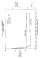
- Films of hydrogenated amorphous silicon prepared according to the novel process are shown in Figure 2 for the plotted data points corresponding to hydrogen beam voltages less than about 40 volts.
- the value of the logarithm of measured dark conductivity, the broken line, is keyed to the right ordinate and the value of the logarithm of measured photoconductivity, the solid line, is keyed to the left ordinate).
- both dark current and photoconductivity increase dramatically, more than an order of magnitude, when the hydrogen beam voltage drops below about 20 volts, i.e. when the energy of the ions is below 20 electron volts.
- a hydrogenated silicon-germanium alloy film may be deposited by using a silicon target and a low energy beam of ions formed from germane gas.
- the precise mechanism resulting in the deposition of the high density amorphous films is not known.
- a growing film is constantly bombarded with sputtered atoms or electrons of relatively high energy. These atoms may well cause some sputtering or structural damage the depositing film, such as the creation of voids, reducing its density.
- some of the sputtering gas atoms may be incorporated in the depositing film.
- the low energy ions interact with the target and/or with atoms sputtered from the target to form the depositing species.
- the substrate is not bombarded with species having energies that may damage the film.
Abstract
A novel dual ion beam sputtering process for depositing thin films of high density is described. One of the ion beams contains relatively heavy sputtering ions, such as argon ions, for ejecting atoms from a target. The second ion beam is also directed at the target and contains ions having energies of at least 3 electron volts and less than about 20 electron volts. The products of the beams are collected on a substrate as a thin film. High density, hydrogenated amorphous semiconductor films, oxide and nitride films, and other films, may be deposited according to the process. The films have densities nearly equal those observed for bulk samples of the same materials. Hydrogenated amorphous silicon films deposited by the process exhibit enhanced photoconductivity.
Description
- The technique of thin film deposition by ion beam sputtering is well established. In the typical process an ion beam of relatively heavy ions is directed at a target to cause ejection of atomic particles. These particles are collected on a substrate to form a film. In some variations of the technique, two ion beam sources are used; usually a sputtering beam is directed at a target and the second beam is directed at the depositing film. For a general description of these techniques see Weissmantel, et al., Preparation of Hard Coatings by Ion Beam Methods, 63 Thin Film Solids, 315-325 (1979). In some methods, two relatively high energy ion beams, one containing noble gas ions and the other containing different types of ions, are directed at a target. The sputtered products are then collected on a substrate. See German Democratic Republic patent 149,549.
- An improved technique for dual beam deposition of thin films has recently been devised. In this technique, an ion beam composed of sputtering ions is directed at a target and a second ion beam composed of hydrogen or halogen ions is also directed at the target, rather than at the depositing film. When the target is silicon and the second beam is hydrogen ions, improved hydrogenated amorphous silicon films are prepared. See European patent application 0177115 published April 9, 1986.
- While the referenced techniques can provide electronic quality semiconductor films, it is also desirable to deposit high density films for use as diffusion masks in integrated circuit manufacture and for use as corrosion and wear resistant coatings on metals. Amorphous films of acceptable density for such applications are usually achieved only by high temperature post-deposition treatments. The temperatures necessary to improve film density can have a detrimental effect on the substrate, particularly if the substrate is an integrated circuit. Accordingly, there is a need for a low temperature technique for depositing dense amorphous films.
- In the invention a novel dual ion beam process produces thin films, for example, amorphous hydrogenated silicon, silicon oxides, nitrides and other compounds, having densities very near the bulk values of the deposited materials, on substrates maintained at temperatures between 20C and 400C. In the novel process a beam of relatively heavy sputtering ions, such as argon ions, is directed at a target. A second beam of ions of relatively low energy is also directed at the target. These low energy ions, may be hydrogen, oxygen, nitrogen or other ions and typically have energies less than about 20 electron volts, but not less than about 4 electron volts.
- The low energy ions combine with the target atoms or atoms sputtered from the target to form the deposition species either as atoms or molecules that are collected on a substrate. The deposition species impact the substrate with relatively low energy depositing a much denser film than otherwise observed in deposition by sputtering.
- In contrast to known dual ion beam processes, in the new process, the low arrival energy of the deposition species reduces structural disorder or defect formation in the deposited film producing the higher density.
- The resulting thin films show densities and dielectric constants at or very near the values usually measured only for bulk samples of the deposited materials. Hydrogenated amorphous silicon films deposited according to the process show increases in photoconductivity by about an order of magnitude or more over the best similar films deposited by previously known dual ion beam techniques.
- Figure 1 is a schematic view of the arrangement of a target, substrate and ion beam directions for performing the inventive process.
- Figure 2 is a graph of measured photoconductivity and dark current of hydrogenated amorphous silicon films deposited by a known dual ion beam process and according to the invention.
- Figure 3 is a graph of the measured hydrogen incorporation in hydrogenated amorphous silicon films deposited by a known dual ion beam process and according to the invention.
- An arrangement of apparatus for carrying out the novel process is shown in Figure 1. A
sputter target 1, which is gradually consumed in the sputtering process, is disposed opposite a substrate 3, on which the deposition species produced in the process are collected to form film. Abeam 5 of relatively heavy sputtering ions is directed attarget 1 from a conventional ion gun, not shown. The ion gun may be of the Kaufman type in which ions are formed in crossed electrical and magnetic fields. Electrons emitted from a central cathode follow spiral paths through the magnetic field toward a circumferential anode. The electrons form ions of gaseous atoms introduced into the gun between cathode and anode. The ions formed are accelerated out of the gun by an electrically charged accelerating grid. Just inside the gun from the accelerating grid is a screen grid maintained at a slightly different potential than the accelerating grid to protect the accelerating grid from ion impacts. Typically the sputtering ions are argon ions supplied to the beam source as argon gas. Other noble gases can be used as ion sources as well. The voltage applied to the ions in the sputtering beam source ranges from 750 to 1500 volts. - A
second beam 7 of low energy ions is directed attarget 1 from a different direction. To achieve the best results, I prefer that the low energy ions have energies not greater than about 20 electron volts and no less than about 3 to 4 electron volts. A conventional Kaufman ion source cannot produce such low energy ions while sustaining a desired beam current. Therefore, I have found it necessary to modifiy a 2.5 cm. Kaufman source to produce ions with the desired energy at an acceptable beam current. In order to increase the current of the beam at low voltage, the screen grid is removed. As a result, the width of the dark space in the plasma within the Kaufman gun determines the beam current. The width of the dark space varies in a complex way with the absolute value of the anode voltage, permitting the beam current to be maintained at a desired level, although the voltage on the anode is reduced to produce ion energies between 3 and 20 electron volts. The ions in the second beam are also derived from a gas which may be elemental, such as hydrogen, oxygen or nitrogen, or a compound, such as silane and germane. - In the arrangement of Figure 1,
substrate 1 may be heated, for example, by an electrical current flowing through a substrate holder or by heat lamps to aid the deposition process. Typically, the range of substrate temperatures used in the novel process are 20C to 400C. The substrate may, for example, be glass, quartz, silicon, a metal or metal alloy. Typically, the vacuum in which the process is performed is maintained at about 0.13 to 1.33 x 10⁻³ pascal. - In the arrangement of Fig. 1, the target may be silicon, germanium, molybdenum, nickel, etc. The ions in the low energy beam may be hydrogen, oxygen, nitrogen, fluorine, etc. By choosing the proper combinations from these exemplary lists, films of silicon oxides, hydrogenated silicon, nitrides, germanium-silicon alloys and other compounds and alloys can be produced.
- I have deposited numerous films of silicon oxides at room temperature by the novel process using argon ions as a sputtering beam, a silicon target and a low energy oxygen ion beam. Those oxide films have been analyzed by spectroscopic ellipsometry and show the same dielectric constant as does bulk silicon dioxide, even when the films are very thin. The same technique was used to measure the density of the films and demonstrated that the films had already reached their maximum density when only 2 nanometers thick. Using x-ray spectroscopy techniques, it was determined that the film had a formula of SiOx where x equalled 2.0.
- Many hydrogenated amorphous silicon films have been deposited by the new process using an argon beam, a silicon target and low energy hydrogen beam. These films not only have higher densities than other dual ion beam sputtered hydrogenated silicon films, but show substantially improved photoconductives. In Figure 2, the measured dark conductivity (broken line) and photoconductivity (solid line) are plotted for films deposited according to the new process and by a known dual ion beam process in which both beams are directed at the source. The latter process is disclosed in European patent application 0177115 published April 9, 1986. In that application, the hydrogen beam voltage employed was 100, 150 or 200 volts and the deposited films showed an optimized quality at a beam voltage of 150 volts. Those films showed maximum logarithmic dark conductivities and photoconductivities of -11 and -6.8 respectively. Films prepared according to that earlier disclosed process are shown in Figure 2 for hydrogen ion beam voltages of about 100 volts or more. Hydrogen beam voltage is plotted on the abscissa.
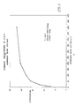
- Films of hydrogenated amorphous silicon prepared according to the novel process are shown in Figure 2 for the plotted data points corresponding to hydrogen beam voltages less than about 40 volts. (The value of the logarithm of measured dark conductivity, the broken line, is keyed to the right ordinate and the value of the logarithm of measured photoconductivity, the solid line, is keyed to the left ordinate). As is apparent from the graph, both dark current and photoconductivity increase dramatically, more than an order of magnitude, when the hydrogen beam voltage drops below about 20 volts, i.e. when the energy of the ions is below 20 electron volts. The results plotted in Figure 2 were measured from films deposited on substrates at temperatures of 150C, with a sputtering beam of argon ions at 1000 volts and 30 milliampere current and a hydrogen beam current of 10 milliamperes. The amount of hydrogen incorporated in the films decreases sharply as the hydrogen beam voltage is reduced to the range of the novel process. See Figure 3.
- In order to optimize the improved results shown in Figure 2, I find it important to avoid contamination of the depositing films by heavy metal ions. While the arrangement of Figure 1 shows the sputtering and low energy ion beams striking only the target, in practice some of the ions in the beams miss the target and can strike the walls of the vacuum chamber in which the deposition takes place. Since the typical vacuum chamber may have a metal wall or base plate, the stray ions can sputter heavy metal ions into the chamber and onto the substrate. To avoid this source of contamination, I prefer to use a curtain of high purity silicon wafers to shroud the volume between the target and substrate.
- A hydrogenated silicon-germanium alloy film may be deposited by using a silicon target and a low energy beam of ions formed from germane gas.
- The precise mechanism resulting in the deposition of the high density amorphous films is not known. In the typical sputtering process a growing film is constantly bombarded with sputtered atoms or electrons of relatively high energy. These atoms may well cause some sputtering or structural damage the depositing film, such as the creation of voids, reducing its density. In addition, some of the sputtering gas atoms may be incorporated in the depositing film. In the novel process the low energy ions interact with the target and/or with atoms sputtered from the target to form the depositing species. The substrate is not bombarded with species having energies that may damage the film. In addition, the number of sputtering gas ions incorporated into films prepared according to the novel process is quite low. A typical secondary ion mass spectroscopy (SIMS) measurement of films deposited according to the invention shows about 10⁻³ percent of argon in a hydrogenated amorphous silicon film.
Claims (9)
1. A process for depositing a film on a substrate, said film being composed of at least first and second elements, said process comprising simultaneously directing a first beam of ions effective in sputtering and a second beam of ions including ions of said second element against a target including said first element, and collecting on said substrate the products of said beams, characterized in that said ions of said second element have energies not exceeding 20 electron volts.
2. The process of claim 1 characterized in that said ions of said second element have energies not less than 3 electron volts.
3. The process of claim 1 wherein said first element is selected from the group consisting essentially of silicon, germanium, molydenum, nickel and mixtures thereof.
4. The process of claim 1 wherein said second element is selected from the group consisting essentially of hydrogen, oxygen, nitrogen, fluorine, germanium, silicon and mixtures thereof.
5. The process of claim 1 wherein said ions effective in sputtering comprise argon ions.
6. The process of claim 1 wherein said first element consists of silicon and said second element consists of germanium.
7. The process of claim 1 including maintaining said substrate at a temperature of between 20C to 400C during said deposition process.
8. The process of claim 1 wherein said substrate is selected from the group consisting essentially of glass, quartz, silicon, metallic elements and metal alloys.
9. The process of claim 1 including maintaining the ambient pressure during said deposition process between 0.13 to 1.3 x 10⁻³ pascal.
Applications Claiming Priority (2)
| Application Number | Priority Date | Filing Date | Title |
|---|---|---|---|
| US749833 | 1985-06-28 | ||
| US06/749,833 US4673475A (en) | 1985-06-28 | 1985-06-28 | Dual ion beam deposition of dense films |
Publications (1)
| Publication Number | Publication Date |
|---|---|
| EP0207646A1 true EP0207646A1 (en) | 1987-01-07 |
Family
ID=25015402
Family Applications (1)
| Application Number | Title | Priority Date | Filing Date |
|---|---|---|---|
| EP86304304A Ceased EP0207646A1 (en) | 1985-06-28 | 1986-06-05 | Dual ion beam deposition of dense films |
Country Status (4)
| Country | Link |
|---|---|
| US (1) | US4673475A (en) |
| EP (1) | EP0207646A1 (en) |
| JP (1) | JPS624313A (en) |
| IL (1) | IL78921A (en) |
Cited By (10)
| Publication number | Priority date | Publication date | Assignee | Title |
|---|---|---|---|---|
| WO1994023477A1 (en) * | 1993-03-26 | 1994-10-13 | Honeywell Inc. | Method of fabricating diode lasers using ion beam deposition |
| EP0529822B1 (en) * | 1991-08-16 | 2000-05-03 | Visx Incorporated | Apparatus for combined cylindrical and spherical eye corrections |
| US7713632B2 (en) | 2004-07-12 | 2010-05-11 | Cardinal Cg Company | Low-maintenance coatings |
| US7923114B2 (en) | 2004-12-03 | 2011-04-12 | Cardinal Cg Company | Hydrophilic coatings, methods for depositing hydrophilic coatings, and improved deposition technology for thin films |
| US7989094B2 (en) | 2006-04-19 | 2011-08-02 | Cardinal Cg Company | Opposed functional coatings having comparable single surface reflectances |
| US8092660B2 (en) | 2004-12-03 | 2012-01-10 | Cardinal Cg Company | Methods and equipment for depositing hydrophilic coatings, and deposition technologies for thin films |
| WO2012050597A1 (en) * | 2010-10-15 | 2012-04-19 | Guardian Industries Corp. | Method of treating the surface of a soda lime silica glass substrate, surface-treated glass substrate, and device incorporating the same |
| US8506768B2 (en) | 2007-09-14 | 2013-08-13 | Cardinal Cg Company | Low-maintenance coatings, and methods for producing low-maintenance coatings |
| US9738967B2 (en) | 2006-07-12 | 2017-08-22 | Cardinal Cg Company | Sputtering apparatus including target mounting and control |
| US10604442B2 (en) | 2016-11-17 | 2020-03-31 | Cardinal Cg Company | Static-dissipative coating technology |
Families Citing this family (18)
| Publication number | Priority date | Publication date | Assignee | Title |
|---|---|---|---|---|
| US5514885A (en) * | 1986-10-09 | 1996-05-07 | Myrick; James J. | SOI methods and apparatus |
| US4776925A (en) * | 1987-04-30 | 1988-10-11 | The Trustees Of Columbia University In The City Of New York | Method of forming dielectric thin films on silicon by low energy ion beam bombardment |
| JP2713481B2 (en) * | 1989-12-04 | 1998-02-16 | 株式会社日立製作所 | Method and apparatus for forming multi-layer thin film by ion beam sputtering |
| US5246885A (en) * | 1989-12-13 | 1993-09-21 | International Business Machines Corporation | Deposition method for high aspect ratio features using photoablation |
| JPH03202461A (en) * | 1989-12-29 | 1991-09-04 | Nissin Electric Co Ltd | Formation of highly insulating thin silicon oxide film |
| US5601654A (en) * | 1996-05-31 | 1997-02-11 | The Regents Of The University Of California, Office Of Technology Transfer | Flow-through ion beam source |
| GB2321063A (en) * | 1997-01-08 | 1998-07-15 | Oxford Plasma Technology Ltd | Reactive particle beam sputtering |
| US6461982B2 (en) * | 1997-02-27 | 2002-10-08 | Micron Technology, Inc. | Methods for forming a dielectric film |
| US6728429B1 (en) | 2000-02-16 | 2004-04-27 | Biotell, Inc. | Optical detection |
| GB0127251D0 (en) * | 2001-11-13 | 2002-01-02 | Nordiko Ltd | Apparatus |
| US20050118533A1 (en) * | 2002-03-01 | 2005-06-02 | Mirkarimi Paul B. | Planarization of substrate pits and scratches |
| CN100355089C (en) * | 2003-07-04 | 2007-12-12 | 云南大学 | Method for preparing modified infrared detecting material - amorphous SiGe film |
| EP1713736B1 (en) | 2003-12-22 | 2016-04-27 | Cardinal CG Company | Graded photocatalytic coatings and methods of making such coatings |
| KR100612868B1 (en) * | 2004-11-08 | 2006-08-14 | 삼성전자주식회사 | Fabrication method of Si film |
| JP4162094B2 (en) * | 2006-05-30 | 2008-10-08 | 三菱重工業株式会社 | Devices by room temperature bonding, device manufacturing method and room temperature bonding apparatus |
| US9347127B2 (en) * | 2012-07-16 | 2016-05-24 | Veeco Instruments, Inc. | Film deposition assisted by angular selective etch on a surface |
| RU174338U1 (en) * | 2017-01-24 | 2017-10-11 | Акционерное общество "Ритм" Тверское производство тормозной аппаратуры (АО "Ритм" ТПТА) | BALL VALVE RAILWAY RAILWAY COMPOSITION |
| CN112481586A (en) * | 2019-09-12 | 2021-03-12 | 中国科学院物理研究所 | Preparation method of superconducting combined film, product and application thereof |
Citations (10)
| Publication number | Priority date | Publication date | Assignee | Title |
|---|---|---|---|---|
| US3491015A (en) * | 1967-04-04 | 1970-01-20 | Automatic Fire Control Inc | Method of depositing elemental material from a low pressure electrical discharge |
| US3915765A (en) * | 1973-06-25 | 1975-10-28 | Bell Telephone Labor Inc | MBE technique for fabricating semiconductor devices having low series resistance |
| US3992233A (en) * | 1975-03-10 | 1976-11-16 | The Secretary Of State For Defence In Her Britannic Majesty's Government Of The United Kingdom Of Great Britain And Northern Ireland | Surface treatment of III-V compound crystals |
| US4086108A (en) * | 1976-06-24 | 1978-04-25 | Agency Of Industrial Science & Technology | Selective doping crystal growth method |
| US4147573A (en) * | 1977-04-05 | 1979-04-03 | Futaba Denshi Kogyo K. K. | Method of depositing III-V compounds on group IV element wafers by the cluster ion technique |
| US4255208A (en) * | 1979-05-25 | 1981-03-10 | Ramot University Authority For Applied Research And Industrial Development Ltd. | Method of producing monocrystalline semiconductor films utilizing an intermediate water dissolvable salt layer |
| GB1600218A (en) * | 1977-06-06 | 1981-10-14 | King W J | Ion beam intplantation |
| US4495044A (en) * | 1983-05-17 | 1985-01-22 | The United States Of America As Represented By The Administrator Of The National Aeronautics And Space Administration | Diamondlike flakes |
| US4522844A (en) * | 1983-09-30 | 1985-06-11 | The United States Of America As Represented By The Administrator, National Aeronautics And Space Administration | Corrosion resistant coating |
| EP0177115A1 (en) * | 1984-09-04 | 1986-04-09 | The Standard Oil Company | Dual ion beam deposition of amorphous semiconductor films |
Family Cites Families (2)
| Publication number | Priority date | Publication date | Assignee | Title |
|---|---|---|---|---|
| DD149549A1 (en) * | 1980-03-24 | 1981-07-15 | Hinneberg Hans Juergen | METHOD FOR PRODUCING AMORPHAL SEMICONDUCTOR LAYERS BY ION EXTRACTING |
| US4376688A (en) * | 1981-04-03 | 1983-03-15 | Xerox Corporation | Method for producing semiconductor films |
-
1985
- 1985-06-28 US US06/749,833 patent/US4673475A/en not_active Expired - Fee Related
-
1986
- 1986-05-26 IL IL78921A patent/IL78921A/en unknown
- 1986-06-05 EP EP86304304A patent/EP0207646A1/en not_active Ceased
- 1986-06-25 JP JP61149342A patent/JPS624313A/en active Pending
Patent Citations (10)
| Publication number | Priority date | Publication date | Assignee | Title |
|---|---|---|---|---|
| US3491015A (en) * | 1967-04-04 | 1970-01-20 | Automatic Fire Control Inc | Method of depositing elemental material from a low pressure electrical discharge |
| US3915765A (en) * | 1973-06-25 | 1975-10-28 | Bell Telephone Labor Inc | MBE technique for fabricating semiconductor devices having low series resistance |
| US3992233A (en) * | 1975-03-10 | 1976-11-16 | The Secretary Of State For Defence In Her Britannic Majesty's Government Of The United Kingdom Of Great Britain And Northern Ireland | Surface treatment of III-V compound crystals |
| US4086108A (en) * | 1976-06-24 | 1978-04-25 | Agency Of Industrial Science & Technology | Selective doping crystal growth method |
| US4147573A (en) * | 1977-04-05 | 1979-04-03 | Futaba Denshi Kogyo K. K. | Method of depositing III-V compounds on group IV element wafers by the cluster ion technique |
| GB1600218A (en) * | 1977-06-06 | 1981-10-14 | King W J | Ion beam intplantation |
| US4255208A (en) * | 1979-05-25 | 1981-03-10 | Ramot University Authority For Applied Research And Industrial Development Ltd. | Method of producing monocrystalline semiconductor films utilizing an intermediate water dissolvable salt layer |
| US4495044A (en) * | 1983-05-17 | 1985-01-22 | The United States Of America As Represented By The Administrator Of The National Aeronautics And Space Administration | Diamondlike flakes |
| US4522844A (en) * | 1983-09-30 | 1985-06-11 | The United States Of America As Represented By The Administrator, National Aeronautics And Space Administration | Corrosion resistant coating |
| EP0177115A1 (en) * | 1984-09-04 | 1986-04-09 | The Standard Oil Company | Dual ion beam deposition of amorphous semiconductor films |
Non-Patent Citations (3)
| Title |
|---|
| PATENT ABSTRACTS OF JAPAN, unexamined applications, C field, vol. 7, no. 122, May 26, 1983 THE PATENT OFFICE JAPANESE GOVERNMENT page 157 C 168 * JP-A 58 42 771 (SUMITOMO DENKI KOGYO K.K.) * * |
| PATENT ABSTRACTS OF JAPAN, unexamined applications, C field, vol. 9, no. 21, January 29, 1985 THE PATENT OFFICE JAPANESE GOVERNMENT page 149 C 263 * JP-A 59 170 270 (TOSHIBA K.K.) * * |
| PATENT ABSTRACTS OF JAPAN, unexamined applications, C field, vol. 9, no. 52, March 6, 1985 THE PATENT OFFICE JAPANESE GOVERNMENT page 3 C 269 * JP-A 59 190 357(HIRONOBU SATOU) * * |
Cited By (15)
| Publication number | Priority date | Publication date | Assignee | Title |
|---|---|---|---|---|
| EP0529822B1 (en) * | 1991-08-16 | 2000-05-03 | Visx Incorporated | Apparatus for combined cylindrical and spherical eye corrections |
| WO1994023477A1 (en) * | 1993-03-26 | 1994-10-13 | Honeywell Inc. | Method of fabricating diode lasers using ion beam deposition |
| US7713632B2 (en) | 2004-07-12 | 2010-05-11 | Cardinal Cg Company | Low-maintenance coatings |
| USRE43817E1 (en) | 2004-07-12 | 2012-11-20 | Cardinal Cg Company | Low-maintenance coatings |
| USRE44155E1 (en) | 2004-07-12 | 2013-04-16 | Cardinal Cg Company | Low-maintenance coatings |
| US7923114B2 (en) | 2004-12-03 | 2011-04-12 | Cardinal Cg Company | Hydrophilic coatings, methods for depositing hydrophilic coatings, and improved deposition technology for thin films |
| US8092660B2 (en) | 2004-12-03 | 2012-01-10 | Cardinal Cg Company | Methods and equipment for depositing hydrophilic coatings, and deposition technologies for thin films |
| US7989094B2 (en) | 2006-04-19 | 2011-08-02 | Cardinal Cg Company | Opposed functional coatings having comparable single surface reflectances |
| US9738967B2 (en) | 2006-07-12 | 2017-08-22 | Cardinal Cg Company | Sputtering apparatus including target mounting and control |
| US8506768B2 (en) | 2007-09-14 | 2013-08-13 | Cardinal Cg Company | Low-maintenance coatings, and methods for producing low-maintenance coatings |
| US8696879B2 (en) | 2007-09-14 | 2014-04-15 | Cardinal Cg Company | Low-maintenance coating technology |
| US8541792B2 (en) | 2010-10-15 | 2013-09-24 | Guardian Industries Corp. | Method of treating the surface of a soda lime silica glass substrate, surface-treated glass substrate, and device incorporating the same |
| WO2012050597A1 (en) * | 2010-10-15 | 2012-04-19 | Guardian Industries Corp. | Method of treating the surface of a soda lime silica glass substrate, surface-treated glass substrate, and device incorporating the same |
| US10604442B2 (en) | 2016-11-17 | 2020-03-31 | Cardinal Cg Company | Static-dissipative coating technology |
| US11325859B2 (en) | 2016-11-17 | 2022-05-10 | Cardinal Cg Company | Static-dissipative coating technology |
Also Published As
| Publication number | Publication date |
|---|---|
| JPS624313A (en) | 1987-01-10 |
| IL78921A0 (en) | 1986-09-30 |
| IL78921A (en) | 1989-12-15 |
| US4673475A (en) | 1987-06-16 |
Similar Documents
| Publication | Publication Date | Title |
|---|---|---|
| US4673475A (en) | Dual ion beam deposition of dense films | |
| Ellmer et al. | Reactive magnetron sputtering of transparent conductive oxide thin films: Role of energetic particle (ion) bombardment | |
| Waits | Planar magnetron sputtering | |
| Hoffman | Stress and property control in sputtered metal films without substrate bias | |
| US4376688A (en) | Method for producing semiconductor films | |
| US4828870A (en) | Method of forming a thin aluminum film | |
| US4132614A (en) | Etching by sputtering from an intermetallic target to form negative metallic ions which produce etching of a juxtaposed substrate | |
| JPH0381294B2 (en) | ||
| Ehrich et al. | The anodic vacuum arc and its application to coating | |
| Halverson et al. | Effects of charge neutralization on ion‐beam‐deposited boron nitride films | |
| Sundaram et al. | Deposition and X-ray photoelectron spectroscopy studies on sputtered cerium dioxide thin films | |
| Komiya et al. | Formation of thick titanium carbide films by the hollow cathode discharge reactive deposition process | |
| US7438955B2 (en) | Titanium nitride thin film formation on metal substrate by chemical vapor deposition in a magnetized sheet plasma source | |
| Taga et al. | Role of kinetic energy of sputtered particles in thin film formation | |
| McClanahan et al. | Production of thin films by controlled deposition of sputtered material | |
| Viloan et al. | Tuning the stress in TiN films by regulating the doubly charged ion fraction in a reactive HiPIMS discharge | |
| EP0269112A2 (en) | Method of forming a thin crystalline metal film | |
| US4038216A (en) | Material and method of making secondary-electron emitters | |
| Richter et al. | Fundamental mechanisms of titanium nitride formation by dc. magnetron sputtering | |
| US5989990A (en) | Tinoxide thin film, preparation thereof, and gas detecting sensor using thereof | |
| Weissmantel et al. | Ion beam techniques for thin and thick film deposition | |
| Borah et al. | Study on the influence of nitrogen on titanium nitride in a dc post magnetron sputtering plasma system | |
| Sone et al. | Sputtering of silicon carbide coatings by low-energy hydrogen ions | |
| EP0360994B1 (en) | Apparatus and method for producing diamond films at low temperatures | |
| Holland | A review of plasma process studies |
Legal Events
| Date | Code | Title | Description |
|---|---|---|---|
| PUAI | Public reference made under article 153(3) epc to a published international application that has entered the european phase |
Free format text: ORIGINAL CODE: 0009012 |
|
| AK | Designated contracting states |
Kind code of ref document: A1 Designated state(s): DE FR GB IT NL |
|
| 17P | Request for examination filed |
Effective date: 19870625 |
|
| 17Q | First examination report despatched |
Effective date: 19890629 |
|
| STAA | Information on the status of an ep patent application or granted ep patent |
Free format text: STATUS: THE APPLICATION HAS BEEN REFUSED |
|
| 18R | Application refused |
Effective date: 19900519 |
|
| RIN1 | Information on inventor provided before grant (corrected) |
Inventor name: WINDISCHMANN, HENRY |