EP0207188A2 - Resin composition for solder resist ink - Google Patents
Resin composition for solder resist ink Download PDFInfo
- Publication number
- EP0207188A2 EP0207188A2 EP85111307A EP85111307A EP0207188A2 EP 0207188 A2 EP0207188 A2 EP 0207188A2 EP 85111307 A EP85111307 A EP 85111307A EP 85111307 A EP85111307 A EP 85111307A EP 0207188 A2 EP0207188 A2 EP 0207188A2
- Authority
- EP
- European Patent Office
- Prior art keywords
- resin
- composition
- meth
- acrylates
- poly
- Prior art date
- Legal status (The legal status is an assumption and is not a legal conclusion. Google has not performed a legal analysis and makes no representation as to the accuracy of the status listed.)
- Granted
Links
Classifications
-
- G—PHYSICS
- G03—PHOTOGRAPHY; CINEMATOGRAPHY; ANALOGOUS TECHNIQUES USING WAVES OTHER THAN OPTICAL WAVES; ELECTROGRAPHY; HOLOGRAPHY
- G03F—PHOTOMECHANICAL PRODUCTION OF TEXTURED OR PATTERNED SURFACES, e.g. FOR PRINTING, FOR PROCESSING OF SEMICONDUCTOR DEVICES; MATERIALS THEREFOR; ORIGINALS THEREFOR; APPARATUS SPECIALLY ADAPTED THEREFOR
- G03F7/00—Photomechanical, e.g. photolithographic, production of textured or patterned surfaces, e.g. printing surfaces; Materials therefor, e.g. comprising photoresists; Apparatus specially adapted therefor
- G03F7/004—Photosensitive materials
- G03F7/027—Non-macromolecular photopolymerisable compounds having carbon-to-carbon double bonds, e.g. ethylenic compounds
- G03F7/032—Non-macromolecular photopolymerisable compounds having carbon-to-carbon double bonds, e.g. ethylenic compounds with binders
-
- B—PERFORMING OPERATIONS; TRANSPORTING
- B23—MACHINE TOOLS; METAL-WORKING NOT OTHERWISE PROVIDED FOR
- B23K—SOLDERING OR UNSOLDERING; WELDING; CLADDING OR PLATING BY SOLDERING OR WELDING; CUTTING BY APPLYING HEAT LOCALLY, e.g. FLAME CUTTING; WORKING BY LASER BEAM
- B23K35/00—Rods, electrodes, materials, or media, for use in soldering, welding, or cutting
- B23K35/22—Rods, electrodes, materials, or media, for use in soldering, welding, or cutting characterised by the composition or nature of the material
- B23K35/224—Anti-weld compositions; Braze stop-off compositions
-
- H—ELECTRICITY
- H05—ELECTRIC TECHNIQUES NOT OTHERWISE PROVIDED FOR
- H05K—PRINTED CIRCUITS; CASINGS OR CONSTRUCTIONAL DETAILS OF ELECTRIC APPARATUS; MANUFACTURE OF ASSEMBLAGES OF ELECTRICAL COMPONENTS
- H05K3/00—Apparatus or processes for manufacturing printed circuits
- H05K3/22—Secondary treatment of printed circuits
- H05K3/28—Applying non-metallic protective coatings
- H05K3/285—Permanent coating compositions
- H05K3/287—Photosensitive compositions
-
- H—ELECTRICITY
- H05—ELECTRIC TECHNIQUES NOT OTHERWISE PROVIDED FOR
- H05K—PRINTED CIRCUITS; CASINGS OR CONSTRUCTIONAL DETAILS OF ELECTRIC APPARATUS; MANUFACTURE OF ASSEMBLAGES OF ELECTRICAL COMPONENTS
- H05K2203/00—Indexing scheme relating to apparatus or processes for manufacturing printed circuits covered by H05K3/00
- H05K2203/07—Treatments involving liquids, e.g. plating, rinsing
- H05K2203/0779—Treatments involving liquids, e.g. plating, rinsing characterised by the specific liquids involved
- H05K2203/0783—Using solvent, e.g. for cleaning; Regulating solvent content of pastes or coatings for adjusting the viscosity
Definitions
- This invention relates to a new and useful resin composition for use in solder resist ink. More specifically, it relates to a resin composition having excellent heat resistance and dielectric resistance properties for use in printed wiring circuit boards, comprising a vinyl ester resin derived from a specific epoxy resin, a photopolymerization initiator and an amine-type curing agent.
- the present invention provides a resin composition for a liquid photographic image-type solder mask ink.
- This solder mask ink is used in place of a conventional dry film developing-type solder resist ink to form a resist pattern by coating the liquid photo resist ink on the entire surface of a printed wiring circuit board, exposing the coated film to the irradiation of active energy light through a photomask and then developing the exposed film.
- the solder resist ink is required to have dielectric resistance, heat resistance, adhesion, chemical resistance, screen printability, etc. to avoid its adhesion to unwanted parts and protect the circuit on the printed wiring circuit board in the soldering of parts to the printed circuit board.
- heat-curable solder resist inks of the melamine resin type were used. Later, heat-curable solder resist inks of the epoxy resin type having superior heat resistance, hardness, adhesion, chemical resistance, etc. were developed and have gained widespread use in printed wiring circuit boards of industrial appliances such as computers that require high reliability.
- ultraviolet- curable solder resist inks based on acrylated epoxy resins or urethane resins have gained widespread acceptance in place of the heat-curable solder resist inks of the epoxy resin type.
- the ultraviolet- curable solder resists are cured by radical reaction induced by the irradiation of ultraviolet light. When a film of the coated resist is thick, curing of its interior is slow.
- the thickness of conductors is as large as at least 70 micrometers when it is copper-plated or Sn/Pb-plated, the solder resist to be coated on it necessarily has a thickness of at least 50 micrometers in part. Accordingly, parts not irradiated with ultraviolet light, for example, the underside of the edge of the circuit, are not completely cured, and are liable to have low dielectric resistance and permit electro-migration. To prevent such troubles, therefore, it is necessary to adjust the thickness of the resist film to less than 20 micrometers by decreasing the mesh size of the screen and reducing the thickness of the emulsion film.
- the use of the ultraviolet light-curable solder resist inks has been limited to copper conductors in general household appliances on which they may be coated to a thickness of about 35 micrometers.
- the industiral printed circuit boards have also required increased precision in the pattern density of the circuit. Previously, the pattern density was two lines between IC pads, but now 3 to 5 lines between IC pads are desired.
- the ultraviolet light-curable solder resist ink used in the screen printing process contains mono- to tri-functional monomers such as 2-hydroxyethyl acrylate and trimethylolpropane triacrylate and various acrylate oligomers. These substances migrate during the screen printing, and bring about the serious defect that when such a solder resist ink is used, for example, in a printed wiring circuit board having a pattern density of at least 2 lines between IC pads, soldering cannot be well effected. To prevent this situation, it has been the practice to increase photo resolution by reducing the thickness of the coated film. By such a method, however, the solder resist ink is not uniformly coated on the circult, and the dielectric resistance of the coated film is reduced. The inherent action of the solder resist ink is consequently nullified.
- U. S. Patent No. 4,390,615 discloses a photopolymerizable resin composition comprising a vinyl ester resin obtained by the reaction of nearly equal equivalents of a polyepoxide and an ethylenically unsaturated carboxylic acid, an inert inorganic filler, a photopolymerization initiator and a volatile organic solvent.
- This photopolymerizable resin composition has good covering property between circuits of a printed circuit board.
- the vinyl ester resin has hardly any epoxide group in the molecule, if a vinyl ester resin obtained by reacting nearly equal equivalents of a phenol novolak-type epoxy resin or a cresol novolak-type epoxy resin with an unsaturated monobasic acid is used in order to increase heat resistance, the resin composition has a poor adhesion to a substrate or low dielectric resistance. Furthermore, if a bisphenol-type epoxy vinyl ester resin is used in order to increase the adhesion to the substrate, the heat resistance or solvent resistance of the resulting composition is poor. Thus, the composition disclosed in the above-cited U. S. Patent is not satisfactory.
- a photopolymerizable resin composition comprising a vinyl ester resin obtained by the reaction of nearly equal equivalents of a polyepoxide and an ethylenically unsaturated carboxylic acid, a photopolymerization initiator, an epoxy resin, a curing agent for the epoxy resin, and a volatile organic solvent.
- this resin composition is used as a solder resist ink and a resist pattern is formed by exposing a coated film of the ink to active energy light through a photomask and then developing the exposed film, the epoxy resin in the resist ink remains unreacted in the exposed film because the epoxy resin itself is not curable under active energy light.
- a solvent such as trichloroethylene
- the epoxy resin present in the exposed film is simultaneously dissolved, and a satisfactory coated film cannot be obtained.
- the resulting resist pattern is not sharp, and the coated film is markedly reduced in adhesion to a substrate and in heat resistance. Consequently, it is impossible to obtain a solder resist ink of the photographic image type contemplated by the present invention.
- European Patent No. 75537 discloses a resin composition for use in a solder resist ink, comprising a photosensitive epoxy resin composition obtained by the reaction of an epoxy resin with a chalcone group-containing compound such as 4,4'-dihydroxydistyrylketone, bis-(p-hydroxy-benzoinyl vinyl)phenylene or p-hydroxyphenyl-p-hydroxystyrylketone, a curing agent therefor, an organic solvent and a filler.
- This composition also has the disadvantage of causing reduced dielectric resistance, short-circuiting of a circuit owing to poor soldering, which are attributed to the whitening of the coated film during coating and the formation of small blisters on the coated film during heat curing of the coated film after exposure to active energy light.
- solder resist ink having superior heat resistance, adhesion, chemical resistance and dielectric resistance can be obtained by using a specific epoxy vinyl ester resin which can be photopolymerized and is curable under heat in the presence of an amine.
- a resin composition for use in a solder resist ink having excellent heat resistance and resolution in particular comprising
- the phenol novolak-type epoxy resin used in this invention denotes a resin which is obtained by reacting a so-called phenol novolak resin derived from phenol and formaldehyde with epichlorohydrin or methylepichlorohydrin.
- the cresol novolak-type epoxy resin denotes a resin which is obtained by reacting a so-called cresol novolak resin derived from cresol and formaldehyde with epichlorohydrin or methylepichlorohydrin.
- Typical examples of the unsaturated monobasic acid to be reacted with these novolak-type epoxy resins include acrylic acid, methacrylic acid, crotonic acid, monomethyl maleate, monopropyl maleate, monobutyl maleate, sorbic acid, and mono(2-ethylhexyl) maleate. They may be used either singly or in combination.
- the epoxy vinyl ester resin (A-a) can be obtained by reacting the phenol novolak-type epoxy resin and/or cresol novolak-type epoxy resin with the unsaturated monobasic acid in the presence of an esterification catalyst at a temperature of usually 60 to 140°C, prefer- alby 80 to 120°C.
- the unsaturated monobasic acid is suitably used in a proportion of 0.40 to 0.85 chemical equivalent per 1.0 chemical equivalent of the novolak-type epoxy resin.
- the resulting phenol novolak-type epoxy resin or cresol novolak-type epoxy resin is of such a type that the unsaturated monobasic acid adds to some of the epoxy groups and both the epoxy groups and the vinyl groups exist together in one molecule.
- the esterification catalyst may be selected from known conventional esterification catalysts. Typical examples include tertiary amines such as triethylamine, N,N-dimethylbenzylamine, N,N-dimethylaniline or diazabicyclooctane, diethylamine hydrochloride, dimethylamine acetate and dimethylamine nitrate.
- tertiary amines such as triethylamine, N,N-dimethylbenzylamine, N,N-dimethylaniline or diazabicyclooctane
- diethylamine hydrochloride dimethylamine acetate and dimethylamine nitrate.
- the use of a polymerization inhibitor is recommended in order to prevent gellation or to adjust the storage stability or curability of the resulting resin.
- hydroquinones such as hydroquinone, p-tert-butylcatechol or mono-tert-butyl hydroquinone
- phenols such as hydroquinone monomethyl ether or di-tert-butyl-p-cresol
- quinones such as p-benzoquinone, naphthoquinone and p-toluquinone
- copper salts such as copper naphthenate.
- the resulting vinyl ester resin (A-2) is then dissolved in the specific organic solvent (A-b) and/or the photopolymerizable polyfunctional vinyl monomer (A-c) to form a stable resin solution.
- the organic solvent (A-b) include aromatic hydrocarbons such as toluene or xylene; alcohols such as methanol or isopropanol; esters such as ethyl acetate or butyl acetate; ethers such as 1,4-dioxane or tetrahydrofuran; ketones such as methyl ethyl ketone or methyl isobutyl ketone; glycol derivatives such as Cellosolve or butyl Cellosolve; alicyclic hydrocarbons such as cyclohexanone or cyclohexanol; and petroleum-type solvents such as petroleum naphtha.
- the amount of the organic solvent (A-b) is not particularly restricted, but from the standpoint of handlability, its suitable amount is in the range of 5 to 60 % by weight, preferably 10 to 40 % by weight, based on the epoxy vinyl ester resin (A-a).
- Suitable photopolymerizable vinyl monomers (A-c) from the viewpoint of photocurability or heat resistance include trifunctional or higher polyoxyalkylene glycol poly(meth)acrylates, typified by a tri-, tetra-, penta- or hexa-(meth)acrylate of dipentaerythri- tor, tol, a tri-, tetra-, penta- or hexa-(meth)acrylate of a caprolactone adduct of dipentaerythritol, a tri-(meth)acrylate of a propylene oxide adduct of glycerol, a tri(meth)acrylate of a propylene oxide adduct of trimethylolpropane, or tri- to penta-functional monomers obtained by reacting dipentaerythritol with lower fatty acids having 1 to 4 carbon atoms and (meth)acryllic acid; poly(meth)acrylates of polyoxy
- the amount of the polyfunctional vinyl monomer (A-c) is not particularly restricted, but from the viewpoint of handlability, its suitable amount is in the range of 5 to 60 % by weight, preferably 10 to 40 % by weight, based on the epoxy vinyl ester resin (A-2).
- Typical examples of the photopolymerizable initiator (B) are carbonyl compounds such as p-tert-butyl- trichloroacetophenone, 2,2-diethoxyacetophenone, benzophenone, 4,4-bismethylaminobenzophenone, benzil, benzoin, benzoin methyl ether, benzoin isobutyl ether, benzil methyl ketal, methyl-o-benzoylbenzoate and alpha-hydroxy- isobutylphenone; sulfur compounds such as tetramethyl- thiuram monosulfide, thioxanthone and 2-chlorothioxan- thone; and azo compounds such as azobisisovaleronitrile. These compounds may be used singly or in combination.
- the suitable amount of the initiator (B) is in the range of 0.1 to 20 parts by weight per 100 parts by weight of the epoxy vinyl ester resin solution (A).
- amine-type curing agent (C) examples include aliphatic polyamines such as ethylenediamine, diethylenetriamine, triethylenetetramine, diethylaminopropylamine and xylylenediamine; aromatic polyamines such as m-phenylenediamine, diaminodiphenylmethane and diaminodiphenylsulfone; alicyclic polyamines such as menthanedi- amine, isophoronediamine and bis(4-amino-3-methylcyclohexyl)methane; dicyandiamide; imidazoles such as 2-methylimidazole, 2-ethyl-4-methylimidazole and l-benzyl-2-methylimidazole; tertiary amines such as benzyl dimethylamine, tridimethylaminomethylphenol and dimethylaminomethyl phenol; and amine complexes such as BF 3 -monoethylamine
- curing agents which have low reactivity at room temperature but can react abruptly when heated are preferred in order to obtain a resist ink having good handlability and a long pot life.
- the use of the aromatic polyamines, imidazoles, tertiary amines and dicyandiamide is especially preferred.
- the resin composition of this invention may further contain a filler such as silica, talc or clay, a thixotropic agent such as Aerosil, a defoamer or a levelling agent of the silicon or fluorine- type, a coloring agent, etc.
- a filler such as silica, talc or clay, a thixotropic agent such as Aerosil, a defoamer or a levelling agent of the silicon or fluorine- type, a coloring agent, etc.
- the resulting resin composition for use in a solder resist ink in accordance with the present invention is coated on the entire surface of a printed circuit board by known conventional methods, for example by screen printing, roll coating or curtain coating.
- the composition of this invention contains the organic solvent (A-b)
- a photomask is brought into intimate contact with the ink-coated surface kept tack-free, and active energy light is irradiated on it to insolubilize the ink by radical polymerization. If the ink surface is not rendered tack-free, a method may be employed in which the photomask is not kept in intimate contact with the ink-coated surface, but the photomask is held on a transparent support, parallel rays of active energy light are irradiated.
- Those parts which have not been exposed to active energy light are removed by washing with a developing solvent such as trichloroethylene, perchloroethylene, methylene chloride, or alkaline water. Thereafter, the epoxy groups present in the epoxy vinyl ester resin (A-a) are reacted by heating to form a cured resist pattern.
- a developing solvent such as trichloroethylene, perchloroethylene, methylene chloride, or alkaline water.
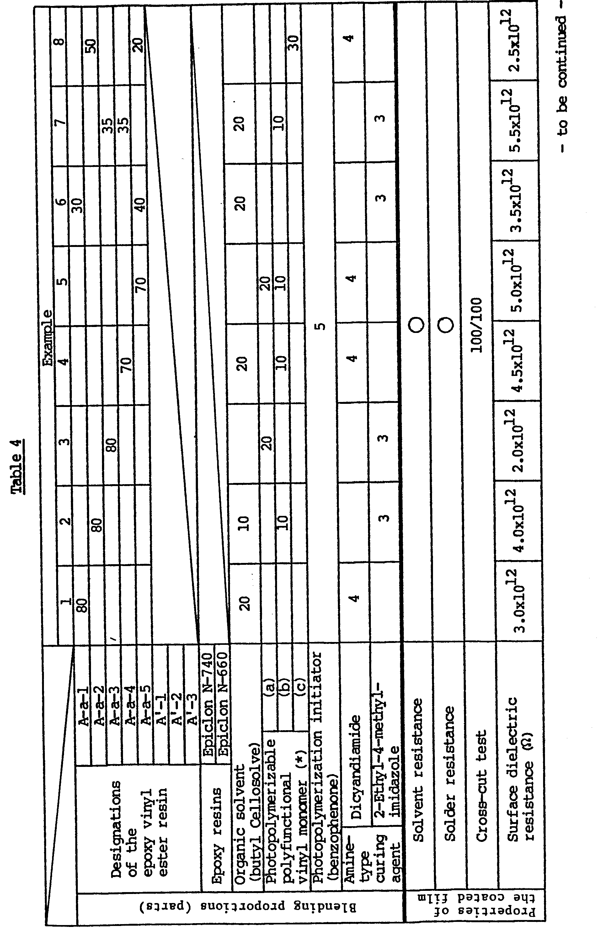
- each of the epoxy vinyl ester resins or epoxy resins obtained ia Referential Examples 1 to 8 was mixed with an organic sovlent or a photopolymerizable polyfunctional vinyl monomer, a photopolymerization initiator, and an amine-type curing agent in the proportions indicated in Table 4 to prepare a solder resist ink.
- the ink was coated to a film thickness of 30 to 40 micrometers on a copper through-hole printed wiring board by screen printing.
- the coated film was dried at 130°C for 5 minutes as required, and exposed to the irradiation of ultraviolet light having an illuminance of 20 mw/cm 2 and a wavelength in the vicinity of 350 nm for 60 seconds through a photomask using a 5 KW ultrahigh voltage mercury lamp. Then, the non-irradiated parts of the coated film were removed by washing it with an organic solvent such as trichloroethylene.
- the wiring board was then heated for 30 minutes at 130°C using a hot air dryer.
- the resulting samples were subjected to the various tests described below.
- Ultraviolet light having a wavelength in the vicinity of 350 nm and an illuminance of 20 mw/cm 2 was irradiated on above coated film for 60 seconds using a 5KW ultrahigh voltage mecury lamp. Then, the unirradi- ated parts were removed by using trichloroethylene, and the state of the coated film at the irradiated parts was observed. Its solvent resistance was evaluated on the following scale.
- solder resistance was evaluated on the following scale.
- the sample resist ink was coated on a test mill pattern in accordance with IPC-840B-25 of the MIL specification, and the substrate was left to stand for 240 hours in an atmosphere kept at a temperature of 85°C and a relative humidity of 95 %.
- the surface dielectric resistance of the coated film was measured in accordance with JIS Z-3197.
Abstract
- (A) an epoxy vinyl ester resin solution obtained by dissolving (A-a) an epoxy vinyl ester resin obtained by the reaction of 1.0 chemical equivalent of a phenol novolak-type epoxy resin and/or a cresol novolak-type epoxy resin with 0.4-to 0.85 chemical equivalent of an unsaturated monobasic acid In (A-b) an organic solvent and/or (A-c) at least one photopolymerizable polyfunctional vinyl monomer selected from the group consisting of trifunctional or higher polyoxyalkylene glycol poly(meth)acrylates, poly(meth)acrylates of polyoxyalkyl isocyanurates and poly(meth)acrylates of acetal compounds,
- (B) a photopolymerization initiator, and
- (C) an amine-type curing agent.
Description
- This invention relates to a new and useful resin composition for use in solder resist ink. More specifically, it relates to a resin composition having excellent heat resistance and dielectric resistance properties for use in printed wiring circuit boards, comprising a vinyl ester resin derived from a specific epoxy resin, a photopolymerization initiator and an amine-type curing agent.
- The present invention provides a resin composition for a liquid photographic image-type solder mask ink. This solder mask ink is used in place of a conventional dry film developing-type solder resist ink to form a resist pattern by coating the liquid photo resist ink on the entire surface of a printed wiring circuit board, exposing the coated film to the irradiation of active energy light through a photomask and then developing the exposed film.
- The solder resist ink is required to have dielectric resistance, heat resistance, adhesion, chemical resistance, screen printability, etc. to avoid its adhesion to unwanted parts and protect the circuit on the printed wiring circuit board in the soldering of parts to the printed circuit board.
- Early in the development of this technology, heat-curable solder resist inks of the melamine resin type were used. Later, heat-curable solder resist inks of the epoxy resin type having superior heat resistance, hardness, adhesion, chemical resistance, etc. were developed and have gained widespread use in printed wiring circuit boards of industrial appliances such as computers that require high reliability.
- On the other hand, since solder resist inks used in printed circuit boards of household appliances require handlability and productivity, ultraviolet- curable solder resist inks based on acrylated epoxy resins or urethane resins have gained widespread acceptance in place of the heat-curable solder resist inks of the epoxy resin type. As is well known, the ultraviolet- curable solder resists are cured by radical reaction induced by the irradiation of ultraviolet light. When a film of the coated resist is thick, curing of its interior is slow. Particularly, in the case of printed circuit boards of industrial appliances, the thickness of conductors is as large as at least 70 micrometers when it is copper-plated or Sn/Pb-plated, the solder resist to be coated on it necessarily has a thickness of at least 50 micrometers in part. Accordingly, parts not irradiated with ultraviolet light, for example, the underside of the edge of the circuit, are not completely cured, and are liable to have low dielectric resistance and permit electro-migration. To prevent such troubles, therefore, it is necessary to adjust the thickness of the resist film to less than 20 micrometers by decreasing the mesh size of the screen and reducing the thickness of the emulsion film. For this reason, the use of the ultraviolet light-curable solder resist inks has been limited to copper conductors in general household appliances on which they may be coated to a thickness of about 35 micrometers. With the recent trend toward size reduction, improved function, material saving, cost curtailment, etc. in the production of electronics devices, the industiral printed circuit boards have also required increased precision in the pattern density of the circuit. Previously, the pattern density was two lines between IC pads, but now 3 to 5 lines between IC pads are desired. With the screen printing process using the existing solder resist inks of the epoxy resin type or ulraviolet light-curable solder resist inks, the dimensional accuracy of the circuit pattern is low because of a limited printing resolution attainable and the stretching of the screen, and no satisfactory results have been obtained.
- The ultraviolet light-curable solder resist ink used in the screen printing process contains mono- to tri-functional monomers such as 2-hydroxyethyl acrylate and trimethylolpropane triacrylate and various acrylate oligomers. These substances migrate during the screen printing, and bring about the serious defect that when such a solder resist ink is used, for example, in a printed wiring circuit board having a pattern density of at least 2 lines between IC pads, soldering cannot be well effected. To prevent this situation, it has been the practice to increase photo resolution by reducing the thickness of the coated film. By such a method, however, the solder resist ink is not uniformly coated on the circult, and the dielectric resistance of the coated film is reduced. The inherent action of the solder resist ink is consequently nullified.
- Recently, a photographic process using a dry film was developed in order to increase photo resolution. This process can certainly give incresed resolution, but the covering property of the dry film between circuits is poor and problems such as the formation of blisters of the coated film or poor film adhesion exist.
- In an attempt to improve the covering property of the dry film between circuits, the development of a liquid photographic image-type solder resist ink has been under way. For example, U. S. Patent No. 4,390,615 discloses a photopolymerizable resin composition comprising a vinyl ester resin obtained by the reaction of nearly equal equivalents of a polyepoxide and an ethylenically unsaturated carboxylic acid, an inert inorganic filler, a photopolymerization initiator and a volatile organic solvent. This photopolymerizable resin composition has good covering property between circuits of a printed circuit board. But since the vinyl ester resin has hardly any epoxide group in the molecule, if a vinyl ester resin obtained by reacting nearly equal equivalents of a phenol novolak-type epoxy resin or a cresol novolak-type epoxy resin with an unsaturated monobasic acid is used in order to increase heat resistance, the resin composition has a poor adhesion to a substrate or low dielectric resistance. Furthermore, if a bisphenol-type epoxy vinyl ester resin is used in order to increase the adhesion to the substrate, the heat resistance or solvent resistance of the resulting composition is poor. Thus, the composition disclosed in the above-cited U. S. Patent is not satisfactory.
- In an attempt to improve the adhesion of the photopolymerizable resin composition disclosed in U. S. Patent No. 4,390,615 to a substrate, one may conceive the preparation of a photopolymerizable resin composition comprising a vinyl ester resin obtained by the reaction of nearly equal equivalents of a polyepoxide and an ethylenically unsaturated carboxylic acid, a photopolymerization initiator, an epoxy resin, a curing agent for the epoxy resin, and a volatile organic solvent. However, when this resin composition is used as a solder resist ink and a resist pattern is formed by exposing a coated film of the ink to active energy light through a photomask and then developing the exposed film, the epoxy resin in the resist ink remains unreacted in the exposed film because the epoxy resin itself is not curable under active energy light. As a result, when the unexposed portions are removed by a solvent such as trichloroethylene, the epoxy resin present in the exposed film is simultaneously dissolved, and a satisfactory coated film cannot be obtained. Hence, the resulting resist pattern is not sharp, and the coated film is markedly reduced in adhesion to a substrate and in heat resistance. Consequently, it is impossible to obtain a solder resist ink of the photographic image type contemplated by the present invention.
- European Patent No. 75537 discloses a resin composition for use in a solder resist ink, comprising a photosensitive epoxy resin composition obtained by the reaction of an epoxy resin with a chalcone group-containing compound such as 4,4'-dihydroxydistyrylketone, bis-(p-hydroxy-benzoinyl vinyl)phenylene or p-hydroxyphenyl-p-hydroxystyrylketone, a curing agent therefor, an organic solvent and a filler. This composition also has the disadvantage of causing reduced dielectric resistance, short-circuiting of a circuit owing to poor soldering, which are attributed to the whitening of the coated film during coating and the formation of small blisters on the coated film during heat curing of the coated film after exposure to active energy light.
- The present inventors have made extensive investigations in view of the various problems in the prior art described above, and have now found that a solder resist ink having superior heat resistance, adhesion, chemical resistance and dielectric resistance can be obtained by using a specific epoxy vinyl ester resin which can be photopolymerized and is curable under heat in the presence of an amine.
- According to this invention, there is provided a resin composition for use in a solder resist ink having excellent heat resistance and resolution in particular, said composition comprising
- (A) an epoxy vinyl ester resin solution obtained by dissolving (A-a) an epoxy vinyl ester resin obtained by the reaction of 1.0 chemical equivalent of a phenol novolak-type epoxy resin and/or a cresol novolak-type epoxy resin with 0.40 to 0.85 chemical equivalent of an unsaturated monobasic acid in (A-b) an organic solvent and/or (A-c) at least one photopolymerizable polyfunctional vinyl monomer selected from the group consisting of trifunctional or higher polyoxyalkylene glycol poly(meth)acrylates, poly(meth)acrylates of polyoxyalkyl
- isocyanurates and poly(meth)acrylates of acetal compounds,
- (B) a photopolymerization initiator, and
- (C) an amine-type curing agent.
- The phenol novolak-type epoxy resin used in this invention denotes a resin which is obtained by reacting a so-called phenol novolak resin derived from phenol and formaldehyde with epichlorohydrin or methylepichlorohydrin. The cresol novolak-type epoxy resin denotes a resin which is obtained by reacting a so-called cresol novolak resin derived from cresol and formaldehyde with epichlorohydrin or methylepichlorohydrin.
- Typical examples of the unsaturated monobasic acid to be reacted with these novolak-type epoxy resins include acrylic acid, methacrylic acid, crotonic acid, monomethyl maleate, monopropyl maleate, monobutyl maleate, sorbic acid, and mono(2-ethylhexyl) maleate. They may be used either singly or in combination.
- The epoxy vinyl ester resin (A-a) can be obtained by reacting the phenol novolak-type epoxy resin and/or cresol novolak-type epoxy resin with the unsaturated monobasic acid in the presence of an esterification catalyst at a temperature of usually 60 to 140°C, prefer- alby 80 to 120°C. In this reaction, the unsaturated monobasic acid is suitably used in a proportion of 0.40 to 0.85 chemical equivalent per 1.0 chemical equivalent of the novolak-type epoxy resin.
- Preferably, the resulting phenol novolak-type epoxy resin or cresol novolak-type epoxy resin is of such a type that the unsaturated monobasic acid adds to some of the epoxy groups and both the epoxy groups and the vinyl groups exist together in one molecule.
- The esterification catalyst may be selected from known conventional esterification catalysts. Typical examples include tertiary amines such as triethylamine, N,N-dimethylbenzylamine, N,N-dimethylaniline or diazabicyclooctane, diethylamine hydrochloride, dimethylamine acetate and dimethylamine nitrate.
- In the preparation of the vinyl ester resin (A-a), the use of a polymerization inhibitor is recommended in order to prevent gellation or to adjust the storage stability or curability of the resulting resin.
- Typical examples of the polymerization inhibit or include hydroquinones such as hydroquinone, p-tert-butylcatechol or mono-tert-butyl hydroquinone; phenols such as hydroquinone monomethyl ether or di-tert-butyl-p-cresol; quinones such as p-benzoquinone, naphthoquinone and p-toluquinone; and copper salts such as copper naphthenate.
- The resulting vinyl ester resin (A-2) is then dissolved in the specific organic solvent (A-b) and/or the photopolymerizable polyfunctional vinyl monomer (A-c) to form a stable resin solution. Typical examples of the organic solvent (A-b) include aromatic hydrocarbons such as toluene or xylene; alcohols such as methanol or isopropanol; esters such as ethyl acetate or butyl acetate; ethers such as 1,4-dioxane or tetrahydrofuran; ketones such as methyl ethyl ketone or methyl isobutyl ketone; glycol derivatives such as Cellosolve or butyl Cellosolve; alicyclic hydrocarbons such as cyclohexanone or cyclohexanol; and petroleum-type solvents such as petroleum naphtha. These solvents may be used singly or in combination. The amount of the organic solvent (A-b) is not particularly restricted, but from the standpoint of handlability, its suitable amount is in the range of 5 to 60 % by weight, preferably 10 to 40 % by weight, based on the epoxy vinyl ester resin (A-a).
- Examples of suitable photopolymerizable vinyl monomers (A-c) from the viewpoint of photocurability or heat resistance include trifunctional or higher polyoxyalkylene glycol poly(meth)acrylates, typified by a tri-, tetra-, penta- or hexa-(meth)acrylate of dipentaerythri- tor, tol, a tri-, tetra-, penta- or hexa-(meth)acrylate of a caprolactone adduct of dipentaerythritol, a tri-(meth)acrylate of a propylene oxide adduct of glycerol, a tri(meth)acrylate of a propylene oxide adduct of trimethylolpropane, or tri- to penta-functional monomers obtained by reacting dipentaerythritol with lower fatty acids having 1 to 4 carbon atoms and (meth)acryllic acid; poly(meth)acrylates of polyoxyalkyl isocyanurates typified by bisl(meth)acrloyloxyethyllhydroxyethyl isocyanurate or trist(meth)acryloyloxyethyll isocyanurate; and poly(meth)acrylates of acetal compounds typified by 2-(2-hydroxy-l,l-dimethylethyl)-5-hydroxymethyl-5-ethyl-1,3-dioxane diacrylate. These monomers may be used singly or in combination.
- The amount of the polyfunctional vinyl monomer (A-c) is not particularly restricted, but from the viewpoint of handlability, its suitable amount is in the range of 5 to 60 % by weight, preferably 10 to 40 % by weight, based on the epoxy vinyl ester resin (A-2).
- Typical examples of the photopolymerizable initiator (B) are carbonyl compounds such as p-tert-butyl- trichloroacetophenone, 2,2-diethoxyacetophenone, benzophenone, 4,4-bismethylaminobenzophenone, benzil, benzoin, benzoin methyl ether, benzoin isobutyl ether, benzil methyl ketal, methyl-o-benzoylbenzoate and alpha-hydroxy- isobutylphenone; sulfur compounds such as tetramethyl- thiuram monosulfide, thioxanthone and 2-chlorothioxan- thone; and azo compounds such as azobisisovaleronitrile. These compounds may be used singly or in combination. The suitable amount of the initiator (B) is in the range of 0.1 to 20 parts by weight per 100 parts by weight of the epoxy vinyl ester resin solution (A).
- Typical examples of the amine-type curing agent (C) include aliphatic polyamines such as ethylenediamine, diethylenetriamine, triethylenetetramine, diethylaminopropylamine and xylylenediamine; aromatic polyamines such as m-phenylenediamine, diaminodiphenylmethane and diaminodiphenylsulfone; alicyclic polyamines such as menthanedi- amine, isophoronediamine and bis(4-amino-3-methylcyclohexyl)methane; dicyandiamide; imidazoles such as 2-methylimidazole, 2-ethyl-4-methylimidazole and l-benzyl-2-methylimidazole; tertiary amines such as benzyl dimethylamine, tridimethylaminomethylphenol and dimethylaminomethyl phenol; and amine complexes such as BF3-monoethylamine.
- Among these, curing agents which have low reactivity at room temperature but can react abruptly when heated are preferred in order to obtain a resist ink having good handlability and a long pot life. The use of the aromatic polyamines, imidazoles, tertiary amines and dicyandiamide is especially preferred.
- In order to improve the various properties of the solder resist ink, the resin composition of this invention may further contain a filler such as silica, talc or clay, a thixotropic agent such as Aerosil, a defoamer or a levelling agent of the silicon or fluorine- type, a coloring agent, etc.
- The resulting resin composition for use in a solder resist ink in accordance with the present invention is coated on the entire surface of a printed circuit board by known conventional methods, for example by screen printing, roll coating or curtain coating.
- When the composition of this invention contains the organic solvent (A-b), it is desirable to render the ink-coated surface tack-free by removing the solvent after a solder resist ink from the composition has been coated and pre-dried. A photomask is brought into intimate contact with the ink-coated surface kept tack-free, and active energy light is irradiated on it to insolubilize the ink by radical polymerization. If the ink surface is not rendered tack-free, a method may be employed in which the photomask is not kept in intimate contact with the ink-coated surface, but the photomask is held on a transparent support, parallel rays of active energy light are irradiated.
- Those parts which have not been exposed to active energy light are removed by washing with a developing solvent such as trichloroethylene, perchloroethylene, methylene chloride, or alkaline water. Thereafter, the epoxy groups present in the epoxy vinyl ester resin (A-a) are reacted by heating to form a cured resist pattern.
- The following Referential Examples, Examples and Comparative Examples specifically illustrate the present invention. Unless otherwise specified, all parts and percentages are by weight.
- Preparation of an epoxy vinyl ester resin for comparison:-
- A three-necked flask equipped with a thermometer, a stirrer and a condenser tube was charged with 1,800 parts (corresponding to 10 epoxy groups) of "Epiclon N-740" (a trade name for a phenol novolak-type epoxy resin produced by Dainippon Ink & Chemicals, Inc.; epoxy equivalent=180), 720 parts (corresponding to 10 carboxyl groups) of acrylic acid, 1.26 parts of hydroquinone and 10.1 parts of triethylamine, and the flask was heated to 110°C. The mixture was maintained at this temperature for 6 hours to give a resin having an acid value of 2.0 and an epoxy equivalent of more than 20,000. The resulting resin is designated as resin (A'-1).
- Preparation of epoxy vinyl ester resins (A-2):-
- Referential Example 1 was repeated except that the proportions of "Epiclon N-740", acrylic acid, hydroquinone and triethylamine used were changed as shown in Table 1.
- The epoxy equivaletns and acid values of the resulting esins (A-a-2) to (A-a-4) are summarized in Table 1.

- Preparation of epoxy vinyl ester resins (A-2):-
- Referential Example 1 was repeated except that the proportions of "Epiclon N-660" (a trade name for a cresol novolak-type epoxy resin manufactured by Ddinippon Ink & Chemicals, Inc.; epoxy equivalent=220) was used instead of "Epiclon N-740", and the proportions of acrylic acid hydroquinoene and triethylamine were changed as shown in Table 2.

- Preparation of epoxy vinyl esters resins for comparison:-
- Referential Example 1 was repeated except that "Epiclon 850" (a trade name for a bisphenol A-type epoxy resin manufactured by Dainippon Ink & Chemicals, Inc.; epoxy equivalent=185) or "Epiclon 1050" (a trade name for a bisphenol A-type epoxy resin manufactured by Dainippon Ink & Chemicals, Inc.; epoxy equivalent=470) was used instead of "Epiclon N-740", and the proportions of acrylic acid, hydroquinone and triethylamine used were changed as shown in Table 3. The properties of the resulting resins are shown in Table 3.

- In each run, each of the epoxy vinyl ester resins or epoxy resins obtained ia Referential Examples 1 to 8 was mixed with an organic sovlent or a photopolymerizable polyfunctional vinyl monomer, a photopolymerization initiator, and an amine-type curing agent in the proportions indicated in Table 4 to prepare a solder resist ink. The ink was coated to a film thickness of 30 to 40 micrometers on a copper through-hole printed wiring board by screen printing.
- The coated film was dried at 130°C for 5 minutes as required, and exposed to the irradiation of ultraviolet light having an illuminance of 20 mw/cm2 and a wavelength in the vicinity of 350 nm for 60 seconds through a photomask using a 5 KW ultrahigh voltage mercury lamp. Then, the non-irradiated parts of the coated film were removed by washing it with an organic solvent such as trichloroethylene.
- The wiring board was then heated for 30 minutes at 130°C using a hot air dryer. The resulting samples were subjected to the various tests described below.
- The results are summarized in Table 4.
- The various properies were evaluated by the following methods.
- Ultraviolet light having a wavelength in the vicinity of 350 nm and an illuminance of 20 mw/cm2 was irradiated on above coated film for 60 seconds using a 5KW ultrahigh voltage mecury lamp. Then, the unirradi- ated parts were removed by using trichloroethylene, and the state of the coated film at the irradiated parts was observed. Its solvent resistance was evaluated on the following scale.
- 0 ..... No change in the appearance of the coated film
- X ..... Dissolved or swollen
- The sample was immersed for 2 minutes in molten solder (composed of 60% of tin and 40% of lead) at 260°C, and the state of the coated film was observed. Its solder resistance was evaluated on the following scale.
- 0 ..... No change in the appearance of the coated film
- X ..... Blisters occurred, or the film was melted, and/or peeled.
- One hundred crosscuts having a size of 1 x 1 mm were formed on the coated film of the sample. A cellophane tape was applied to the cut surface and then peeled. The number of the remaining crosscuts was determined and defined as adhesion. This test was in accordance with JIS D-0202.
- The sample resist ink was coated on a test mill pattern in accordance with IPC-840B-25 of the MIL specification, and the substrate was left to stand for 240 hours in an atmosphere kept at a temperature of 85°C and a relative humidity of 95 %. The surface dielectric resistance of the coated film was measured in accordance with JIS Z-3197.
- The results shown in Table 4 clearly demonstrate that the coated films obtained by using the resin compositions of this invention had excellent heat resistance, adhesion, solvent resistance and dielectric resistance.

Claims (12)
Applications Claiming Priority (8)
| Application Number | Priority Date | Filing Date | Title |
|---|---|---|---|
| JP143268/85 | 1985-06-29 | ||
| JP60143268A JPH0689284B2 (en) | 1985-06-29 | 1985-06-29 | Curable resin composition for solder-resist ink |
| JP143269/85 | 1985-06-29 | ||
| JP14326985A JPS624391A (en) | 1985-06-29 | 1985-06-29 | Resin composition for solder resist ink |
| JP14577985A JPH0689285B2 (en) | 1985-07-04 | 1985-07-04 | Curable resin composition for solder-resist ink |
| JP145778/85 | 1985-07-04 | ||
| JP14577885A JPS627773A (en) | 1985-07-04 | 1985-07-04 | Resin composition for solder resist ink |
| JP145779/85 | 1985-07-04 |
Publications (3)
| Publication Number | Publication Date |
|---|---|
| EP0207188A2 true EP0207188A2 (en) | 1987-01-07 |
| EP0207188A3 EP0207188A3 (en) | 1988-08-17 |
| EP0207188B1 EP0207188B1 (en) | 1996-06-19 |
Family
ID=27472510
Family Applications (1)
| Application Number | Title | Priority Date | Filing Date |
|---|---|---|---|
| EP85111307A Expired - Lifetime EP0207188B1 (en) | 1985-06-29 | 1985-09-06 | Resin composition for solder resist ink |
Country Status (3)
| Country | Link |
|---|---|
| US (1) | US4888269A (en) |
| EP (1) | EP0207188B1 (en) |
| DE (1) | DE3588111T2 (en) |
Cited By (8)
| Publication number | Priority date | Publication date | Assignee | Title |
|---|---|---|---|---|
| EP0246467A2 (en) * | 1986-04-28 | 1987-11-25 | Tokyo Ohka Kogyo Co., Ltd. | Photosensitive resin composition and use thereof |
| EP0273729A2 (en) * | 1986-12-26 | 1988-07-06 | Kabushiki Kaisha Toshiba | Solder resist ink composition |
| EP0346486A1 (en) * | 1987-12-18 | 1989-12-20 | Nippon Kayaku Kabushiki Kaisha | Resin composition and solder resist resin composition |
| EP0381900A2 (en) * | 1989-02-06 | 1990-08-16 | Somar Corporation | Method of forming electrically conducting layer |
| US4996132A (en) * | 1987-02-25 | 1991-02-26 | Toyko Ohka Kogyo Co. Ltd. | Heat-resistant photosensitive resin composition |
| WO1991009068A1 (en) * | 1989-12-08 | 1991-06-27 | Coates Brothers Plc | Curable materials |
| US5215863A (en) * | 1987-12-18 | 1993-06-01 | Nippon Kayaku Kabushiki Kaisha | Resin composition and solder resist composition |
| WO2012084569A1 (en) * | 2010-12-21 | 2012-06-28 | Elantas Gmbh | Epoxy resin compositions containing epoxy and vinyl ester groups |
Families Citing this family (21)
| Publication number | Priority date | Publication date | Assignee | Title |
|---|---|---|---|---|
| WO1988009454A1 (en) * | 1987-05-22 | 1988-12-01 | Kabushiki Kaisha Komatsu Seisakusho | Lockup clutch control apparatus and method |
| JP2573661B2 (en) * | 1988-07-09 | 1997-01-22 | キヤノン株式会社 | Photosensitive adhesive |
| DE69130691T2 (en) * | 1990-08-02 | 1999-07-22 | Ppg Industries Inc | Photosensitive, electrodepositable photoresist composition |
| US5268256A (en) * | 1990-08-02 | 1993-12-07 | Ppg Industries, Inc. | Photoimageable electrodepositable photoresist composition for producing non-tacky films |
| US6329475B1 (en) * | 1992-08-12 | 2001-12-11 | The Dow Chemical Company | Curable epoxy vinylester composition having a low peak exotherm during cure |
| KR0126118B1 (en) * | 1992-09-10 | 1997-12-18 | 다나카 쇼소 | A solder resist ink composition |
| US5854313A (en) * | 1994-09-28 | 1998-12-29 | Takeda Chemical Industries, Ltd. | Fine particles of high heat resistant polymer and epoxy esters |
| WO1996028485A1 (en) * | 1995-03-16 | 1996-09-19 | Ashland Inc. | Low epoxy value vinylesters containing a copper salt inhibitor |
| US6217987B1 (en) * | 1996-11-20 | 2001-04-17 | Ibiden Co. Ltd. | Solder resist composition and printed circuit boards |
| JP3489369B2 (en) * | 1997-01-31 | 2004-01-19 | 松下電器産業株式会社 | Electronic components using cockroach repellent-containing electronic component materials |
| JP4081217B2 (en) * | 1999-03-17 | 2008-04-23 | 互応化学工業株式会社 | UV curable resin composition, photo solder resist ink, pre-dried film, substrate and printed wiring board |
| US7794918B2 (en) * | 2005-12-28 | 2010-09-14 | Fujifilm Corporation | Ink composition, inkjet recording method, printed material, method for producing planographic printing plate, and planographic printing plate |
| JP5339626B2 (en) * | 2008-01-30 | 2013-11-13 | 三菱製紙株式会社 | Method for producing conductive pattern |
| DE102011017708A1 (en) * | 2011-04-28 | 2012-10-31 | Elantas Gmbh | Resin composition containing sorbic acid ester |
| WO2013054317A1 (en) | 2011-10-09 | 2013-04-18 | Hewlett-Packard Industrial Printing Ltd. | Photo-curable ink composition |
| US8703385B2 (en) | 2012-02-10 | 2014-04-22 | 3M Innovative Properties Company | Photoresist composition |
| US8715904B2 (en) | 2012-04-27 | 2014-05-06 | 3M Innovative Properties Company | Photocurable composition |
| EP2666832B1 (en) | 2012-05-22 | 2018-10-10 | HP Scitex Ltd | Photo-curable ink composition |
| US8883402B2 (en) | 2012-08-09 | 2014-11-11 | 3M Innovative Properties Company | Photocurable compositions |
| JP6469006B2 (en) | 2012-08-09 | 2019-02-13 | スリーエム イノベイティブ プロパティズ カンパニー | Photocurable composition |
| US10080287B2 (en) * | 2012-09-27 | 2018-09-18 | Dell Products L.P. | Blind via printed circuit board fabrication supporting press fit connectors |
Citations (12)
| Publication number | Priority date | Publication date | Assignee | Title |
|---|---|---|---|---|
| US3551246A (en) * | 1967-07-10 | 1970-12-29 | Sun Chemical Corp | Radiation curable compositions |
| US3753720A (en) * | 1972-01-10 | 1973-08-21 | Grace W R & Co | Solder resistant photopolymer compositions |
| US3932401A (en) * | 1974-01-31 | 1976-01-13 | Minnesota Mining And Manufacturing Company | Mixed acrylic acid/methacrylic acid esters of tris (hydroxyalkyl) isocyanurates |
| GB2032939A (en) * | 1978-11-01 | 1980-05-14 | Coates Brothers & Co | Coating Compositions |
| US4390615A (en) * | 1979-11-05 | 1983-06-28 | Courtney Robert W | Coating compositions |
| EP0095182A2 (en) * | 1982-05-24 | 1983-11-30 | Hitachi, Ltd. | Photosensitive resin composition |
| EP0106641A1 (en) * | 1982-10-18 | 1984-04-25 | Minnesota Mining And Manufacturing Company | Polymerizable composition for information carrying systems |
| EP0113409A2 (en) * | 1983-01-07 | 1984-07-18 | International Business Machines Corporation | Method and composition for applying coatings on printed circuit boards, and process for making said composition |
| EP0125862A2 (en) * | 1983-05-09 | 1984-11-21 | Asahi Kasei Kogyo Kabushiki Kaisha | Photopolymerizable laminate |
| EP0138209A2 (en) * | 1983-10-14 | 1985-04-24 | Hitachi, Ltd. | Epoxy resin composition |
| US4544623A (en) * | 1981-09-17 | 1985-10-01 | Ciba-Geigy Corporation | Photosensitive coating composition and the use thereof for protective purposes |
| DE3508820A1 (en) * | 1984-02-20 | 1986-09-18 | Toyo Boseki K.K., Osaka | Light-sensitive composition or preparation for an image reproduction material |
Family Cites Families (3)
| Publication number | Priority date | Publication date | Assignee | Title |
|---|---|---|---|---|
| DE2406400B2 (en) * | 1973-02-14 | 1977-04-28 | Hitachi Chemical Co., Ltd., Tokio | LIGHT-SENSITIVE RESIN COMPOSITIONS ON THE BASIS OF COMPOUNDS WITH EPOXY OR. PHOTOPOLYMERIZABLE ACRYLIC GROUPS |
| US4169732A (en) * | 1978-01-09 | 1979-10-02 | International Business Machines Corporation | Photosensitive coating composition and use thereof |
| US4237216A (en) * | 1978-12-08 | 1980-12-02 | International Business Machines Corporation | Photosensitive patternable coating composition containing novolak type materials |
-
1985
- 1985-09-06 EP EP85111307A patent/EP0207188B1/en not_active Expired - Lifetime
- 1985-09-06 DE DE3588111T patent/DE3588111T2/en not_active Expired - Fee Related
-
1988
- 1988-08-11 US US07/231,606 patent/US4888269A/en not_active Expired - Fee Related
Patent Citations (12)
| Publication number | Priority date | Publication date | Assignee | Title |
|---|---|---|---|---|
| US3551246A (en) * | 1967-07-10 | 1970-12-29 | Sun Chemical Corp | Radiation curable compositions |
| US3753720A (en) * | 1972-01-10 | 1973-08-21 | Grace W R & Co | Solder resistant photopolymer compositions |
| US3932401A (en) * | 1974-01-31 | 1976-01-13 | Minnesota Mining And Manufacturing Company | Mixed acrylic acid/methacrylic acid esters of tris (hydroxyalkyl) isocyanurates |
| GB2032939A (en) * | 1978-11-01 | 1980-05-14 | Coates Brothers & Co | Coating Compositions |
| US4390615A (en) * | 1979-11-05 | 1983-06-28 | Courtney Robert W | Coating compositions |
| US4544623A (en) * | 1981-09-17 | 1985-10-01 | Ciba-Geigy Corporation | Photosensitive coating composition and the use thereof for protective purposes |
| EP0095182A2 (en) * | 1982-05-24 | 1983-11-30 | Hitachi, Ltd. | Photosensitive resin composition |
| EP0106641A1 (en) * | 1982-10-18 | 1984-04-25 | Minnesota Mining And Manufacturing Company | Polymerizable composition for information carrying systems |
| EP0113409A2 (en) * | 1983-01-07 | 1984-07-18 | International Business Machines Corporation | Method and composition for applying coatings on printed circuit boards, and process for making said composition |
| EP0125862A2 (en) * | 1983-05-09 | 1984-11-21 | Asahi Kasei Kogyo Kabushiki Kaisha | Photopolymerizable laminate |
| EP0138209A2 (en) * | 1983-10-14 | 1985-04-24 | Hitachi, Ltd. | Epoxy resin composition |
| DE3508820A1 (en) * | 1984-02-20 | 1986-09-18 | Toyo Boseki K.K., Osaka | Light-sensitive composition or preparation for an image reproduction material |
Cited By (15)
| Publication number | Priority date | Publication date | Assignee | Title |
|---|---|---|---|---|
| EP0246467A3 (en) * | 1986-04-28 | 1988-04-20 | Tokyo Ohka Kogyo Co., Ltd. | Photosensitive resin composition and use thereof |
| EP0246467A2 (en) * | 1986-04-28 | 1987-11-25 | Tokyo Ohka Kogyo Co., Ltd. | Photosensitive resin composition and use thereof |
| EP0273729A2 (en) * | 1986-12-26 | 1988-07-06 | Kabushiki Kaisha Toshiba | Solder resist ink composition |
| EP0273729A3 (en) * | 1986-12-26 | 1989-07-12 | Kabushiki Kaisha Toshiba | Solder resist ink composition |
| US4925773A (en) * | 1986-12-26 | 1990-05-15 | Kabushiki Kaisha Toshiba | Solder resist ink composition |
| US4996132A (en) * | 1987-02-25 | 1991-02-26 | Toyko Ohka Kogyo Co. Ltd. | Heat-resistant photosensitive resin composition |
| EP0346486A4 (en) * | 1987-12-18 | 1991-12-27 | Nippon Kayaku Kabushiki Kaisha | Resin composition and solder resist resin composition |
| EP0346486A1 (en) * | 1987-12-18 | 1989-12-20 | Nippon Kayaku Kabushiki Kaisha | Resin composition and solder resist resin composition |
| US5215863A (en) * | 1987-12-18 | 1993-06-01 | Nippon Kayaku Kabushiki Kaisha | Resin composition and solder resist composition |
| EP0381900A2 (en) * | 1989-02-06 | 1990-08-16 | Somar Corporation | Method of forming electrically conducting layer |
| EP0381900A3 (en) * | 1989-02-06 | 1992-04-15 | Somar Corporation | Method of forming electrically conducting layer |
| WO1991009068A1 (en) * | 1989-12-08 | 1991-06-27 | Coates Brothers Plc | Curable materials |
| WO2012084569A1 (en) * | 2010-12-21 | 2012-06-28 | Elantas Gmbh | Epoxy resin compositions containing epoxy and vinyl ester groups |
| US20140018472A1 (en) * | 2010-12-21 | 2014-01-16 | Elantas Gmbh | Epoxy resin compositions comprising epoxy and vinyl ester groups |
| US10381129B2 (en) * | 2010-12-21 | 2019-08-13 | Elantas Gmbh | Epoxy resin compositions comprising epoxy and vinyl ester groups |
Also Published As
| Publication number | Publication date |
|---|---|
| DE3588111D1 (en) | 1996-07-25 |
| EP0207188A3 (en) | 1988-08-17 |
| US4888269A (en) | 1989-12-19 |
| DE3588111T2 (en) | 1996-10-31 |
| EP0207188B1 (en) | 1996-06-19 |
Similar Documents
| Publication | Publication Date | Title |
|---|---|---|
| EP0207188B1 (en) | Resin composition for solder resist ink | |
| EP0323563B1 (en) | Photosensitive thermosetting resin composition and method of forming solder resist pattern by use thereof | |
| US6238841B1 (en) | Photosensitive resin composition and photoresist ink for manufacturing printed wiring boards | |
| JP3455296B2 (en) | Spacer material for touch panel and touch panel using the same | |
| JPH05339356A (en) | Photopolymerizable unsaturated compound, and photosensitive resin composition of alkali development type | |
| US5246816A (en) | Cationic electrodeposition negative type resist composition | |
| EP0362735B1 (en) | Unsaturated group-containing polycarboxylic acid resin, resin composition and solder resist resin composition comprising the same and cured product thereof | |
| US5858618A (en) | Photopolymerizable resinous composition | |
| JPH05204150A (en) | Photosensitive resin composition and production of photosensitive element and platable resist | |
| JP2003280192A (en) | Photosetting and thermosetting resin composition | |
| US5468784A (en) | Photopolymerizable resin composition | |
| JPH0122312B2 (en) | ||
| JPH05341521A (en) | Photosensitive resin composition and manufacture of photosensitive element and plated resist by using same | |
| EP0573053A1 (en) | Photo-curable and thermosetting coating composition and method for formation of solder resist pattern | |
| JPH04195043A (en) | Photosensitive composition and production of printed circuit board with solder resist using the same | |
| JP2002040647A (en) | Resist ink composition | |
| JPS61201237A (en) | Photosensitive resin composition | |
| JPH0882930A (en) | Photosetting and thermosetting resin composition | |
| JP2963069B2 (en) | Solder photoresist ink composition | |
| JPH06332169A (en) | Resist ink composition | |
| JPS61130946A (en) | Photosensitive resin composition | |
| JPH0689285B2 (en) | Curable resin composition for solder-resist ink | |
| JP2001264977A (en) | Photosensitive resin composition | |
| JP2695359B2 (en) | Photosensitive resin composition and use | |
| JPH0720631A (en) | Photosensitive thermosetting resin composition and method for forming solder mask |
Legal Events
| Date | Code | Title | Description |
|---|---|---|---|
| PUAI | Public reference made under article 153(3) epc to a published international application that has entered the european phase |
Free format text: ORIGINAL CODE: 0009012 |
|
| AK | Designated contracting states |
Kind code of ref document: A2 Designated state(s): CH DE FR GB LI SE |
|
| PUAL | Search report despatched |
Free format text: ORIGINAL CODE: 0009013 |
|
| AK | Designated contracting states |
Kind code of ref document: A3 Designated state(s): CH DE FR GB LI SE |
|
| 17P | Request for examination filed |
Effective date: 19890208 |
|
| 17Q | First examination report despatched |
Effective date: 19891127 |
|
| GRAH | Despatch of communication of intention to grant a patent |
Free format text: ORIGINAL CODE: EPIDOS IGRA |
|
| GRAH | Despatch of communication of intention to grant a patent |
Free format text: ORIGINAL CODE: EPIDOS IGRA |
|
| GRAA | (expected) grant |
Free format text: ORIGINAL CODE: 0009210 |
|
| AK | Designated contracting states |
Kind code of ref document: B1 Designated state(s): CH DE FR GB LI SE |
|
| PG25 | Lapsed in a contracting state [announced via postgrant information from national office to epo] |
Ref country code: FR Effective date: 19960619 |
|
| REG | Reference to a national code |
Ref country code: CH Ref legal event code: NV Representative=s name: BOVARD AG PATENTANWAELTE |
|
| REF | Corresponds to: |
Ref document number: 3588111 Country of ref document: DE Date of ref document: 19960725 |
|
| PG25 | Lapsed in a contracting state [announced via postgrant information from national office to epo] |
Ref country code: SE Effective date: 19960919 Ref country code: GB Effective date: 19960919 |
|
| PG25 | Lapsed in a contracting state [announced via postgrant information from national office to epo] |
Ref country code: LI Effective date: 19960930 Ref country code: CH Effective date: 19960930 |
|
| EN | Fr: translation not filed | ||
| PLBE | No opposition filed within time limit |
Free format text: ORIGINAL CODE: 0009261 |
|
| STAA | Information on the status of an ep patent application or granted ep patent |
Free format text: STATUS: NO OPPOSITION FILED WITHIN TIME LIMIT |
|
| GBPC | Gb: european patent ceased through non-payment of renewal fee |
Effective date: 19960919 |
|
| REG | Reference to a national code |
Ref country code: CH Ref legal event code: PL |
|
| PG25 | Lapsed in a contracting state [announced via postgrant information from national office to epo] |
Ref country code: DE Effective date: 19970603 |
|
| 26N | No opposition filed |