EP0204377A2 - Digitising television signals - Google Patents
Digitising television signals Download PDFInfo
- Publication number
- EP0204377A2 EP0204377A2 EP86200963A EP86200963A EP0204377A2 EP 0204377 A2 EP0204377 A2 EP 0204377A2 EP 86200963 A EP86200963 A EP 86200963A EP 86200963 A EP86200963 A EP 86200963A EP 0204377 A2 EP0204377 A2 EP 0204377A2
- Authority
- EP
- European Patent Office
- Prior art keywords
- signal
- arrangement
- analogue
- television
- digital converter
- Prior art date
- Legal status (The legal status is an assumption and is not a legal conclusion. Google has not performed a legal analysis and makes no representation as to the accuracy of the status listed.)
- Withdrawn
Links
Images

Classifications
-
- H—ELECTRICITY
- H04—ELECTRIC COMMUNICATION TECHNIQUE
- H04N—PICTORIAL COMMUNICATION, e.g. TELEVISION
- H04N17/00—Diagnosis, testing or measuring for television systems or their details
- H04N17/02—Diagnosis, testing or measuring for television systems or their details for colour television signals
Definitions
- the invention relates to an arrangement for digitising television signals, which signals comprise a luminance portion whose amplitude changes at a relatively low frequency and a high frequency colour subcarrier portion, said arrangement comprising a first and second analogue to digital converter, means for separating the luminance and colour subcarrier portions, means for applying the separated luminance portion to the first analogue to digital converter, and means for applying the separated colour subcarrier portion to the second analogue to digital converter.
- the invention further relates to an arrangement for measuring television signals and to a television transmitter.
- Broadcasting authorities generally require their transmitters to meet certain requirements concerning the quality of the transmitted signals.
- linearity and differential gain With the growing use of computers for analysing signals it becomes desirable to digitise the television signals to make them convenient to handle.
- both the British Broadcasting Corporation and the Independent Broadcasting Authority insert test signals into certain lines of the television signal during the field blanking period. These signals include a portion which includes a luminance portion having a staircase form on each step of which a constant amplitude colour subcarrier wave is superimposed. This can be used to measure three important non-linear distortions, i.e. luminance non-linearity, differential gain, and differential phase.
- this signal is converted directly to a digital representation then in order to satisfy the Nyquist Criterion it must be sampled at a rate greater than twice the video signal bandwidth, i.e. faster than 11 MHz in the UK. In practice the analysis is easier to carry out if the sampling rate is four times the colour subcarrier frequency ( - 17.7MHz).
- the digitisation must also be very accurate since any error in the conversion process will cause a much larger error in the calculated values of luminance non-linearity and differential gain.lf these parameters need to be measured to within about 1% then a 10 bit analogue to digital converter is required. The combination of high speed of operation and high accuracy is expensive.
- the invention provides an arrangement for digitising television signals as set forth in the opening paragraph characterised in that the colour sub- carrier signal has a relatively low peak value compared with that of the total television signal and the second analogue to digital converter has a lower resolution and a higher speed of operation than the first analogue to digital converter.
- the invention is based on the recognition of the fact that the most important parameters which have to be monitored can be determined by analysis of the staircase portion of the test signal and that by separating the two components of the staircase and separately digitising them it is possible to maintain the full speed and accuracy without the use of an analogue to digital converter having both a high speed of operation and high resolution.
- the second analogue to digital converter may operate at an integral multiple of the colour sub- carrier frequency, which multiple may be four.
- the operating frequency of the first analogue to digital converter may be 1/2" of that of the second analogue to digital converter, where n is a positive integer greater than one and may be four.
- the arrangement may further comprise means for writing the outputs of the first and second analogue to digital converters into a store.
- the arrangement may further comprise means for writing the outputs of the analogue to digital converters into the store only during a selected portion of the lines on which the test signal is transmitted.
- the invention further provides an arrangement for measuring the distortion of television signals transmitted by a television transmitter comprising means for receiving the transmitted signal, means for demodulating the transmitted signal, means for digitising the demodulated signal, means for analysing the digitised signal, and means for displaying the measured distortion characterised in that the means for digitising the demodulated signal comprises an arrangement for digitising television signals according to the invention.
- the invention still further relates to a television transmitter comprising a video signal input; means for modulating a carrier signal by the video signal; non-linear power amplifier means for amplifying the modulated carrier signal; a pre-corrector circuit for applying a correction to the video signal before or after modulation and before it is applied to the power amplifier means; means for measuring the distortion at the output of the power amplifying means; means for generating a control signal representative of the distortion of the output of the power amplifying means; and means for applying the control signal to a control input of the pre-corrector circuit to reduce the distortion at the output of the power amplifying means; wherein the measuring means comprises means for extracting a portion of the transmitted signal, and means for demodulating the portion to produce a demodulated television signal, characterised in that the measuring means further comprises means for digitising the demodulated television signal, the digitising means comprising an arrangement for digitising a television signal according to the invention.
- the television transmitter may comprise means for transmitting a test signal in a television line during the field or frame blanking interval, means for selecting the line in which the test signal is transmitted, and means for applying at least a part of the selected line to the measuring means.
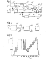
- the arrangement for digitising television signals shown in Figure 1 has an input 1 for receiving an analogue television signal, the input 1 being connected to the input of a luminance/chrominance separator 2.
- the luminance/chrominance separator 2 may comprise a band pass and a low pass filter to separate a high frequency chrominance portion from a low frequency luminance portion as exists in the staircase portion of the test signal shown in Figure 5.
- the signal amplitude V between values 0 and 1.0 is plotted versus the time t in ⁇ s.
- the chrominance portion is fed from a first output 3 of the separator 2 to a first input 4 of a timing generator 5 and to the analogue signal input of an analogue-to-digital converter (ADC) 6.
- ADC analogue-to-digital converter
- the luminance portion is fed from a second output 7 of the separator 2 to a second input 8 of the timing generator 5 and to the analogue signal input of a further analogue-to-digital converter (ADC) 9.
- ADC analogue-to-digital converter
- the digital signal output of the ADC 6 is fed over a path 10 to a block of random access memory (RAM) 11.
- RAM random access memory
- the digital signal output of the ADC 9 is fed over a path 12 to a block of RAM
- a further output of the ADC 6 is connected, over a line 15, to an input of a write control circuit 14 whose output ' is fed to the RAM 11 over a line 16.
- a further output of the ADC 9 is connected to an input of a further write control circuit 17 over a line 18, the output of the further write control circuit 17 being fed to a RAM 13 over a line 19.
- a terminal 20 is connected via a line 21 to further inputs of the write control circuits 14 and 17.
- a first output of the timing generator 5 is connected via a line 22 to a further input of the ADC 6, a second output of the timing generator 5 is connected via a line 23 to a further input of the ADC 9, a third output of the timing generator 5 is connected via a line 24 to an input of a write address generator 25, and a fourth output of the timing generator 5 is connected to further inputs of the write control circuits 14 and 17 via a line 26.
- the output of the write address generator 25 is connected to the RAM 11 via a path 27 and to the RAM 13 via a path 28 An output of the RAM 11 is fed to a terminal 29 via a path 30, while an output of the RAM 13 is fed to a terminal 31 via a path 32.
- a terminal 33 is connected to an input of a read address generator 34 whose output is connected to the RAM 11 via a path 35 and to the RAM 13 ' via a path 36.
- a television signal is fed to the input I and when a test signal of the form shown in Figure 5 is included in a given line of a field or frame the timing generator 5 produces appropriate signals from the line and field synchronising pulses to select the line on which the test signal is transmitted.
- the luminance/chrominance separator 2 separates the low amplitude, high frequency colour sub-carrier portion from the high amplitude, low frequency luminance portion of the signal.
- the separated colour sub-carrier portion from output 3 of the separator 2 is fed to the input of the ADC 6 which in this embodiment is a 7 bit ADC which is capable of operating at four times the colour sub- carrier frequency (- 17.7MHz for the PAl. System I signal).
- the digitised samples are then stored in the RAM 11 under the control of the write address generator 25 and the write control circuit 14.
- the write control circuit 14 produces a write enable signal on line 16 under the control of a data ready signal produced by the ADC 6 and fed over line 15 and a timing signal generated by the timing gener- . ator 5 and fed over line 26.
- the timing generator 5 indicates that the appropriate television line and portion of that line is being received and the ADC 6 indicates that the signal has been digitised and that the digital representation of a particular sample is available at the output of the ADC 6.
- the timing generator 5 also produces a 4( sc clock on line 24 which causes the write address generator to increment at that rate so that successive samples available at the output of the ADC 6 are stored at successive locations of the RAM 11.
- the luminance portion of the television signal which is produced at the output 7 of the separator 2 is fed to the input of the ADC 9 which in this embodiment is a 10 bit ADC capable of operating at about IMHz (conveniently 17.7/16MHz).
- the digitised luminance samples are stored in the RAM 13 under the control of the write control circuit 17 and write address generator 25.
- the write control circuit 17 produces a write enable signal for the RAM 13 on line 19 from similar signals to those applied to the write control circuit 14, the difference being that the data ready signal is taken from the ADC 9 over the line 18.
- the addresses to the RAM 13 may, conveniently, be the same as those applied to the RAM 11 with the four least significant bits deleted. Thus the addresses to the RAM 13 will change at one sixteenth of the rate at which the addresses to the RAM 11 change.
- the clock signal to the ADC 6 over line 22 will also be at sixteen times the rate of the clock signal to the ADC 9 over line 23.
- the read address generator 34 is incremented by signals applied to terminal 33. Information is read from the RAMs 11 and 13 under the control of the read address generator 34. Again the four least significant bits of the output of the read address generator 34 are not applied to the RAM 13 as only one sixteenth of the number of samples are stored in the RAM 13. The outputs from the RAMs 11 and 13 are fed to outputs 29 and 31 where they are available separately. Alternatively they could be combined in an adding arrangement to produce a digital version of the input signal, the most significant bit of the colour sub-carrier signal being a sign bit.
- FIG 2 shows an embodiment of a timing generator suitable for use as the timing generator 5 of Figure 1.
- the input 4 of the timing generator is fed to a clock generator 50 which generates a clock signal at four times the colour subcarrier signal (4 fsc ).
- the input 8 of the timing generator is fed to the input of a synchronising signal separator 51 which may be of conventional form and which produces a burst gate signal on a line 52 which is fed to a further input of the clock generator 50, field or frame synchronising pulses on a line 53 which are fed to a line counter 54 and line synchronising pulses on a line 55 which are fed to an element counter 56.
- the 4 fsc output of the clock generator 50 is fed via a line 57 to a further input of the element counter 56, a line 58 to a first input of an AND gate 59, a line 60 to the input of a binary divider 61, and a line 62 to an output terminal 63.
- the output of the element counter 56 is fed via a line 64 to a further input of the line counter 54.
- the output of the line counter 54 is fed to the set input of a bistable circuit 70 while the line synchronising pulses are fed via a line 71 to the reset input of the bistable 70.
- the Q output of the bistable 70 is fed to a second input of the AND gate 59 so that the AND gate 59 is enabled when the bistable 70 is set.
- the output of the line counter 54 is also fed to an output terminal 65.
- the output of the counter 61 is fed to an output terminal 66 while the output of the AND gate 61 is fed to an output terminal 67.
- the clock generator 50 comprises an oscillator having a nominal frequency of 4 fsc which is phase- locked to the input colour sub-carrier signal on terminal 4 using the burst gate signal produced by the synchronising signal separator 51 and applied over line 52.
- the line counter 54 is preset by the frame or field synchronising signal on line 53 and is incremented by the line synchronising signal delayed by the element counter 56 on the line ZD 64. Thus a signal is produced at terminal 65 when a given portion of a given line is reached. This signal is passed over line 26 to the write control circuits 14 and 17 to enable them to produce write enable signals for the RAMs 11 and 13.
- the element counter 56 is preset by the line synchronising signals and incremented by the 4 fsc clock signals.
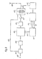
- Figure 3 shows in block schematic form a television transmitter employing adaptive pre-correction.
- the Klystron is normally driven into a non-linear region of its characteristic as close to saturation as possible.
- the pre-correctors have a fixed characteristic which is designed to be the inverse of the Klystron characteristic.
- the degree to which the Klystron is driven into saturation is increased so the demands made on the pre-correction is increased and in order to meet the specifications set by the Broadcasting authorities it is becoming necessary to improve the accuracy of the pre-correction.
- the transmitter shown in Figure 3 employs adaptive pre-correction, i.e. the characteristics of the pre-correction circuits are modified in dependence on the distortion measured at the output of the Klystron amplifier.
- the transmitter has an input 100 to which a composite video signal is applied and which is connected to the input of a video processing circuit 101.
- the video processing circuit 101 strips the synchronising pulses from the composite video signal and provides a first output signal comprising the synchronising pulses which is connected via a line 102 to an anode pulser in a Klystron amplifier 103.
- the video processing circuit 101 also produces a second output signal comprising the composite video signal minus the synchronising pulses, the second output signal being fed to a modulator 104.
- the output of the modulator 104 is fed to the input of a pre-corrector circuit 105 whose output is fed to an up-converter 106.
- the output of the up-converter 106 is fed via a preamplifying stage 107 to an input of the Klystron amplifier 103.
- the output of the Klystron amplifier 103 is fed to a transmitting aerial 108.
- a probe 109 taps a small portion of the output of the Klystron amplifier 103, the small portion being fed to the input of a demodulator 110 which produces the demodulated composite video signal at its output.
- the output of the demodulator 110 is fed to a digitiser 111 which in this embodiment comprises an arrangement as shown in Figure 1.
- the output of the digitiser 111 is fed via a data bus 112 to a control unit 113 while control signals are fed from the control unit 113 to the digitiser 111 over a data bus 114.
- the control unit 113 produces control signals which are fed to the pre-corrector circuit 105 via a bus 115.
- the control unit 113 will typically comprise a microcomputer including suitable interface circuitry. Such control units are known to workers skilled in the art as evidenced by the measurement systems discussed in the introduction of this specification and as disclosed in UK patent application No. 8423440 (PHB33117) the contents of which are hereby incorporated by reference.
- the pre-corrector circuit 105 may be substantially as disclosed in that UK patent application.
- the Klystron amplifier 103 is operated as near to saturation as possible in order to increase the efficiency and the synchronising pulses are used to switch the beam current to a higher value during the synchronising period only.
- the pre-corrector circuit 105 is made adjustable so that the degree of pre-correction can be controlled to produce the best possible performance.
- the control unit 113 takes the digitised video signal and analyses the distortion. It then produces appropriate control signals for application to the pre-corrector circuit 105 to produce a pre-correction characteristic which minimises the distortion of the output signal.
- the control unit 113 provides signals to the digitiser 111 which enable the contents of the RAMs 11 and 13 to be read at a rate at which the control unit is able to absorb and act upon them. This can be independent of the input information rate by appropriate use of the signal applied to the read address generator 34.
- Figure 4 shows an arrangement for measuring the distortion of a television signal.
- the arrangement has an input 200 for receiving a composite video signal for analysis.
- the arrangement may additionally include a demodulator for demodulating a television signal produced at the output of a transmitter and, if necessary, a probe for extracting a portion of the signal from the output of the transmitter.
- the input 200 is connected to a digitiser 201 which may be in the form of an arrangement as shown in Figure 1.
- the output of the digitiser 201 is fed to a control unit 202 via a bus 203 while outputs of the control unit 202 are fed via a bus 204 to further inputs of the digitiser 201. Further outputs of the control unit 202 are fed to a display device 205 via a bus 206.
- a composite video signal is fed to the input of the digitiser 201 and stored therein.
- the stored samples are read by the control unit 202 and analysed and the results of the analysis are fed to -the display device 205.
- the analysis may be carried out in a conventional manner in the control unit 202 which may comrise a microcomputer.
- the design of such computer based control units is known to those skilled in the art as evidenced by commercially available measuring instruments such as those referred to hereinbefore.
- the display device may be a video display unit or may be a printer to provide hard copy results. Intermediate storage may be included between the control unit and display device to enable measurements to be made on site and the results to be displayed at a central location.
Abstract
Description
- The invention relates to an arrangement for digitising television signals, which signals comprise a luminance portion whose amplitude changes at a relatively low frequency and a high frequency colour subcarrier portion, said arrangement comprising a first and second analogue to digital converter, means for separating the luminance and colour subcarrier portions, means for applying the separated luminance portion to the first analogue to digital converter, and means for applying the separated colour subcarrier portion to the second analogue to digital converter. The invention further relates to an arrangement for measuring television signals and to a television transmitter.
- Broadcasting authorities generally require their transmitters to meet certain requirements concerning the quality of the transmitted signals. Among the more important parameters that have to be monitored or controlled are linearity and differential gain. With the growing use of computers for analysing signals it becomes desirable to digitise the television signals to make them convenient to handle. In the UK both the British Broadcasting Corporation and the Independent Broadcasting Authority insert test signals into certain lines of the television signal during the field blanking period. These signals include a portion which includes a luminance portion having a staircase form on each step of which a constant amplitude colour subcarrier wave is superimposed. This can be used to measure three important non-linear distortions, i.e. luminance non-linearity, differential gain, and differential phase. If this signal is converted directly to a digital representation then in order to satisfy the Nyquist Criterion it must be sampled at a rate greater than twice the video signal bandwidth, i.e. faster than 11 MHz in the UK. In practice the analysis is easier to carry out if the sampling rate is four times the colour subcarrier frequency ( - 17.7MHz). The digitisation must also be very accurate since any error in the conversion process will cause a much larger error in the calculated values of luminance non-linearity and differential gain.lf these parameters need to be measured to within about 1% then a 10 bit analogue to digital converter is required. The combination of high speed of operation and high accuracy is expensive.
- There are a variety of methods which allow the signal to be digitised in a_ less expensive manner. but all the known methods tend to degrade the speed, accuracy or susceptability to noise of the arrangement. One method, which is used in the Tektronix Automatic Video Measurement Set 1980 Answer, is to use a high speed reduced resolution analogue to digital converter and to add a dither signal to the analogue video input. The full resolution is eventually obtained by averaging the resultant digital signal over many repeated occurances of the test signal. Another method, which is used in the Thomson-CSF TTV 8400 System, is to use a low speed full resolution analogue to digital converter and to build up a complete replica of the test signal by taking a few samples from each of successive test signals. This is however a slow process which is susceptable to noise.
- It is an object of the invention to enable the digitisation of video signals to be carried out in an alternative manner which mitigates at least some of the disadvantages referred to hereinbefore.
- The invention provides an arrangement for digitising television signals as set forth in the opening paragraph characterised in that the colour sub- carrier signal has a relatively low peak value compared with that of the total television signal and the second analogue to digital converter has a lower resolution and a higher speed of operation than the first analogue to digital converter.
- The invention is based on the recognition of the fact that the most important parameters which have to be monitored can be determined by analysis of the staircase portion of the test signal and that by separating the two components of the staircase and separately digitising them it is possible to maintain the full speed and accuracy without the use of an analogue to digital converter having both a high speed of operation and high resolution.
- The second analogue to digital converter may operate at an integral multiple of the colour sub- carrier frequency, which multiple may be four.
- By sampling at four times the colour sub-carrier frequency (- 17.7MHz for the PAL System I signal) the subsequent signal processing can be simplified.
- The operating frequency of the first analogue to digital converter may be 1/2" of that of the second analogue to digital converter, where n is a positive integer greater than one and may be four.
- This enables a simple binary divider to be used to generate the clock for the first analogue to digital converter from the clock applied to the second analogue to digital converter.
- The arrangement may further comprise means for writing the outputs of the first and second analogue to digital converters into a store.
- An arrangement in which the television signal comprises a test signal for transmission on one or more lines of each television field or frame may be characterised in that the arrangement comprises
- means for selecting the line or lines in which the test signal is transmitted and writing the outputs of the analogue to digital converters into the store only on those lines.
- The arrangement may further comprise means for writing the outputs of the analogue to digital converters into the store only during a selected portion of the lines on which the test signal is transmitted.
- The invention further provides an arrangement for measuring the distortion of television signals transmitted by a television transmitter comprising means for receiving the transmitted signal, means for demodulating the transmitted signal, means for digitising the demodulated signal, means for analysing the digitised signal, and means for displaying the measured distortion characterised in that the means for digitising the demodulated signal comprises an arrangement for digitising television signals according to the invention.
- The invention still further relates to a television transmitter comprising a video signal input; means for modulating a carrier signal by the video signal; non-linear power amplifier means for amplifying the modulated carrier signal; a pre-corrector circuit for applying a correction to the video signal before or after modulation and before it is applied to the power amplifier means; means for measuring the distortion at the output of the power amplifying means; means for generating a control signal representative of the distortion of the output of the power amplifying means; and means for applying the control signal to a control input of the pre-corrector circuit to reduce the distortion at the output of the power amplifying means; wherein the measuring means comprises means for extracting a portion of the transmitted signal, and means for demodulating the portion to produce a demodulated television signal, characterised in that the measuring means further comprises means for digitising the demodulated television signal, the digitising means comprising an arrangement for digitising a television signal according to the invention.
- The television transmitter may comprise means for transmitting a test signal in a television line during the field or frame blanking interval, means for selecting the line in which the test signal is transmitted, and means for applying at least a part of the selected line to the measuring means.
- Embodiments of the invention will now be described, by way of example, with reference to the accompanying drawings, in which:-
- Figure 1 shows in block schematic form an arrangement for digitising television signals according to the invention,
- Figure 2 shows in greater detail the timing generator of Figure 1,
- Figure 3 shows in block schematic form a television transmitter according to the invention,
- Figure 4 shows in block schematic form an arrangement for measuring the distortion of television signals according to the invention, and
- Figure 5 shows an insertion test signal which the arrangement of Figure 1 may be used to digitise.
- The arrangement for digitising television signals shown in Figure 1 has an
input 1 for receiving an analogue television signal, theinput 1 being connected to the input of a luminance/chrominance separator 2. The luminance/chrominance separator 2 may comprise a band pass and a low pass filter to separate a high frequency chrominance portion from a low frequency luminance portion as exists in the staircase portion of the test signal shown in Figure 5. In Figure 5 the signal amplitude V between values 0 and 1.0 is plotted versus the time t in µs. The chrominance portion is fed from a first output 3 of the separator 2 to a first input 4 of a timing generator 5 and to the analogue signal input of an analogue-to-digital converter (ADC) 6. The luminance portion is fed from asecond output 7 of the separator 2 to a second input 8 of the timing generator 5 and to the analogue signal input of a further analogue-to-digital converter (ADC) 9. The digital signal output of the ADC 6 is fed over a path 10 to a block of random access memory (RAM) 11. Similarly the digital signal output of the ADC 9 is fed over apath 12 to a block of RAM A further output of the ADC 6 is connected, over aline 15, to an input of awrite control circuit 14 whose output ' is fed to theRAM 11 over aline 16. Similarly a further output of the ADC 9 is connected to an input of a furtherwrite control circuit 17 over aline 18, the output of the furtherwrite control circuit 17 being fed to aRAM 13 over aline 19. Aterminal 20 is connected via aline 21 to further inputs of thewrite control circuits line 22 to a further input of the ADC 6, a second output of the timing generator 5 is connected via aline 23 to a further input of the ADC 9, a third output of the timing generator 5 is connected via aline 24 to an input of awrite address generator 25, and a fourth output of the timing generator 5 is connected to further inputs of thewrite control circuits line 26. The output of thewrite address generator 25 is connected to theRAM 11 via apath 27 and to theRAM 13 via apath 28 An output of theRAM 11 is fed to aterminal 29 via apath 30, while an output of theRAM 13 is fed to aterminal 31 via apath 32. Aterminal 33 is connected to an input of aread address generator 34 whose output is connected to theRAM 11 via apath 35 and to theRAM 13 'via apath 36. - In operation a television signal is fed to the input I and when a test signal of the form shown in Figure 5 is included in a given line of a field or frame the timing generator 5 produces appropriate signals from the line and field synchronising pulses to select the line on which the test signal is transmitted. The luminance/chrominance separator 2 separates the low amplitude, high frequency colour sub-carrier portion from the high amplitude, low frequency luminance portion of the signal. The separated colour sub-carrier portion from output 3 of the separator 2 is fed to the input of the ADC 6 which in this embodiment is a 7 bit ADC which is capable of operating at four times the colour sub- carrier frequency (- 17.7MHz for the PAl. System I signal). The digitised samples are then stored in the
RAM 11 under the control of thewrite address generator 25 and thewrite control circuit 14. Thewrite control circuit 14 produces a write enable signal online 16 under the control of a data ready signal produced by the ADC 6 and fed overline 15 and a timing signal generated by the timing gener- . ator 5 and fed overline 26. Thus in order to produce the write enable signal for theRAM 11 the timing generator 5 indicates that the appropriate television line and portion of that line is being received and the ADC 6 indicates that the signal has been digitised and that the digital representation of a particular sample is available at the output of the ADC 6. The timing generator 5 also produces a 4(sc clock online 24 which causes the write address generator to increment at that rate so that successive samples available at the output of the ADC 6 are stored at successive locations of theRAM 11. - The luminance portion of the television signal which is produced at the
output 7 of the separator 2 is fed to the input of the ADC 9 which in this embodiment is a 10 bit ADC capable of operating at about IMHz (conveniently 17.7/16MHz). The digitised luminance samples are stored in theRAM 13 under the control of thewrite control circuit 17 and writeaddress generator 25. Thewrite control circuit 17 produces a write enable signal for theRAM 13 online 19 from similar signals to those applied to thewrite control circuit 14, the difference being that the data ready signal is taken from the ADC 9 over theline 18. The addresses to theRAM 13 may, conveniently, be the same as those applied to theRAM 11 with the four least significant bits deleted. Thus the addresses to theRAM 13 will change at one sixteenth of the rate at which the addresses to theRAM 11 change. The clock signal to the ADC 6 overline 22 will also be at sixteen times the rate of the clock signal to the ADC 9 overline 23. - The
read address generator 34 is incremented by signals applied toterminal 33. Information is read from theRAMs address generator 34. Again the four least significant bits of the output of the readaddress generator 34 are not applied to theRAM 13 as only one sixteenth of the number of samples are stored in theRAM 13. The outputs from theRAMs outputs - Figure 2 shows an embodiment of a timing generator suitable for use as the timing generator 5 of Figure 1. The input 4 of the timing generator is fed to a clock generator 50 which generates a clock signal at four times the colour subcarrier signal (4fsc). The input 8 of the timing generator is fed to the input of a synchronising signal separator 51 which may be of conventional form and which produces a burst gate signal on a
line 52 which is fed to a further input of the clock generator 50, field or frame synchronising pulses on aline 53 which are fed to aline counter 54 and line synchronising pulses on aline 55 which are fed to anelement counter 56. The 4fsc output of the clock generator 50 is fed via aline 57 to a further input of theelement counter 56, aline 58 to a first input of an ANDgate 59, aline 60 to the input of abinary divider 61, and aline 62 to anoutput terminal 63. The output of theelement counter 56 is fed via aline 64 to a further input of theline counter 54. The output of theline counter 54 is fed to the set input of abistable circuit 70 while the line synchronising pulses are fed via aline 71 to the reset input of the bistable 70. The Q output of the bistable 70 is fed to a second input of the ANDgate 59 so that the ANDgate 59 is enabled when the bistable 70 is set. The output of theline counter 54 is also fed to an output terminal 65. The output of thecounter 61 is fed to anoutput terminal 66 while the output of the ANDgate 61 is fed to anoutput terminal 67. - The clock generator 50 comprises an oscillator having a nominal frequency of 4 fsc which is phase- locked to the input colour sub-carrier signal on terminal 4 using the burst gate signal produced by the synchronising signal separator 51 and applied over
line 52. Theline counter 54 is preset by the frame or field synchronising signal online 53 and is incremented by the line synchronising signal delayed by theelement counter 56 on theline ZD 64. Thus a signal is produced at terminal 65 when a given portion of a given line is reached. This signal is passed overline 26 to thewrite control circuits RAMs element counter 56 is preset by the line synchronising signals and incremented by the 4fsc clock signals. Consequently it produces an output at line frequency which can be delayed by a period which depends on the state to which it is preset and which can be arranged to cause the line counter to increment just prior to the staircase portion of the test signal, i.e. approximately 321lsecs after the start of the synchronising pulse. As a result a signal is produced at terminal 65 just prior to the staircase portion of the test signal to allow that portion to be stored in theRAMs gate 59 is enabled and clock pulses at the 4fsc rate are produced atterminal 67 and passed vialine 24 to thewrite address generator 25 to cause the write address generator to increment and store the digitised samples at successive locations in theRAMs output terminal 63 and is applied overline 22 to the ADC 6. The 4fsc clock signal is divided by sixteen in thedivider 61 and the resultant 1/4 fsc clock signal is applied overline 23 to the ADC 9. - Figure 3 shows in block schematic form a television transmitter employing adaptive pre-correction. In order to increase the electrical power efficiency of a transmitter which employs a Klystron amplifier as the power output stage the Klystron is normally driven into a non-linear region of its characteristic as close to saturation as possible. As a result it is necessary to pre-correct the signal applied to the Klystron amplifier to limit the distortion at the output of the amplifier. Conventionally the pre-correctors have a fixed characteristic which is designed to be the inverse of the Klystron characteristic. However, as the degree to which the Klystron is driven into saturation is increased so the demands made on the pre-correction is increased and in order to meet the specifications set by the Broadcasting Authorities it is becoming necessary to improve the accuracy of the pre-correction.
- The transmitter shown in Figure 3 employs adaptive pre-correction, i.e. the characteristics of the pre-correction circuits are modified in dependence on the distortion measured at the output of the Klystron amplifier. The transmitter has an
input 100 to which a composite video signal is applied and which is connected to the input of avideo processing circuit 101. Thevideo processing circuit 101 strips the synchronising pulses from the composite video signal and provides a first output signal comprising the synchronising pulses which is connected via a line 102 to an anode pulser in a Klystron amplifier 103. Thevideo processing circuit 101 also produces a second output signal comprising the composite video signal minus the synchronising pulses, the second output signal being fed to amodulator 104. The output of themodulator 104 is fed to the input of apre-corrector circuit 105 whose output is fed to an up-converter 106. The output of the up-converter 106 is fed via apreamplifying stage 107 to an input of the Klystron amplifier 103. The output of the Klystron amplifier 103 is fed to a transmitting aerial 108. Aprobe 109 taps a small portion of the output of the Klystron amplifier 103, the small portion being fed to the input of ademodulator 110 which produces the demodulated composite video signal at its output. The output of thedemodulator 110 is fed to adigitiser 111 which in this embodiment comprises an arrangement as shown in Figure 1. The output of thedigitiser 111 is fed via a data bus 112 to acontrol unit 113 while control signals are fed from thecontrol unit 113 to thedigitiser 111 over adata bus 114. - The
control unit 113 produces control signals which are fed to thepre-corrector circuit 105 via abus 115. Thecontrol unit 113 will typically comprise a microcomputer including suitable interface circuitry. Such control units are known to workers skilled in the art as evidenced by the measurement systems discussed in the introduction of this specification and as disclosed in UK patent application No. 8423440 (PHB33117) the contents of which are hereby incorporated by reference. Thepre-corrector circuit 105 may be substantially as disclosed in that UK patent application. - The Klystron amplifier 103 is operated as near to saturation as possible in order to increase the efficiency and the synchronising pulses are used to switch the beam current to a higher value during the synchronising period only. As a result the degree of distortion in the video signal produced by running the Klystron near to saturation is high and significant pre-correction is required to meet the specification. The
pre-corrector circuit 105 is made adjustable so that the degree of pre-correction can be controlled to produce the best possible performance. Thecontrol unit 113 takes the digitised video signal and analyses the distortion. It then produces appropriate control signals for application to thepre-corrector circuit 105 to produce a pre-correction characteristic which minimises the distortion of the output signal. - The
control unit 113 provides signals to thedigitiser 111 which enable the contents of theRAMs address generator 34. - Figure 4 shows an arrangement for measuring the distortion of a television signal. The arrangement has an
input 200 for receiving a composite video signal for analysis. Alternatively the arrangement may additionally include a demodulator for demodulating a television signal produced at the output of a transmitter and, if necessary, a probe for extracting a portion of the signal from the output of the transmitter. Theinput 200 is connected to adigitiser 201 which may be in the form of an arrangement as shown in Figure 1. The output of thedigitiser 201 is fed to acontrol unit 202 via abus 203 while outputs of thecontrol unit 202 are fed via abus 204 to further inputs of thedigitiser 201. Further outputs of thecontrol unit 202 are fed to adisplay device 205 via abus 206. - In operation a composite video signal is fed to the input of the
digitiser 201 and stored therein. The stored samples are read by thecontrol unit 202 and analysed and the results of the analysis are fed to -thedisplay device 205. The analysis may be carried out in a conventional manner in thecontrol unit 202 which may comrise a microcomputer. The design of such computer based control units is known to those skilled in the art as evidenced by commercially available measuring instruments such as those referred to hereinbefore. The display device may be a video display unit or may be a printer to provide hard copy results. Intermediate storage may be included between the control unit and display device to enable measurements to be made on site and the results to be displayed at a central location.
Claims (12)
Applications Claiming Priority (2)
| Application Number | Priority Date | Filing Date | Title |
|---|---|---|---|
| GB08514152A GB2176669A (en) | 1985-06-05 | 1985-06-05 | Digitising television signals |
| GB8514152 | 1985-06-05 |
Publications (2)
| Publication Number | Publication Date |
|---|---|
| EP0204377A2 true EP0204377A2 (en) | 1986-12-10 |
| EP0204377A3 EP0204377A3 (en) | 1989-01-18 |
Family
ID=10580195
Family Applications (1)
| Application Number | Title | Priority Date | Filing Date |
|---|---|---|---|
| EP86200963A Withdrawn EP0204377A3 (en) | 1985-06-05 | 1986-06-03 | Digitising television signals |
Country Status (5)
| Country | Link |
|---|---|
| US (1) | US4729011A (en) |
| EP (1) | EP0204377A3 (en) |
| JP (1) | JPS61280192A (en) |
| ES (1) | ES8800539A1 (en) |
| GB (1) | GB2176669A (en) |
Cited By (1)
| Publication number | Priority date | Publication date | Assignee | Title |
|---|---|---|---|---|
| EP3223520A4 (en) * | 2014-11-19 | 2018-01-17 | Sanechips Technology Co., Ltd. | Measurement method and apparatus for composite video broadcast signal quality and storage medium |
Families Citing this family (6)
| Publication number | Priority date | Publication date | Assignee | Title |
|---|---|---|---|---|
| US5325187A (en) * | 1988-04-27 | 1994-06-28 | Canon Kabushiki Kaisha | Image processing apparatus with back porch period sampling and clamping |
| GB2258969A (en) * | 1991-08-21 | 1993-02-24 | British Broadcasting Corp | Decoding of composite television signals |
| US6188518B1 (en) | 1993-01-22 | 2001-02-13 | Donald Lewis Maunsell Martin | Method and apparatus for use in producing three-dimensional imagery |
| KR0176502B1 (en) * | 1995-01-28 | 1999-04-15 | 김광호 | Method for obtaining a stabilized slow function in the vtr and apparatus for carrying on the method |
| US6278743B1 (en) * | 1996-11-12 | 2001-08-21 | Zenith Electronics Corporation | Non linear amplitude precorrection for HDTV transmitter |
| US7483037B2 (en) * | 2005-10-27 | 2009-01-27 | Apple, Inc. | Resampling chroma video using a programmable graphics processing unit to provide improved color rendering |
Citations (5)
| Publication number | Priority date | Publication date | Assignee | Title |
|---|---|---|---|---|
| US4215367A (en) * | 1974-11-01 | 1980-07-29 | Independent Broadcasting Authority | Television systems |
| EP0104681A2 (en) * | 1982-08-31 | 1984-04-04 | Philips Patentverwaltung GmbH | Circuit arrangement for converting an analogous colour video signal into a digital signal |
| DE3339030A1 (en) * | 1982-10-29 | 1984-05-03 | Victor Company Of Japan, Ltd., Yokohama, Kanagawa | CIRCUIT ARRANGEMENT FOR DIGITIZING AND STORING VIDEO COLOR SIGNALS |
| DE3435169A1 (en) * | 1983-09-26 | 1985-04-11 | Sony Corp., Tokio/Tokyo | DIGITAL CONVERTER SYSTEM FOR COLOR VIDEO SIGNALS |
| EP0176138A2 (en) * | 1984-09-17 | 1986-04-02 | Philips Electronics Uk Limited | Television transmitter |
Family Cites Families (2)
| Publication number | Priority date | Publication date | Assignee | Title |
|---|---|---|---|---|
| JPS54149515A (en) * | 1978-05-17 | 1979-11-22 | Nec Corp | Separator circuit for luminance signal and chromaticity signal |
| US4531149A (en) * | 1983-06-24 | 1985-07-23 | Rca Corporation | Digital variable group delay equalizer for a digital television receiver |
-
1985
- 1985-06-05 GB GB08514152A patent/GB2176669A/en not_active Withdrawn
-
1986
- 1986-06-02 ES ES555586A patent/ES8800539A1/en not_active Expired
- 1986-06-03 EP EP86200963A patent/EP0204377A3/en not_active Withdrawn
- 1986-06-03 JP JP61127378A patent/JPS61280192A/en active Pending
- 1986-06-05 US US06/871,181 patent/US4729011A/en not_active Expired - Fee Related
Patent Citations (5)
| Publication number | Priority date | Publication date | Assignee | Title |
|---|---|---|---|---|
| US4215367A (en) * | 1974-11-01 | 1980-07-29 | Independent Broadcasting Authority | Television systems |
| EP0104681A2 (en) * | 1982-08-31 | 1984-04-04 | Philips Patentverwaltung GmbH | Circuit arrangement for converting an analogous colour video signal into a digital signal |
| DE3339030A1 (en) * | 1982-10-29 | 1984-05-03 | Victor Company Of Japan, Ltd., Yokohama, Kanagawa | CIRCUIT ARRANGEMENT FOR DIGITIZING AND STORING VIDEO COLOR SIGNALS |
| DE3435169A1 (en) * | 1983-09-26 | 1985-04-11 | Sony Corp., Tokio/Tokyo | DIGITAL CONVERTER SYSTEM FOR COLOR VIDEO SIGNALS |
| EP0176138A2 (en) * | 1984-09-17 | 1986-04-02 | Philips Electronics Uk Limited | Television transmitter |
Cited By (1)
| Publication number | Priority date | Publication date | Assignee | Title |
|---|---|---|---|---|
| EP3223520A4 (en) * | 2014-11-19 | 2018-01-17 | Sanechips Technology Co., Ltd. | Measurement method and apparatus for composite video broadcast signal quality and storage medium |
Also Published As
| Publication number | Publication date |
|---|---|
| US4729011A (en) | 1988-03-01 |
| EP0204377A3 (en) | 1989-01-18 |
| ES555586A0 (en) | 1987-10-16 |
| GB2176669A (en) | 1986-12-31 |
| ES8800539A1 (en) | 1987-10-16 |
| JPS61280192A (en) | 1986-12-10 |
| GB8514152D0 (en) | 1985-07-10 |
Similar Documents
| Publication | Publication Date | Title |
|---|---|---|
| EP0427206A2 (en) | Transmitter phase and amplitude correction for linear FM systems | |
| US3987280A (en) | Digital-to-bandpass converter | |
| US4517520A (en) | Circuit for converting a staircase waveform into a smoothed analog signal | |
| EP0016503A1 (en) | Waveform correction circuit | |
| US4700222A (en) | Apparatus and method of testing the frequency response of a cable television system | |
| EP0204377A2 (en) | Digitising television signals | |
| EP0186521B1 (en) | Digital phase difference detecting circuit | |
| US4377822A (en) | Test equipment for a teletex television receiver | |
| US2753546A (en) | Signal translator | |
| US4354200A (en) | Amplitude modulator circuit for modulating a video signal on a carrier signal | |
| EP0573295B1 (en) | Level detection circuit and automatic color control circuit | |
| EP0343892A1 (en) | Digital FM demodulating apparatus | |
| US4041534A (en) | Automatic distortion correction arrangement | |
| US2949228A (en) | Circuits embodying electronic counters | |
| EP0532702B1 (en) | Digital fm synthesizer for record circuitry | |
| US4833545A (en) | Receiver system of image signal from weather satellite | |
| JPS60107932A (en) | Analog-to-digital converter | |
| US4577217A (en) | Encoding circuit for a SECAM color television transmission | |
| JPS5829910B2 (en) | Image signal correlation processing method | |
| US4760448A (en) | Method of measuring amplitude variations of a video carrier and apparatus therefor | |
| EP0111374A1 (en) | Colour television picture display device | |
| EP0191468B1 (en) | An apparatus for generating a velocity error signal | |
| US4414568A (en) | Device for the measurement, in operation, of non-linearity products in a television transmitter | |
| US3170118A (en) | Panoramic receiver for multiplexing communication signals from multiple sources | |
| US4327372A (en) | Encoding circuit for a secam color television transmitter |
Legal Events
| Date | Code | Title | Description |
|---|---|---|---|
| PUAI | Public reference made under article 153(3) epc to a published international application that has entered the european phase |
Free format text: ORIGINAL CODE: 0009012 |
|
| AK | Designated contracting states |
Kind code of ref document: A2 Designated state(s): DE FR GB |
|
| RAP3 | Party data changed (applicant data changed or rights of an application transferred) |
Owner name: N.V. PHILIPS' GLOEILAMPENFABRIEKEN Owner name: PHILIPS ELECTRONIC AND ASSOCIATED INDUSTRIES LIMIT |
|
| PUAL | Search report despatched |
Free format text: ORIGINAL CODE: 0009013 |
|
| AK | Designated contracting states |
Kind code of ref document: A3 Designated state(s): DE FR GB |
|
| 17P | Request for examination filed |
Effective date: 19890710 |
|
| 17Q | First examination report despatched |
Effective date: 19910626 |
|
| STAA | Information on the status of an ep patent application or granted ep patent |
Free format text: STATUS: THE APPLICATION IS DEEMED TO BE WITHDRAWN |
|
| RAP3 | Party data changed (applicant data changed or rights of an application transferred) |
Owner name: N.V. PHILIPS' GLOEILAMPENFABRIEKEN Owner name: PHILIPS ELECTRONICS UK LIMITED |
|
| 18D | Application deemed to be withdrawn |
Effective date: 19911107 |
|
| RIN1 | Information on inventor provided before grant (corrected) |
Inventor name: MCCANN, KENNETH DAVID |