EP0203601A2 - Cache system adopting an LRU system, and magnetic disk controller incorporating it - Google Patents
Cache system adopting an LRU system, and magnetic disk controller incorporating it Download PDFInfo
- Publication number
- EP0203601A2 EP0203601A2 EP86107284A EP86107284A EP0203601A2 EP 0203601 A2 EP0203601 A2 EP 0203601A2 EP 86107284 A EP86107284 A EP 86107284A EP 86107284 A EP86107284 A EP 86107284A EP 0203601 A2 EP0203601 A2 EP 0203601A2
- Authority
- EP
- European Patent Office
- Prior art keywords
- cache
- data
- read
- disk
- memory
- Prior art date
- Legal status (The legal status is an assumption and is not a legal conclusion. Google has not performed a legal analysis and makes no representation as to the accuracy of the status listed.)
- Granted
Links
Images


Classifications
-
- G—PHYSICS
- G06—COMPUTING; CALCULATING OR COUNTING
- G06F—ELECTRIC DIGITAL DATA PROCESSING
- G06F3/00—Input arrangements for transferring data to be processed into a form capable of being handled by the computer; Output arrangements for transferring data from processing unit to output unit, e.g. interface arrangements
- G06F3/06—Digital input from, or digital output to, record carriers, e.g. RAID, emulated record carriers or networked record carriers
- G06F3/0601—Interfaces specially adapted for storage systems
-
- G—PHYSICS
- G06—COMPUTING; CALCULATING OR COUNTING
- G06F—ELECTRIC DIGITAL DATA PROCESSING
- G06F12/00—Accessing, addressing or allocating within memory systems or architectures
- G06F12/02—Addressing or allocation; Relocation
- G06F12/08—Addressing or allocation; Relocation in hierarchically structured memory systems, e.g. virtual memory systems
- G06F12/0802—Addressing of a memory level in which the access to the desired data or data block requires associative addressing means, e.g. caches
- G06F12/0866—Addressing of a memory level in which the access to the desired data or data block requires associative addressing means, e.g. caches for peripheral storage systems, e.g. disk cache
-
- G—PHYSICS
- G06—COMPUTING; CALCULATING OR COUNTING
- G06F—ELECTRIC DIGITAL DATA PROCESSING
- G06F12/00—Accessing, addressing or allocating within memory systems or architectures
- G06F12/02—Addressing or allocation; Relocation
- G06F12/08—Addressing or allocation; Relocation in hierarchically structured memory systems, e.g. virtual memory systems
- G06F12/12—Replacement control
- G06F12/121—Replacement control using replacement algorithms
- G06F12/126—Replacement control using replacement algorithms with special data handling, e.g. priority of data or instructions, handling errors or pinning
-
- G—PHYSICS
- G06—COMPUTING; CALCULATING OR COUNTING
- G06F—ELECTRIC DIGITAL DATA PROCESSING
- G06F11/00—Error detection; Error correction; Monitoring
- G06F11/07—Responding to the occurrence of a fault, e.g. fault tolerance
- G06F11/14—Error detection or correction of the data by redundancy in operation
- G06F11/1402—Saving, restoring, recovering or retrying
- G06F11/1415—Saving, restoring, recovering or retrying at system level
-
- G—PHYSICS
- G06—COMPUTING; CALCULATING OR COUNTING
- G06F—ELECTRIC DIGITAL DATA PROCESSING
- G06F2212/00—Indexing scheme relating to accessing, addressing or allocation within memory systems or architectures
- G06F2212/31—Providing disk cache in a specific location of a storage system
- G06F2212/312—In storage controller
-
- G—PHYSICS
- G06—COMPUTING; CALCULATING OR COUNTING
- G06F—ELECTRIC DIGITAL DATA PROCESSING
- G06F3/00—Input arrangements for transferring data to be processed into a form capable of being handled by the computer; Output arrangements for transferring data from processing unit to output unit, e.g. interface arrangements
- G06F3/06—Digital input from, or digital output to, record carriers, e.g. RAID, emulated record carriers or networked record carriers
- G06F3/0601—Interfaces specially adapted for storage systems
- G06F3/0628—Interfaces specially adapted for storage systems making use of a particular technique
- G06F3/0655—Vertical data movement, i.e. input-output transfer; data movement between one or more hosts and one or more storage devices
- G06F3/0656—Data buffering arrangements
Definitions
- the present invention relates to a cache system adopting an LRU (Least Recently Used) system in a replacement algorithm for cache blocks, and to a magnetic disk controller incorporating the cache system.
- LRU Least Recently Used
- a disk cache is a memory device using a semiconductor RAM and is designed to eliminate an access gap between a high-speed main memory and low-speed large-capacity secondary memories (i.e., magnetic disk units).
- the disk cache is normally arranged between the main memory and a magnetic disk unit, in a magnetic disk controller, and serves as a data buffer.
- the principle of the disk cache is the same as that of a central processing unit (CPU) cache. If a CPU first accesses part of a file, necessary data blocks are stored on a disk. In this case, the disk cache does not contribute to such CPU access.
- CPU central processing unit
- Necessary blocks are transferred from the disk to the main memory. At the same time, they are written in the disk cache. If the CPU subsequently accesses the same blocks, they are transferred from the disk cache, but not from the disk.
- the access time of the magnetic disk unit is normally 20 to 30 ms, while the access time of the disk cache is about 1 to 3 ms. The access time can, therefore, be decreased to about 1/10.
- a total access time is regarded as an input/output response time including data transfer time and channel wait time, it can be normally decreased to 1/2 to 1/3.
- disk cache mechanism components are a disk cache handler as a program in the input/output controller, a data transfer mechanism between the main memory and the disk cache, and a disk cache directory.
- the disk cache handler cooperates with an operating system (OS) to determine the hit/miss ratio of the disk cache, control of data transfer between the main memory, the disk cache, and the magnetic disks, and acquisition of data representing utilization efficiency of the disk cache and the hit ratio, and so on.
- OS operating system
- Write access schemes include a write through scheme and a write back scheme.
- the write through scheme is called a store through scheme for writing data directory in a disk.
- the cache hit processing is performed in such a way that the cache hit block is disabled by not writing data therein, or the data is written in the cache hit block after it is directly written into the disk.
- the write back scheme is called a store in, copy back, or post store scheme.
- the disk cache write is the highest priority.
- data input/output is completed. If the file is unnecessary or the cache block storing the file must be emptied for other files, data is transferred from the cache to the disk.
- staging data copying from the magnetic disk to the cache memory
- destaging copying from the cache memory to the magnetic disk
- the disk cache replacement algorithm is an LRU algorithm.
- LRU stands for "Least Recently Used.” According to the LRU algorithm, the block which stays in the cache for the longest period after the last access is selected as the least necessary block. In a disk cache having no empty space, if the cache memory must be assigned for new staging, the least necessary track data is removed to obtain an empty space. The LRU algorithm is used to assure this empty space.
- the LRU value in the cache directory corresponding to the hit cache block is initialized to "0".
- the LRU value corresponding to the cache block to be replaced must be registered again.
- the corresponding data block is read out from the magnetic disk unit and is stored in the cache block in the cache memory which is to be replaced.
- LRU setting values are determined regardless of the data blocks stored in the cache memory.
- the frequency of use of the data blocks stored in the cache blocks varies according to different types of files. Once a data block having a low frequency of use is stored in -the cache block, the resident possibility of that data block in the cache memory is often higher than that of a file having a high frequency of use. Because of this, a decrease in hit rate of the cache memory tends to occur.
- disk write operation is always performed in response to a disk write instruction from a host system.
- the conventional system even if the data in the disk area subjected to disk write is stored in the cache memory (even if cache hit occurs), the contents of the cache memory and the disk unit are simultaneously updated. This is not to allow non-updated data to be left in the disk when a failure, such as a power failure, occurs.
- the magnetic disk controller retrieves a disk cache directory (a table having file information such as a file name, a file size, and a file address) and checks if the data block of interest is stored in the disk cache. If cache hit occurs, the corresponding data block is transferred from the cache memory to the main memory.
- a disk cache directory a table having file information such as a file name, a file size, and a file address
- a cache memory is commonly used by, e.g., 4 magnetic disk drives DKO through DK3, different cache memory areas are permanently assigned for respective drives DKO through DK3, and a directory memory having a corresponding memory allocation is prepared, as shown in Fig. 1.
- the limited area of the cache memory is divided, and the cache locations respectively assigned to the magnetic disk drives are decreased, leading to a reduction in the cache hit rate. If the access frequency varies for the different drives, the frequency of use of the cache memory location corresponding to the drive having the lowest access frequency is decreased. As a result, the overall utilization efficiency of the cache memory is degraded.
- a cache system employing an LRU (Least Recently Used) scheme in a replacement algorithm of cache blocks, comprising:
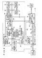
- Fig. 2 is a block diagram showing an embodiment of magnetic disk controller 20 incorporating a disk cache system.
- Hard disk control circuit (to be referred to as an HDC hereinafter) 21 for controlling disk unit 10 is connected to host system 11 through first bus 24, which consists of data line 22 and control line 23, and driver/receiver (to be referred to as a D/R hereinafter) 25.
- HDC 21 is also connected to second bus 26.
- HDC 21 consists of command register 21 1 , ID register 21 2 , and DMA 21 3 .
- Bus 26 is also connected to microprocessor 27 for controlling the overall operation of controller 20, program memory 28 storing control programs (microprograms) for microprocessor 27, work memory 29 used as a work area of microprocessor 27, and buffer memory 30 for compensating a difference between the transfer rates of disk unit 10 and host system 11.
- Third bus 31 is connected to cache control circuit 34, mainly for controlling data transfer, the operation of which includes control of cache memory 33, directory memory/search circuit 35 consisting of directory memory 35 1 and directory search circuit 35 2 , and address stack memory 45.
- Memory 45 is a FIFO (first-in first-out) stack for storing cache operation designation data consisting of three parameters. These three parameters are transfer start cache address a, the number of transfer sectors Q , and data transfer direction control code C.
- the output of stack address counter 46 is connected to address port A of address stack memory 45.
- Bus 26 is connected to the input of counter 46.
- Bus 31 is connected to the input to LRU counter (referred to as an CLRU hereinafter) 36 for storing an LRU value read out from memory 35 1 in the directory search mode, as well as the output of driver 37.
- the output of CLRU 36 and the input of driver 37 are connected to cache control circuit 34.
- Bus 31 is also connected to the input port of register file 38 and the B input of comparator 39.
- the A input of comparator 39 receives the data from bus 31.
- the output port of comparator 39 is connected to control circuit 34.
- Control circuit 34 is connected to register file 38 to control inputs thereto, i.e., the CLRU 36 contents (LRU values) output by driver 37 on bus 31.
- File 38 comprises four registers 50 through 53, i.e., RTCAO through RTCA3.
- the output of directory memory address counter (to be referred to as a CDMA hereinafter) 40 is connected to address port A of directory memory 35 1 to designate the addresses of memory 35 1 .
- the input of CDMA 40 is connected to second bus 26.
- the output of CDMA 40 is connected to the input of register file 41.
- the output of file 41 is also connected to bus 26.
- File 41 is connected through control line 65 so as to receive control signals from cache control circuit 34.
- Register file 41 consists of three registers 60 through 62, i.e., RCGAO through RCGA2.
- Each entry of directory memory 35 1 includes disk block number field (8 bits) 81 representing the number of data blocks registered in cache memory 33, and LRU counter field (8 bits) 83 representing an LRU value, as shown in Fig. 3.
- the number of entries in memory 35 1 is equal to that of cache blocks in cache memory 33. In this embodiment, 16 entries are given for each column.
- One track of disk unit 10 consists of 64 sectors, each corresponding to one block of cache memory 33. The area of disk unit 10 is divided into column 0 and column 1 which store data in units of 64 sectors.
- a column value is represented by the seventh bit from the LSB of a disk logical address (to be described later).
- the disk block number is represented by the MSB excluding the lower seven bits of the disk logical address.
- a read/write command from host'system 11 is stored in command register 21 1 in HDC 21 through D/R 25 and bus 24.
- the read/write command is a 6-byte instruction including command code 85 for designating read/write operation or the like, a disk logical address consisting of logical address 2 (MSB) 87, logical address 1 89, and logical address 0 (LS B ) 91, the number of data blocks, and each field 93 of cache control bits CC2 through CCO (Fig. 4).
- the read/write command in register 21 1 is read out by microprocessor 27 and stored in a predetermined area of work memory 29.
- microprocessor 27 stores the read/write command from host system 11 in memory 29, microprocessor 27 issues a seek command which is then set in command register 21 1 in HDC 21.
- HDC 21 controls disk unit 10 to seek a specified track.
- Microprocessor 27 also sets, in accordance with the read/write command, a disk block number corresponding to the access area of disk unit 10, and an LRU value of "0" in register file 38 through bus 26, D/R 32, and bus 31.
- Microprocessor 27 sets bit 6 of logical address 0 (Fig. 4), i.e., the start address of the currently read-accessed entry in each area (for 16 entries) in directory memory 35 jr in CDMA 40. In this case, each area is accessed by the column value. The following directory search cycle is repeated 16 times.
- CDMA 40 is sequentially counted up.
- Directory data of the entry in directory memory 35 1 is read out onto bus 31 in units of bytes in response to the count from the CDMA 40.
- the readout directory data is supplied to the B input of comparator 39.
- Byte data from register file 38 is supplied to the A input of comparator 39 in response to the data supplied to the B input.
- Comparator 39 compares the contents of the A and B inputs.
- the comparison result of comparator 39 i.e., the result of comparison of the target data block number from file 38 with the registered data block number from memory 35 1 in units of bytes, is supplied to cache control circuit 34.
- the result of comparison between the LRU value from file 38 and that from memory 35 1 is also supplied to cache control circuit 34.
- the LRU value supplied from memory 35 1 to the B input of comparator 39 through bus 31 is supplied to CLRU 36.
- the LRU value stored in CLRU 36 is incremented by one.
- Cache control circuit 34 determines if cache hit occurs according to the data block number comparison result from comparator 39. If circuit 34 determines that coincidence is detected by comparator 39 and cache hit occurs, it appends a cache hit flag to the address set in RCGAO 60 in register file 41, i.e., to the address representing the start position of the entry being searched in the current directory search cycle. The address with a cache hit flag is set in RCGAl 61 in register file 41. Cache control circuit 34 determines the entry of directory memory 35 1 which corresponds to the cache block to be replaced at this time, according to the LRU value comparison result.
- cache control circuit 34 determines that the cache block corresponding to the entry is a candidacy of block to be replaced. Control circuit 34 transfers the address from RCGAO 60 in file 41 to RCGA2 62 therein. Control circuit 34 causes driver 37 to send the incremented LRU value from CLRU 36 onto bus 31. The LRU value in register file 38 is then updated to correspond with that appearing on bus 31. Cache control circuit 34 also writes the LRU value stored in CLRU 36 via bus 31 in the corresponding entry in directory memory 35 1 , regardless of the comparison result of comparator 39. In this embodiment, the LRU value in the corresponding entry in memory 35 1 is incremented by one for each directory search cycle.
- the above operation is the directory search cycle. This cycle is repeated 16 times to complete the directory search corresponding to the given read/write command.
- the start address of the entry in memory 35 1 which corresponds to the hit cache block is set in RCGAl 61 in register file 41.
- the start address of the entry in memory 35 1 which has the largest LRU value in the specified column is stored in RCGA2 62.
- microprocessor 27 fetches the content of RCGA1 61 in file 41 through bus 26, and checks the flag mentioned above in R CG A 1 61 whether cache hit or miss occurs. If microprocessor 27 detects cache hit, the LRU value in the entry in memory 35 1 which is specified by the content (directory address) of RCGA1 61 in file 41 is initialized (or re-registered). However, if the read mode is specified, even if cache miss is detected, the LRU value in the entry in memory 35 1 which is specified by the content of RCGA2 62 in file 41 is initialized (or re-registered).
- microprocessor 27 retrieves the read/write command sent from host system 11 and retained in buffer memory 30.
- the same L RU setting value is supplied to directory memory 35 1 through bus 26, D/R 32, and bus 31, and is registered in LRU counter field 83 of the entry in memory 35 1 .
- the updated LRU setting value is used. If CC1 and CCO are set to be "I”, the resident period of the data block in cache memory 33 can be decreased. However, if CC1 and CCO are set to be "0", the period can be increased.
- Figs. 6 through 12 show another embodiment of a disk cache system wherein the number of write cycles for the disk can be decreased without using an expensive power source, thereby improving system performance.
- Fig. 6 shows a format of directory data stored in directory memory 35 1 .
- Directory data set in each entry in directory memory 35 1 consists of a cache active bit representing whether the content of a block (cache block) in cache memory 33 for a corresponding entry is effective or not, a write command receiving bit representing whether the write data specified by host system 11 is completely written in disk unit 10 or not, a resident bit representing whether replacement of the cache block corresponding to this entry is inhibited, a disk address (disk block address) of a data block (disk block) stored in cache memory 33, and a replacement counter (replacement counter value) used for replacement operation.
- Fig. 7 shows a format of a disk write instruction sent from host system 11 to disk controller 20.
- the write instruction includes a specified write instruction designation bit for determining whether the write instruction is the specified write instruction which allows data write in cache memory 33 but does not require data write in disk unit 10 when cache hit is detected in the disk write request mode.
- Fig. 8 shows a format of a disk read instruction sent from host system 11 to disk controller 20.
- the read instruction includes a resident designation bit for designating setting/resetting of a resident bit of an entry (called the replacement entry) in memory 35 1 which corresponds to the cache block (subjected to replacement) in cache memory 33 when cache miss is detected in the disk read request mode.
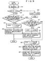
- controller 20 searches directory memory 35 1 (step 101).
- microprocessor 27 checks whether data to be written in the block of disk unit specified by a command exist in cache memory 33 (step 103).
- step 104 the number of entries whose write command receiving bits are set is counted (step 105).
- the count from the replacement counter is stored in RTCAO register 50 in register file 38 (step 106).
- step 107 of Fig. 9 if microprocessor 27 detects cache miss, controller 20 writes the write data from host system 11 directly in disk unit 10 (step 109), and the flow is ended. However, if YES in step 107, disk controller 20 checks if the specified write instruction designation bit in the disk write instruction from host system 11 is set, i.e., if the disk write instruction is the specified write instruction (step 111).
- controller 20 If NO in step 111, controller 20 writes the write data from host system 11 in cache memory 33 and the disk unit 10 (step 113). Controller 20 then updates the replacement counter in the bit entry in directory memory 35 1 (step 115), and the flow is ended.
- controller 20 retrieves the contents of RTCAO 50 to check if there are N or more entries whose write command receiving bits are set, i.e., if there are N or more blocks which have been written in cache memory 33 but not yet in disk unit 10 (step 117).
- controller 20 If NO in step 117, controller 20 writes the write data from host system 11 in cache memory 33, but does not write it in unit 10 (step 119). Controller 20 sets the write command receiving bit in the hit entry in directory memory 35 1 (step 121), and the flow is ended.
- controller 20 3rites the write data from host system 11 in cache memory 33 and disk unit 10 (step 123). Controller 20 writes certain of the blocks not written in disk unit 10 in memory 33, i.e., those which correspond to the directory memory 35 1 entries whose write command receiving bits are set (step 125). In this case, the number of blocks to be written in unit 10 is determined to be smaller than N (e.g., N - 2). The operation in step 125 is performed such that the number of blocks not written in disk unit 10 is smaller than the maximum number N of blocks to be written in disk unit 10 in a back-up operation mode, i.e., at the time of power failure. Controller 20 then resets write command receiving bits of directory memory 35 1 entries corresponding to the cache blocks written in unit 10 (step 127), and the flow is ended.
- the corresponding write data is registered in cache memory 33 but not in disk unit 10, thereby decreasing the write cycles of the disk unit 10.
- the number of blocks written in cache memory 33 but not in unit 10 is controlled to be smaller than N. At the time of power failure, the blocks not written in unit 10 are then written therein (to be described later).
- controller 20 searches directory memory 35 1 (step 129) to check if the data in unit 10 specified by the instruction exists in cache memory 33, i.e., if cache hit is detected (step 131).
- controller 20 If YES in step 131, controller 20 reads out the target data from the cache block in cache memory 33 so as to correspond to the hit entry in directory memory 35 1 . The readout data is sent to host system 11 (step 133). Controller 20 sets or resets the resident bit of hit entry in memory 35 1 according to the content of the resident designation bit of the disk read instruction (step 135), and the flow is ended. The replacement counter area in each hit entry is updated in step 135.
- controller 20 checks if all resident bits of the entries in directory memory 35 1 are set (step 137).
- controller 20 determines that no cache blocks to be replaced exist and transfers the read data from unit 10 to only host system 11 (step 139). In this case, the read data is not written in cache memory 33.
- controller 20 determines the entry to be replaced according to the LRU algorithm (i.e., the content of the replacement counter) (step 141).
- the cache block corresponding to this entry is detected as the cache block to be replaced.
- disk controller 20 checks if the write command receiving bit of the entry to be replaced is set (step 143).
- controller 20 If YES in step 143, controller 20 writes the cache block corresponding to this entry, i.e., the data of cache block to be replaced, in disk unit 10 (step 145). ' Controller 20 then transfers read data from unit 10 (specified by the disk read instruction from host system 11) to system 11 and performs data write in the cache block data to be replaced (step 147). Controller 20 sets a disk block address and the initial value for the replacement counter in the entry (the entry to be replaced) in directory memory 35 1 which specifies the cache block. At the same time, controller 20 resets the write command receiving bit and sets or resets the resident bit according to the content of the resident designation bit of the disk read instruction from host system 11 (step 149).
- the cache block corresponding to the directory memory 35 1 entry whose resident designation bit is set in step 149 is excluded from the blocks subjected to replacement.
- This block data i.e., the data of the disk block specified by the disk read instruction resides in cache memory 33 at least until the resident bit is reset (i.e., until resident cancel of the cache block data) in response to the resident designation bit in the disk read instruction.
- the disk block residence can be specified in response to the resident designation bit of the disk read instruction, or can be performed with software. This operation is used for high-speed jobs, thereby improving overall system performance.
- Power failure is detected by a cutoff detector (not shown).
- a power source used in this embodiment is designed to be operated for a predetermined period of time after the cutoff detector detects a power failure. During this back-up period, disk controller 20 performs the following operation. If the cutoff detector detects a power failure, controller 20 interrupts the currently executed processing (step 151). Controller 20 accesses directory memory 35 1 and sequentially writes cache block data (cache block data not written in disk unit 10) corresponding to the entry whose write command receiving bit is set (step 153).
- the number of cache blocks corresponding to the entries whose write command receiving bits are set is smaller than the maximum number N of blocks to be written in unit 10 during the back-up period after the power failure. Therefore, all block data not written in unit 10 can be properly written therein, in step 153. At the time of system initialization after the power failure, data can be read from unit 10 without read errors. In this embodiment, it is possible to provide most of the non-written blocks as continuous resident blocks in the disk area upon resident designation of the disk write instruction. This indicates that high-speed write of non-written blocks in unit 10 can be performed and the N value can be increased.
- the disk access request from host system 11 is held in command register 21 1 in HDC 21 through D/R 25 and bus 24. This request is read out by microprocessor 27 and stored in a predetermined area of work memory 29. At the same time, microprocessor 27 supplies a seek command to HDC 21. HDC 21 controls disk unit 10 to seek a track specified by the seek command. Microprocessor 27 supplies the disk block number corresponding to the disk unit area subjected to data access and the directory memory address to directory search circuit 35 2 through bus 26, D/R 32, and bus 31. Microprocessor 27 initializes circuit 35 2 . Search circuit 35 2 performs directory search using the disk block number as the target. The directory search result is held in directory memory/ search circuit 35.
- Microprocessor 27 produces at least one cache operation designation data according to the disk block number held in directory memory/search circuit 35 and the contents of the disk access request.
- the produced data is stored in address stack memory 45 through bus 26, D/R 32 and bus 31.
- Data transfer direction control code C in the cache operation designation data represents five modes of operation. These five modes will be described with reference to Figs. 13A through 13E.
- cache memory 33 This is used for cache hit in the disk read request mode. In this case, the contents of cache memory 33 are transferred to host system 11, and disk unit 10 is not accessed, as shown in Fig. 13A.
- disk unit 10 is read-accessed, and the readout data is transferred to host system 11 through buffer memory 30 and, at the same time, is written in cache memory 33.
- cache operation designation data will be described below. Assume that a disk access request from host system 11 represents disk read for 6 sectors starting from sector number 10, and that cache miss occurs during the disk read. Also assume that one track of the disk consists of 64 sectors (sector 0 through sector 63), and that one block of cache memory 33 consists of 64 sectors.
- microprocessor 27 When microprocessor 27 detects the cache miss in read operation according to the directory search result of directory memory/search circuit 35, microprocessor 27 read-accesses the ID field of the disk. The readout data is latched in ID register 21 2 in HDC 21 to read the sector number from the ID field.
- Microprocessor 27 subdivides the updating cache block into subunits by use of cache addresses each corresponding to the sector next to that of the read sector number, the start sector of the disk area subjected to transfer to the host system, and the end sector. Cache operation designation data are prepared for the respective subunits. Assuming that the read sector number is 4, the cache block is subdivided into subunit A corresponding to the disk area of sector numbers 0 through 4, subunit B of sector numbers 5 through 9, subunit C of sector numbers 10 through 15, and subunit D of sector numbers 16 through 63. When data is read from sector number 5, i.e., when data transfer is performed in an order of B, C, D, and A, effective data transfer without awaiting disk rotation can be achieved.
- the cache block shown in Fig. 14 shows one block in cache memory 33.
- the cache block is subdivided into subunits A, B, C, and D. Of course, the cache block is not physically divided into subunits.
- Numeric values 0 to 63 represent the disk sector numbers. Data of disk sector numbers 5 to 9, for example, is written in subunit B starting with address aB.
- Microprocessor 27 first produces cache operation designation data for subunit B and pushes down the data in address stack memory 45 through bus 26, D/R 32, and bus 31.
- Microprocessor 27 then produces cache operation designation data for subunit C and pushes it down in address stack memory 45.
- microprocessor 27 produces cache operation designation data for subunit D and pushes it down in memory 45.
- microprocessor 27 produces cache operation designation data for subunit A and pushes it down in memory 45.
- microprocessor 27 When microprocessor 27 completes production of cache operation designation data and its storage in address stack memory 45, microprocessor 27 sends a control signal to HDC 21 to designate disk read of 59 sectors starting from sector number 5, i.e., the disk read from the start sector of the disk area corresponding to subunit B to the last sector of the corresponding track. Microprocessor 27 sets the start address for address stack memory 45 in stack address counter 46, and starts cache control circuit 34.
- HDC 21 receives the disk read command from microprocessor 27 and data of the specified area from disk unit 10 and stores them in buffer memory 30 through bus 26.
- DMA 21 3 in HDC 21 sends a data transfer request to host system 11 through control line 23, and, at the same time, a data transfer request to cache control circuit 34.
- DMA 21 3 receives the response signals from host system 11 and cache control circuit 34, it reads the data from buffer memory 30 and sends it onto data line 22. This read operation is time-divisionally performed with storage in memory 30.
- circuit 34 When cache control circuit 34 is initialized by microprocessor 27, circuit 34 reads the specified data from the area (corresponding to subunit B of Fig. 14) of memory 45 which is accessed by stack address counter 46. Cache control circuit 34 sends address and write signals to cache memory 33, and sequentially writes data output from DMA 21 3 on line 22 in the specified area of memory 33 in synchronism with data transfer by DMA 213. In this case, cache control circuit 34 controls D/R 25 to inhibit data transfer to host system 11 via line 22.
- cache control circuit 34 When cache control circuit 34 completes data write for subunit B, it controls stack address counter (SAC) 46. In other words, when address aB is updated by address kB, SAC 46 is incremented by one.
- the next cache operation designation data i.e., that for subunit C, is read from address stack memory 45 and designated control is performed. More specifically, the data sequentially sent from DMA 21 3 onto line 22 are sequentially written in subunit C of the cache memory 33. At the same time, D/R 25 is controlled to transfer data from line 22 to system 11.
- cache control circuit 34 performs control specified by the next cache operation-designation data, i.e., the cache operation designation data for subunit D. Control circuit 34 writes data from line 22 in the designated subunit D of cache memory 33 and, at the same time, controls D/R 25 to inhibit write operation of data from line 22 to system 11.
- HDC 21 After HDC 21 completes the write operation for subunits B, C, and D, it detects an index pulse, as shown in Fig. 15, and then interrupts microprocessor 27. Upon detection of the interrupt from HDC 21, microprocessor 27 desigates disk read for subunit A (sector 0 through sector 4). HDC 21 receives data of disk area corresponding to subunit A, and stores it in buffer memory 3 0 . The data buffered in memory 30 is sent by DMA 21 3 in HDC 21 onto line 22, and is written in subunit A of cache memory 33 under the control of cache control circuit 34. In this case, data transfer to system 11 via line 22 is inhibited.
- the disk access request from host system 11 represents cache miss in the disk read of 6 sectors, starting from sector number 10, and the current read sector number is 4.
- a disk access request from host system 11 represents disk read of 6 sectors, starting from sector number 10, and the current read sector number is 12.
- the cache block is subdivided into subunit A corresponding to a disk area of sector numbers 0 through 9, subunit B corresponding to sector numbers 10 through 12, subunit C corresponding to sector numbers 13 through 15, and subunit D corresponding to sector numbers 16 through 63.
- data is read from sector number 13, i.e., if data transfer is performed in an order of C, D, A, and B, effective data transfer without awaiting disk rotation can be achieved.
- Microprocessor 27 first produces cache operation designation data for subunit C and pushes it down in address stack memory 45.
- Microprocessor 27 produces cache designation data for subunit D and pushes it down in address stack memory 45.
- Microprocessor 27 then produces cache operation designation data for subunit A and pushes it down in address stack memory 45.
- microprocessor 27 produces cache operation designation data for subunit B and pushes it down in address stack memory 45.
- Data can be read in an order of subunits C, D, A, and B under the control of cache control circuit 34, as in the embodiment of Fig. 14.
- data transfer control is performed according to the cache operation designation data consisting of the transfer start cache address, the number of transfer sectors, and the data transfer direction control code, data transfer can be effectively performed upon occurrence of a read error caused by storage of data not requested by the host system but written in the cache memory.
- the disk read operation upon occurrence of the cache miss in read operation, since data transfer is started with a read enable sector, disk rotation need not be awaited and high-speed transfer can be performed.
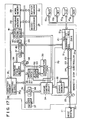
- FIG. 17 An embodiment of a magnetic disk controller for using a cache memory regardless of the number of magnetic disk units will be described below.
- the same reference numerals in the embodiment of Fig. 17 denote the same parts as in the embodiment of Fig. 2, and a detailed description thereof will be omitted.
- magnetic disk units 10 1 through 10 4 are connected to HDC 21.
- Fig. 18 shows a directory data format.
- the directory data is 4-byte data consisting of first to fourth bytes.
- the first byte consists of 3-bit drive number LUN (Logical Unit No.) as a magnetic disk drive identifier, and upper 5 bits (address U) of a 15-bit disk block address.
- the second byte consists of 8 bits (address M) of the disk block address which follow address U.
- the third byte consists of the remaining lower two bits (address L) of the disk block address, 4-bit all "0" data, one-bit error flag ERR, and one-bit valid display flag VB.
- the fourth byte consists of an 8-bit LRU (Least Recently Used) value.
- the directory data is produced on the basis of drive number LUN, the disk logical address, etc., included in the read/write command.
- Fig. 19 shows a read/write command format.
- This command is a 6-byte instruction including a command code for designating the read/write operation, drive number LUN, the disk logical address, the number of data blocks, and cache control bits CC2 through CCO.
- Drive number LUN consists of three bits to access one of disk units 10 1 through 10 4 .
- the MSB of drive number LUN is always logic "0".
- the disk logical address represents a disk sector number designated by drive number LUN, and consists of a 5- bit logical address 2, 8-bit logical address 1, and 8-bit logical address 0, a total of 21 bits.
- one block consists of 16 Kbytes. As shown in Fig.
- bits 6 through 20 of the disk logical address represent a disk block address.
- the capacity of cache memory 33 is 512 Kbytes, and one cache block consists of 16 Kbytes.
- the number of columns is 2, namely: column 0 and column 1.
- Each columns of cache memory 33 includes 16 cache blocks. Therefore, bit 6 of the disk logical address represents the column number.
- Fig. 20 shows a structure of directory memory 35 1 .
- the capacity of memory 35 1 is 128 bytes and consists of the column 0 area (64 bytes) starting with address 000 (hexadecimal), and the column 1 area (64 bytes) starting with address 040 (hexadecimal).
- the areas of columns 0 and 1 are subdivided into 16 areas (hereinafter, each called as to "level") each. Each level consists of 4 bytes.
- the directory data in Fig. 18 can be registered in each level.
- the read/write command (Fig. 19) from host system 11 is retained in command register 21 1 in HDC 21 through D/R 25 and bus 24. This command is read out from register 21 1 under the control of microprocessor 27, and is stored in a predetermined area of work memory 29. In this state, microprocessor 27 issues a seek command which is then set in HDC 21. HDC 21 controls a specified one of magnetic disk units 10 1 through 10 4 so as to seek the designated track.
- Microprocessor 27 checks bit 6 (i.e., the column number) of the disk logical address, and checks if the disk block address including the disk logical address in the read/write command is registered in directory memory 35 1 . If bit 6 is set at logic "0", the column 0 area of directory memory 35 1 serves as the area subjected to directory search. Microprocessor 27 sets "000" (hex) as the directory start address in CDMA 40.
- microprocessor 27 sets "040" (hex) in CDMA 40.
- Microprocessor 27 sets drive number LUN and bits 16 through 20 (logical address 2) of the disk logical address in the read/write command in RTCAO register 50 in register file 38. At the same time, microprocessor 27 sets bits 8 through 15 (logical address 1) of the disk logical address in RTCAl register 51. Microprocessor 27 sets data consisting of bits 6 and 7 of the disk logical address, the 4-bit all "0" data, error flag ERR of logic "0", and valid display flag VB of logic "1" in R TCA2 register 52. Microprocessor 27 sets the LRU value (minimum LRU value) of 0 in RTCA3 register 53. Microprocessor 27 produces target data for directory search on the basis of drive number LUN and the disk logical address in the read/write command, and sets it in register file 38.
- microprocessor 27 causes cache control circuit 34 to perform directory search.
- the following directory search cycle is repeated 16 times.
- the directory memory address specified by CDMA 40 is set in RCGAO register 60 in file 41.
- the directory data of a level represented by CDMA 40 is read out from memory 35 1 from the first byte to the fourth byte onto bus 31.
- the readout byte data is supplied to the B input of comparator 39.
- the target data is read out from file 38 from the first byte in units of bytes.
- the readout target data is supplied to the A input of comparator 39.
- Comparator 39 compares the contents of the A and B inputs. The comparison result is supplied from comparator 39 to cache control circuit 34.
- the LRU value in the directory data supplied from directory memory 35 to the B input of comparator 39 through bus 31 is then loaded in CLRU 36 and incremented by one.
- Cache control circuit 34 determines if cache hit occurs according to the comparison results for the first through third bytes in comparator 39. If cache hit is detected, control circuit 34 adds a cache hit flag to the directory memory address set in RCGAO register 60 in file 41, i.e., in the address representing the start position of the corresponding level of the current directory search cycle. The address with the cache hit flag is then set in RCGA1 register 61.
- Cache control circuit 34 determines the level of memory 35 which corresponds to the candidacy of the cache block to be replaced at this time, according to the LRU value comparison result of comparator 39. If the LRU value from directory memory 35 exceeds that from register file 38, control circuit 34 determines that the cache block corresponding to the level is a cache block to be replaced. In this case, control circuit 34 transfers the directory memory address from RCGAO register 60 in file 41 to RCGA2 register 62. Control circuit 34 causes driver 37 to send the unitary incremented LRU value specified by CLRU 36 onto bus 31, and updates the LRU value set in register 53 in file 38 to the LRU value on bus 31.
- Cache control circuit 34 writes the LRU value of CLRU 36 on bus 31 in the corresponding level of directory memory 35, regardless of the comparison result of comparator 39.
- the LRU value in the corresponding level in directory memory 35 is incremented by one for every directory search cycle.
- the above operation is the directory search cycle.
- the cycle is repeated for the respective directory data of levels 0 through F (hexadecimal) in directory memory 35, thereby completing directory search corresponding to the read/write command.
- cache hit is detected and the start address of the level corresponding to the cache block is set in RCGA1 register 61 in file 41.
- the start address of the level having the largest LRU value in the specified column is stored in RCGA2- register 62 in file 41. This address represents the directory memory 35 level corresponding to the cache block to be replaced if cache miss occurs in the read mode.
- microprocessor 27 fetches the content of RCGA1 register 61 in file 41 through bus 26, and checks the flag mentioned above if cache hit or miss occurs. If cache miss occurs in the read mode, microprocessor 27 writes the directory address of RCGA2 register 62 in file 41 as the oldest cache block at this time, i.e., the start address of the directory memory 35 level corresponding to the cache block to be replaced. This start address is set in CD MA 40. Microprocessor 27 registers the directory data in the level corresponding to directory memory 35 while the contents of CDMA 40 are sequentially counted. The directory data is substantially the same as the target data in register file 38, except that the LRU value is the initial value. In this embodiment, the initial value of the LRU value is specified by cache control bits CC2 through CCO.
- the block of the cache memory 33 to be replaced for a disk block in the disk units of this embodiment can be determined according to the magnitudes of the LRU values of the directory data for each level in the same manner as in the magnetic disk controller for controlling the single magnetic disk unit. Therefore, unlike the conventional system, the area of directory memory 35 can be assigned to any one of units 10 1 through 10 4 , as shown in Fig. 21. Thus, in this embodiment, cache memory 33 can be effectively utilized according to the access frequency of units 10 1 through 1 0 4 .
- cache memory 33 is commonly used by magnetic disk units 10 1 through 10 4 .
- the cache memory need not be used.
- the cache memory is commonly used by other, remaining drive units.
- cache memory 33 having a limited capacity, can be effectively used, and the hit rate can be increased. Whether the cache memory is used is determined by a command at the time of system initialization in units of magnetic disk drive units.
- the above embodiments exemplify the disk cache system for a magnetic disk.
- the present invention can also be applied to disk cache systems such as floppy disk drive units, optical disk systems or RAM disk units.
Abstract
Description
- The present invention relates to a cache system adopting an LRU (Least Recently Used) system in a replacement algorithm for cache blocks, and to a magnetic disk controller incorporating the cache system.
- Disk cache systems capable of high-speed data access to magnetic disks have been developed. A disk cache is a memory device using a semiconductor RAM and is designed to eliminate an access gap between a high-speed main memory and low-speed large-capacity secondary memories (i.e., magnetic disk units). The disk cache is normally arranged between the main memory and a magnetic disk unit, in a magnetic disk controller, and serves as a data buffer.
- The principle of the disk cache is the same as that of a central processing unit (CPU) cache. If a CPU first accesses part of a file, necessary data blocks are stored on a disk. In this case, the disk cache does not contribute to such CPU access.
- Necessary blocks are transferred from the disk to the main memory. At the same time, they are written in the disk cache. If the CPU subsequently accesses the same blocks, they are transferred from the disk cache, but not from the disk. The access time of the magnetic disk unit is normally 20 to 30 ms, while the access time of the disk cache is about 1 to 3 ms. The access time can, therefore, be decreased to about 1/10. When a total access time is regarded as an input/output response time including data transfer time and channel wait time, it can be normally decreased to 1/2 to 1/3.
- Since a disk cache capacity is smaller (about 1/1000) than that of the disk, all file blocks required by the CPU are not always stored in the disk cache. In order to load new blocks when the disk cache is filled with file blocks, old blocks must be removed from it. When accessing of the cache allows retrieval of necessary data from the cache, it is called a "hit", and when retrieval of necessary data cannot be performed, it is called a "miss". The average hit times per times of the difference of the cache is called a hit ratio.
- In addition to the disk cache, disk cache mechanism components are a disk cache handler as a program in the input/output controller, a data transfer mechanism between the main memory and the disk cache, and a disk cache directory. The disk cache handler cooperates with an operating system (OS) to determine the hit/miss ratio of the disk cache, control of data transfer between the main memory, the disk cache, and the magnetic disks, and acquisition of data representing utilization efficiency of the disk cache and the hit ratio, and so on.
- Write access schemes include a write through scheme and a write back scheme. The write through scheme is called a store through scheme for writing data directory in a disk. The cache hit processing is performed in such a way that the cache hit block is disabled by not writing data therein, or the data is written in the cache hit block after it is directly written into the disk.
- The write back scheme is called a store in, copy back, or post store scheme. According to this scheme, the disk cache write is the highest priority. When data write into a file in the disk cache is completed, data input/output is completed. If the file is unnecessary or the cache block storing the file must be emptied for other files, data is transferred from the cache to the disk.
- In the disk cache, data copying from the magnetic disk to the cache memory is called staging, and copying from the cache memory to the magnetic disk is called destaging.
- A typical disk cache memory mapping scheme is a set associative scheme. According to this scheme, the magnetic disk and the disk cache memory are divided into a plurality of blocks (e.g., one block = one track = 64 sectors). Each block belongs to any one of columns. In order to transfer a given block from the magnetic disk to the cache memory, this block is written in an identical column of the cache memory and data (representing which block, i.e., a block number, in the magnetic disk is stored in the cache memory) is stored in the directory in units of columns. By referring this directory, it is possible to determine whether specific data is stored in the cache memory or not. If the data is stored in the cache memory, it can be read out, not from the magnetic disk unit but from the cache memory.
- The disk cache replacement algorithm is an LRU algorithm. LRU stands for "Least Recently Used." According to the LRU algorithm, the block which stays in the cache for the longest period after the last access is selected as the least necessary block. In a disk cache having no empty space, if the cache memory must be assigned for new staging, the least necessary track data is removed to obtain an empty space. The LRU algorithm is used to assure this empty space.
- If a cache hit occurs as a result of the directory search, the LRU value in the cache directory corresponding to the hit cache block is initialized to "0". In the case of cache miss, the LRU value corresponding to the cache block to be replaced must be registered again. In this case, if the cache miss occurs in the read request mode, the corresponding data block is read out from the magnetic disk unit and is stored in the cache block in the cache memory which is to be replaced.
- In a conventional cache system, LRU setting values are determined regardless of the data blocks stored in the cache memory.
- The frequency of use of the data blocks stored in the cache blocks varies according to different types of files. Once a data block having a low frequency of use is stored in -the cache block, the resident possibility of that data block in the cache memory is often higher than that of a file having a high frequency of use. Because of this, a decrease in hit rate of the cache memory tends to occur.
- In the conventional disk cache system of this type, disk write operation is always performed in response to a disk write instruction from a host system. According to the conventional system, even if the data in the disk area subjected to disk write is stored in the cache memory (even if cache hit occurs), the contents of the cache memory and the disk unit are simultaneously updated. This is not to allow non-updated data to be left in the disk when a failure, such as a power failure, occurs.
- According to the system described above, however, high performance of the disk cache structure can be achieved only when a read frequency is high. If the write frequency is high, a great deal of improvement in performance cannot be expected.
- When a power unit free from the effects of power failure is used, disk write need not be performed at the time of cache hit in the write request mode. However, a power unit of this type is very expensive.
- Assume that a read access request for a given file is sent from the CPU. The magnetic disk controller retrieves a disk cache directory (a table having file information such as a file name, a file size, and a file address) and checks if the data block of interest is stored in the disk cache. If cache hit occurs, the corresponding data block is transferred from the cache memory to the main memory.
- In the case of cache miss, however, several blocxs (usually those for one track) including the required block are sent to the cache memory, and only the required block is sent to the main memory. Data transfer to the cache memory is performed simultaneously witn that to the main memory. However, the blocks can be transferred to the cache memory and the block of interest can be transferred to the main memory thereafter.
- A large demand has arisen for a magnetic disk controller for satisfying the above-mentioned two transfer schemes and for performing effective data transfer control if cache miss occurs.
- If a cache memory is commonly used by, e.g., 4 magnetic disk drives DKO through DK3, different cache memory areas are permanently assigned for respective drives DKO through DK3, and a directory memory having a corresponding memory allocation is prepared, as shown in Fig. 1.
- According to the system described above, however, the limited area of the cache memory is divided, and the cache locations respectively assigned to the magnetic disk drives are decreased, leading to a reduction in the cache hit rate. If the access frequency varies for the different drives, the frequency of use of the cache memory location corresponding to the drive having the lowest access frequency is decreased. As a result, the overall utilization efficiency of the cache memory is degraded.
- It is an object of the present invention to provide a cache system wherein setting values for LRU initialization or re-registration are variables and the resident possibility of data blocks in the cache memory can be controlled.
- It is another object of the present invention to provide a disk cache system wherein the frequency of data written in the disk can be decreased without using an expensive power source unit to improve system performance.
- It is still another object of the present invention to provide a magnetic disk controller for effectively performing data transfer control upon occurrence of read errors and for achieving high-speed transfer.
- It is still another object of the present invention to provide a magnetic disk controller capable of effectively using a cache memory in common for a plurality of magnetic disk drives, regardless of their number.
- In order to achieve the above objects of the present invention, there is provided a cache system employing an LRU (Least Recently Used) scheme in a replacement algorithm of cache blocks, comprising:
- a cache memory for storing a plurality of cache blocks;
- a directory memory having fields storing, in respective entries corresponding to respective cache blocks of said cache memory, designation data for blocks registered in said cache memory and LRU counter fields indicating resident status in said cache memory of these blocks;
- command issuing means for issuing a read/write command to which an arbitrary LRU setting value and designation data for a read/write target block are appended;
- directory search means for searching whether the read/write object block is registered in said cache memory by comparing the registered block designation data of respective entries with the read/write designation data; and
- registering means for registering the arbitrary setting value appended to the read/write command in a hit entry of said directory memory when hit occurs, and in the LRU counter field of an entry corresponding to the cache block in which the read/write target block is registered when a miss hit occurs.
- This invention can be more fully understood from the following detailed description when taken in conjunction with the accompanying drawings, in which:
- Other objects and features of the present invention will be apparent from the following description taken in connection with the accompanying drawings, in which:
- Fig. 1 is a schematic view showing the correspondence between a cache memory and a directory memory in a conventional system;
- Fig. 2 is a block diagram showing an embodiment of a magnetic disk controller incorporating a disk cache memory according to the present invention;
- Fig. 3 is a format showing an entry structure of a directory memory in Fig. 2;
- Fig. 4 is a format of a read/write command used in the system of Fig. 2;
- Fig. 5 is a format of an LRU setting value;
- Fig. 6 is a format of directory data stored in
directory memory 351 according to another embodiment of a disk cache system of the present invention; - Fig. 7 is a format showing the main part of a disk write instruction employed in the embodiment of Fig. 6;
- Fig. 8 is a format showing the main part of a disk read instruction used in the embodiment of Fig. 6;
- Figs. 9 through 12 are flow charts for explaining the operation of the embodiment in Fig. 6, in which Fig. 9 is a flow chart for explaining control of
magnetic disk controller 20 when the disk write instruction is supplied thereto from a host system, Fig. 10 is a flow chart of the search subroutine, Fig. 11 is a flow chart for explaining control ofmagnetic disk controller 20 when the disk read instruction is supplied thereto from the host system, and Fig. 12 is a flow chart for explaining the operation ofmagnetic disk controller 20 during a power failure; - Figs. 13A through 13E are views for explaining the operation contents of data transfer direction control code C used in the magnetic disk controller according to the present invention;
- Fig. 14 is a chart for explaining cache operation designation data produced upon occurrence of a read error;
- Fig. 15 is a timing chart for explaining the disk read operation in Fig. 14;
- Fig. 16 is a chart for explaining another cache operation designation data;
- Fig. 17 is a block diagram showing another embodiment of a magnetic disk controller according to the present invention;
- Fig. 18 is a format of directory data used in the embodiment of Fig. 17;
- Fig. 19 is a format of a read/write command used in the embodiment of Fig. 17;
- Fig. 20 is a data format of a directory memory used in the embodiment of Fig. 17; and
- Fig. 21 is a schematic view showing the correspondence between
cache memory 33 anddirectory memory 351 in the embodiment of Fig. 17. - Fig. 2 is a block diagram showing an embodiment of
magnetic disk controller 20 incorporating a disk cache system. Hard disk control circuit (to be referred to as an HDC hereinafter) 21 for controllingdisk unit 10 is connected to hostsystem 11 throughfirst bus 24, which consists ofdata line 22 andcontrol line 23, and driver/receiver (to be referred to as a D/R hereinafter) 25.HDC 21 is also connected tosecond bus 26.HDC 21 consists ofcommand register 211,ID register 212, andDMA 213.Bus 26 is also connected tomicroprocessor 27 for controlling the overall operation ofcontroller 20,program memory 28 storing control programs (microprograms) formicroprocessor 27,work memory 29 used as a work area ofmicroprocessor 27, andbuffer memory 30 for compensating a difference between the transfer rates ofdisk unit 10 andhost system 11.Third bus 31 is connected tocache control circuit 34, mainly for controlling data transfer, the operation of which includes control ofcache memory 33, directory memory/search circuit 35 consisting ofdirectory memory 351 anddirectory search circuit 352, and addressstack memory 45.Memory 45 is a FIFO (first-in first-out) stack for storing cache operation designation data consisting of three parameters. These three parameters are transfer start cache address a, the number of transfer sectors Q, and data transfer direction control code C. The output of stack address counter 46 is connected to address port A ofaddress stack memory 45.Bus 26 is connected to the input of counter 46. -
Bus 31 is connected to the input to LRU counter (referred to as an CLRU hereinafter) 36 for storing an LRU value read out frommemory 351 in the directory search mode, as well as the output ofdriver 37. The output ofCLRU 36 and the input ofdriver 37 are connected tocache control circuit 34.Bus 31 is also connected to the input port ofregister file 38 and the B input ofcomparator 39. The A input ofcomparator 39 receives the data frombus 31. The output port ofcomparator 39 is connected to controlcircuit 34.Control circuit 34 is connected to registerfile 38 to control inputs thereto, i.e., theCLRU 36 contents (LRU values) output bydriver 37 onbus 31.File 38 comprises fourregisters 50 through 53, i.e., RTCAO through RTCA3. - The output of directory memory address counter (to be referred to as a CDMA hereinafter) 40 is connected to address port A of
directory memory 351 to designate the addresses ofmemory 351. The input ofCDMA 40 is connected tosecond bus 26. The output ofCDMA 40 is connected to the input ofregister file 41. The output offile 41 is also connected tobus 26.File 41 is connected throughcontrol line 65 so as to receive control signals fromcache control circuit 34.Register file 41 consists of threeregisters 60 through 62, i.e., RCGAO through RCGA2. - Each entry of
directory memory 351 includes disk block number field (8 bits) 81 representing the number of data blocks registered incache memory 33, and LRU counter field (8 bits) 83 representing an LRU value, as shown in Fig. 3. The number of entries inmemory 351 is equal to that of cache blocks incache memory 33. In this embodiment, 16 entries are given for each column. One track ofdisk unit 10 consists of 64 sectors, each corresponding to one block ofcache memory 33. The area ofdisk unit 10 is divided intocolumn 0 andcolumn 1 which store data in units of 64 sectors. A column value is represented by the seventh bit from the LSB of a disk logical address (to be described later). The disk block number is represented by the MSB excluding the lower seven bits of the disk logical address. - The magnetic disk controller of this embodiment has the following features:
- (i) One sector of the magnetic disk consists of 256 bytes.
- (ii) One block (cache block) of
cache memory 33 consists of 16K bytes (64 sectors) and therefore one block (disk block) of the disk consists of 16K bytes (64 sectors). - (iii) A mapping scheme of
cache memory 33 is a set associative scheme. - (iv) A cache block replacement scheme is an LRU scheme.
- (v) The number of levels (i.e., the number of entries) of
directory memory 351 is 16 per column. - (vi) The capacity of
cache memory 33 is 512 Kbytes. - The operation of the embodiment shown in Fig. 2 will be described below.
- A read/write command from
host'system 11 is stored incommand register 211 inHDC 21 through D/R 25 andbus 24. The read/write command is a 6-byte instruction includingcommand code 85 for designating read/write operation or the like, a disk logical address consisting of logical address 2 (MSB) 87,logical address 1 89, and logical address 0 (LSB) 91, the number of data blocks, and each field 93 of cache control bits CC2 through CCO (Fig. 4). - The read/write command in
register 211 is read out bymicroprocessor 27 and stored in a predetermined area ofwork memory 29. Whenmicroprocessor 27 stores the read/write command fromhost system 11 inmemory 29,microprocessor 27 issues a seek command which is then set incommand register 211 inHDC 21.HDC 21controls disk unit 10 to seek a specified track.Microprocessor 27 also sets, in accordance with the read/write command, a disk block number corresponding to the access area ofdisk unit 10, and an LRU value of "0" inregister file 38 throughbus 26, D/R 32, andbus 31.Microprocessor 27 sets bit 6 of logical address 0 (Fig. 4), i.e., the start address of the currently read-accessed entry in each area (for 16 entries) indirectory memory 35jr inCDMA 40. In this case, each area is accessed by the column value. The following directory search cycle is repeated 16 times. - In the directory search cycle, the address specified by
CDMA 40 is set inRCGAO 60 inregister file 41. Therefore, the start position of the entry currently searched is always stored inRCGAO 60 inregister file 41. -
CDMA 40 is sequentially counted up. Directory data of the entry indirectory memory 351 is read out ontobus 31 in units of bytes in response to the count from theCDMA 40. The readout directory data is supplied to the B input ofcomparator 39. Byte data fromregister file 38 is supplied to the A input ofcomparator 39 in response to the data supplied to the B input.Comparator 39 compares the contents of the A and B inputs. - The comparison result of
comparator 39, i.e., the result of comparison of the target data block number fromfile 38 with the registered data block number frommemory 351 in units of bytes, is supplied tocache control circuit 34. The result of comparison between the LRU value fromfile 38 and that frommemory 351 is also supplied tocache control circuit 34. The LRU value supplied frommemory 351 to the B input ofcomparator 39 throughbus 31 is supplied to CLRU 36. The LRU value stored inCLRU 36 is incremented by one. -
Cache control circuit 34 determines if cache hit occurs according to the data block number comparison result fromcomparator 39. Ifcircuit 34 determines that coincidence is detected bycomparator 39 and cache hit occurs, it appends a cache hit flag to the address set inRCGAO 60 inregister file 41, i.e., to the address representing the start position of the entry being searched in the current directory search cycle. The address with a cache hit flag is set inRCGAl 61 inregister file 41.Cache control circuit 34 determines the entry ofdirectory memory 351 which corresponds to the cache block to be replaced at this time, according to the LRU value comparison result. More specifically, if the LRU value frommemory 351 exceeds that stored infile 38,cache control circuit 34 determines that the cache block corresponding to the entry is a candidacy of block to be replaced.Control circuit 34 transfers the address from RCGAO 60 infile 41 to RCGA2 62 therein.Control circuit 34 causesdriver 37 to send the incremented LRU value fromCLRU 36 ontobus 31. The LRU value inregister file 38 is then updated to correspond with that appearing onbus 31.Cache control circuit 34 also writes the LRU value stored inCLRU 36 viabus 31 in the corresponding entry indirectory memory 351, regardless of the comparison result ofcomparator 39. In this embodiment, the LRU value in the corresponding entry inmemory 351 is incremented by one for each directory search cycle. - The above operation is the directory search cycle. This cycle is repeated 16 times to complete the directory search corresponding to the given read/write command. In this case, if cache hit is detected, the start address of the entry in
memory 351 which corresponds to the hit cache block is set inRCGAl 61 inregister file 41. The start address of the entry inmemory 351 which has the largest LRU value in the specified column is stored inRCGA2 62. - When the directory search is completed,
microprocessor 27 fetches the content of RCGA1 61 infile 41 throughbus 26, and checks the flag mentioned above in RCG A1 61 whether cache hit or miss occurs. Ifmicroprocessor 27 detects cache hit, the LRU value in the entry inmemory 351 which is specified by the content (directory address) ofRCGA1 61 infile 41 is initialized (or re-registered). However, if the read mode is specified, even if cache miss is detected, the LRU value in the entry inmemory 351 which is specified by the content of RCGA2 62 infile 41 is initialized (or re-registered). In initialization (or re-registration) of the LRU value,microprocessor 27 retrieves the read/write command sent fromhost system 11 and retained inbuffer memory 30.Microprocessor 27 checks if cache control bit CC2 among bits CC2 through CCO is "0". If CC2 = "0", then CC1 and CC2 are defined as LRU setting data. In this case, CC1 and CC2 are shifted to the left by 6 bits to prepare an LRU setting value "CC1 (MSB), CCO, 0, 0, 0, 0, 0, 0 (LSB)", as shown in Fig. 5. The same LRU setting value is supplied todirectory memory 351 throughbus 26, D/R 32, andbus 31, and is registered inLRU counter field 83 of the entry inmemory 351. In LRU value comparison and setting performed byCLRU 36 in the next directory search, the updated LRU setting value is used. If CC1 and CCO are set to be "I", the resident period of the data block incache memory 33 can be decreased. However, if CC1 and CCO are set to be "0", the period can be increased. - Figs. 6 through 12 show another embodiment of a disk cache system wherein the number of write cycles for the disk can be decreased without using an expensive power source, thereby improving system performance.
- Fig. 6 shows a format of directory data stored in
directory memory 351. - Directory data set in each entry in
directory memory 351 consists of a cache active bit representing whether the content of a block (cache block) incache memory 33 for a corresponding entry is effective or not, a write command receiving bit representing whether the write data specified byhost system 11 is completely written indisk unit 10 or not, a resident bit representing whether replacement of the cache block corresponding to this entry is inhibited, a disk address (disk block address) of a data block (disk block) stored incache memory 33, and a replacement counter (replacement counter value) used for replacement operation. - Fig. 7 shows a format of a disk write instruction sent from
host system 11 todisk controller 20. The write instruction includes a specified write instruction designation bit for determining whether the write instruction is the specified write instruction which allows data write incache memory 33 but does not require data write indisk unit 10 when cache hit is detected in the disk write request mode. - Fig. 8 shows a format of a disk read instruction sent from
host system 11 todisk controller 20. The read instruction includes a resident designation bit for designating setting/resetting of a resident bit of an entry (called the replacement entry) inmemory 351 which corresponds to the cache block (subjected to replacement) incache memory 33 when cache miss is detected in the disk read request mode. - The operation of the system described above will be described below. The operation is exemplified by a case with reference to the flow chart of Fig. 9 wherein a disk write instruction is sent from
host system 11 todisk controller 20. - When the disk write instruction is sent from
host system 11 todisk controller 20,controller 20 searches directory memory 351 (step 101). In the search step, as shown in Fig. 10,microprocessor 27 checks whether data to be written in the block of disk unit specified by a command exist in cache memory 33 (step 103). In the case of a write command (step 104), the number of entries whose write command receiving bits are set is counted (step 105). The count from the replacement counter is stored inRTCAO register 50 in register file 38 (step 106). - In
step 107 of Fig. 9, ifmicroprocessor 27 detects cache miss,controller 20 writes the write data fromhost system 11 directly in disk unit 10 (step 109), and the flow is ended. However, if YES instep 107,disk controller 20 checks if the specified write instruction designation bit in the disk write instruction fromhost system 11 is set, i.e., if the disk write instruction is the specified write instruction (step 111). - If NO in
step 111,controller 20 writes the write data fromhost system 11 incache memory 33 and the disk unit 10 (step 113).Controller 20 then updates the replacement counter in the bit entry in directory memory 351 (step 115), and the flow is ended. - However, if YES in
step 111,controller 20 retrieves the contents of RTCAO 50 to check if there are N or more entries whose write command receiving bits are set, i.e., if there are N or more blocks which have been written incache memory 33 but not yet in disk unit 10 (step 117). - If NO in
step 117,controller 20 writes the write data fromhost system 11 incache memory 33, but does not write it in unit 10 (step 119).Controller 20 sets the write command receiving bit in the hit entry in directory memory 351 (step 121), and the flow is ended. - However, if the number of blocks whose data are not written in
unit 10 is N or more,controller 20 3rites the write data fromhost system 11 incache memory 33 and disk unit 10 (step 123).Controller 20 writes certain of the blocks not written indisk unit 10 inmemory 33, i.e., those which correspond to thedirectory memory 351 entries whose write command receiving bits are set (step 125). In this case, the number of blocks to be written inunit 10 is determined to be smaller than N (e.g., N - 2). The operation instep 125 is performed such that the number of blocks not written indisk unit 10 is smaller than the maximum number N of blocks to be written indisk unit 10 in a back-up operation mode, i.e., at the time of power failure.Controller 20 then resets write command receiving bits ofdirectory memory 351 entries corresponding to the cache blocks written in unit 10 (step 127), and the flow is ended. - In the embodiment as described above, if the cache hit is detected in the case of the disk write instruction whose specified write instruction designation bit is set, the corresponding write data is registered in
cache memory 33 but not indisk unit 10, thereby decreasing the write cycles of thedisk unit 10. The number of blocks written incache memory 33 but not inunit 10 is controlled to be smaller than N. At the time of power failure, the blocks not written inunit 10 are then written therein (to be described later). - An operation will be described with reference to the flow chart in Fig. 11, wherein a disk read instruction is sent from
host system 11 todisk controller 20. - When the disk read instruction is sent from
system 11 tocontroller 20,controller 20 searches directory memory 351 (step 129) to check if the data inunit 10 specified by the instruction exists incache memory 33, i.e., if cache hit is detected (step 131). - If YES in
step 131,controller 20 reads out the target data from the cache block incache memory 33 so as to correspond to the hit entry indirectory memory 351. The readout data is sent to host system 11 (step 133).Controller 20 sets or resets the resident bit of hit entry inmemory 351 according to the content of the resident designation bit of the disk read instruction (step 135), and the flow is ended. The replacement counter area in each hit entry is updated instep 135. - However, if NO in
step 131,controller 20 checks if all resident bits of the entries indirectory memory 351 are set (step 137). - If YES in
step 137,controller 20 determines that no cache blocks to be replaced exist and transfers the read data fromunit 10 to only host system 11 (step 139). In this case, the read data is not written incache memory 33. - However, if there is even one directory memory entry whose resident bit is not set,
controller 20 determines the entry to be replaced according to the LRU algorithm (i.e., the content of the replacement counter) (step 141). The cache block corresponding to this entry is detected as the cache block to be replaced. Subsequently,disk controller 20 checks if the write command receiving bit of the entry to be replaced is set (step 143). - If YES in
step 143,controller 20 writes the cache block corresponding to this entry, i.e., the data of cache block to be replaced, in disk unit 10 (step 145).'Controller 20 then transfers read data from unit 10 (specified by the disk read instruction from host system 11) tosystem 11 and performs data write in the cache block data to be replaced (step 147).Controller 20 sets a disk block address and the initial value for the replacement counter in the entry (the entry to be replaced) indirectory memory 351 which specifies the cache block. At the same time,controller 20 resets the write command receiving bit and sets or resets the resident bit according to the content of the resident designation bit of the disk read instruction from host system 11 (step 149). - The cache block corresponding to the
directory memory 351 entry whose resident designation bit is set instep 149 is excluded from the blocks subjected to replacement. This block data, i.e., the data of the disk block specified by the disk read instruction resides incache memory 33 at least until the resident bit is reset (i.e., until resident cancel of the cache block data) in response to the resident designation bit in the disk read instruction. The disk block residence can be specified in response to the resident designation bit of the disk read instruction, or can be performed with software. This operation is used for high-speed jobs, thereby improving overall system performance. - An operation at the time of power failure will be described with reference to the flow chart in Fig. 12.
- Power failure is detected by a cutoff detector (not shown). A power source used in this embodiment is designed to be operated for a predetermined period of time after the cutoff detector detects a power failure. During this back-up period,
disk controller 20 performs the following operation. If the cutoff detector detects a power failure,controller 20 interrupts the currently executed processing (step 151).Controller 20 accessesdirectory memory 351 and sequentially writes cache block data (cache block data not written in disk unit 10) corresponding to the entry whose write command receiving bit is set (step 153). - In this embodiment, the number of cache blocks corresponding to the entries whose write command receiving bits are set is smaller than the maximum number N of blocks to be written in
unit 10 during the back-up period after the power failure. Therefore, all block data not written inunit 10 can be properly written therein, instep 153. At the time of system initialization after the power failure, data can be read fromunit 10 without read errors. In this embodiment, it is possible to provide most of the non-written blocks as continuous resident blocks in the disk area upon resident designation of the disk write instruction. This indicates that high-speed write of non-written blocks inunit 10 can be performed and the N value can be increased. - Still another embodiment for effectively performing data transfer control in the case of read errors will be described with reference to Fig. 2 and Figs. 13A through 15.
- The disk access request from
host system 11 is held incommand register 211 inHDC 21 through D/R 25 andbus 24. This request is read out bymicroprocessor 27 and stored in a predetermined area ofwork memory 29. At the same time,microprocessor 27 supplies a seek command toHDC 21.HDC 21controls disk unit 10 to seek a track specified by the seek command.Microprocessor 27 supplies the disk block number corresponding to the disk unit area subjected to data access and the directory memory address todirectory search circuit 352 throughbus 26, D/R 32, andbus 31.Microprocessor 27 initializescircuit 352.Search circuit 352 performs directory search using the disk block number as the target. The directory search result is held in directory memory/search circuit 35. -
Microprocessor 27 produces at least one cache operation designation data according to the disk block number held in directory memory/search circuit 35 and the contents of the disk access request. The produced data is stored inaddress stack memory 45 throughbus 26, D/R 32 andbus 31. - Data transfer direction control code C in the cache operation designation data represents five modes of operation. These five modes will be described with reference to Figs. 13A through 13E.
- This is used for cache hit in the disk read request mode. In this case, the contents of
cache memory 33 are transferred tohost system 11, anddisk unit 10 is not accessed, as shown in Fig. 13A. - This is used for cache miss in the disk read request mode. As shown in Fig. 13B,
disk unit 10 is read-accessed, and the readout data is transferred tohost system 11 throughbuffer memory 30 and, at the same time, is written incache memory 33. - This is used for cache miss in the disk read request mode and a sector is not requested by the host system but exists in the cache block (undesired sectors may often be written since a write operation is performed in units of blocks). As shown in Fig. 13C, the read data is written in
cache memory 33 but is not transferred to hostsystem 11. - This is used for cache hit in the disk write request mode. As shown in Fig. 13D, the write data from
host system 11 is transferred todisk unit 10 throughbuffer memory 30 and, at the same time, is written incache memory 33. - This is used for cache miss in the disk write request mode. The data from
host system 11 is written inonly disk unit 10 throughbuffer memory 30, but not incache memory 33. - The production of cache operation designation data will be described below. Assume that a disk access request from
host system 11 represents disk read for 6 sectors starting fromsector number 10, and that cache miss occurs during the disk read. Also assume that one track of the disk consists of 64 sectors (sector 0 through sector 63), and that one block ofcache memory 33 consists of 64 sectors. - When
microprocessor 27 detects the cache miss in read operation according to the directory search result of directory memory/search circuit 35,microprocessor 27 read-accesses the ID field of the disk. The readout data is latched inID register 212 inHDC 21 to read the sector number from the ID field. -
Microprocessor 27 subdivides the updating cache block into subunits by use of cache addresses each corresponding to the sector next to that of the read sector number, the start sector of the disk area subjected to transfer to the host system, and the end sector. Cache operation designation data are prepared for the respective subunits. Assuming that the read sector number is 4, the cache block is subdivided into subunit A corresponding to the disk area ofsector numbers 0 through 4, subunit B ofsector numbers 5 through 9, subunit C ofsector numbers 10 through 15, and subunit D ofsector numbers 16 through 63. When data is read fromsector number 5, i.e., when data transfer is performed in an order of B, C, D, and A, effective data transfer without awaiting disk rotation can be achieved. - The cache block shown in Fig. 14 shows one block in
cache memory 33. The cache block is subdivided into subunits A, B, C, and D. Of course, the cache block is not physically divided into subunits.Numeric values 0 to 63 represent the disk sector numbers. Data ofdisk sector numbers 5 to 9, for example, is written in subunit B starting with address aB. -
Microprocessor 27 first produces cache operation designation data for subunit B and pushes down the data inaddress stack memory 45 throughbus 26, D/R 32, andbus 31. As shown in Fig. 14, the cache operation designation data for subunit B consists of transfer start cache address aB for subunit B, the number LB of transfer sectors, and the data transfer direction control code (C = 3). -
Microprocessor 27 then produces cache operation designation data for subunit C and pushes it down inaddress stack memory 45. The cache operation designation data for subunit C consists of transfer start cache address aC, the number iC of transfer sectors, and the data transfer direction control code (C = 2), as shown in Fig. 14. - Subsequently,
microprocessor 27 produces cache operation designation data for subunit D and pushes it down inmemory 45. The cache operation designation data for subunit D consists of transfer start cache address aD, the number iD of transfer sectors, and the data transfer direction control code (C = 3), as shown in Fig. 14. - Finally,
microprocessor 27 produces cache operation designation data for subunit A and pushes it down inmemory 45. The cache operation designation data for subunit A consists of transfer start cache address aA, the number ℓA of transfer sectors, and the data transfer direction control code (C = 3), as shown in Fig. 14. - When
microprocessor 27 completes production of cache operation designation data and its storage inaddress stack memory 45,microprocessor 27 sends a control signal toHDC 21 to designate disk read of 59 sectors starting fromsector number 5, i.e., the disk read from the start sector of the disk area corresponding to subunit B to the last sector of the corresponding track.Microprocessor 27 sets the start address foraddress stack memory 45 in stack address counter 46, and startscache control circuit 34. -
HDC 21 receives the disk read command frommicroprocessor 27 and data of the specified area fromdisk unit 10 and stores them inbuffer memory 30 throughbus 26. When disk read data of one or more sectors is buffered inmemory 30,DMA 213 inHDC 21 sends a data transfer request tohost system 11 throughcontrol line 23, and, at the same time, a data transfer request tocache control circuit 34. WhenDMA 213 receives the response signals fromhost system 11 andcache control circuit 34, it reads the data frombuffer memory 30 and sends it ontodata line 22. This read operation is time-divisionally performed with storage inmemory 30. - When
cache control circuit 34 is initialized bymicroprocessor 27,circuit 34 reads the specified data from the area (corresponding to subunit B of Fig. 14) ofmemory 45 which is accessed by stack address counter 46.Cache control circuit 34 sends address and write signals tocache memory 33, and sequentially writes data output fromDMA 213 online 22 in the specified area ofmemory 33 in synchronism with data transfer byDMA 213. In this case,cache control circuit 34 controls D/R 25 to inhibit data transfer to hostsystem 11 vialine 22. - When
cache control circuit 34 completes data write for subunit B, it controls stack address counter (SAC) 46. In other words, when address aB is updated by address kB, SAC 46 is incremented by one. The next cache operation designation data, i.e., that for subunit C, is read fromaddress stack memory 45 and designated control is performed. More specifically, the data sequentially sent fromDMA 213 ontoline 22 are sequentially written in subunit C of thecache memory 33. At the same time, D/R 25 is controlled to transfer data fromline 22 tosystem 11. When the data write of subunit C is completed,cache control circuit 34 performs control specified by the next cache operation-designation data, i.e., the cache operation designation data for subunitD. Control circuit 34 writes data fromline 22 in the designated subunit D ofcache memory 33 and, at the same time, controls D/R 25 to inhibit write operation of data fromline 22 tosystem 11. - After
HDC 21 completes the write operation for subunits B, C, and D, it detects an index pulse, as shown in Fig. 15, and then interruptsmicroprocessor 27. Upon detection of the interrupt fromHDC 21,microprocessor 27 desigates disk read for subunit A (sector 0 through sector 4).HDC 21 receives data of disk area corresponding to subunit A, and stores it inbuffer memory 30. The data buffered inmemory 30 is sent byDMA 213 inHDC 21 ontoline 22, and is written in subunit A ofcache memory 33 under the control ofcache control circuit 34. In this case, data transfer tosystem 11 vialine 22 is inhibited. - In the embodiment shown in Fig. 14, the disk access request from
host system 11 represents cache miss in the disk read of 6 sectors, starting fromsector number 10, and the current read sector number is 4. - In still another embodiment of the present invention, shown in Fig. 16, a disk access request from
host system 11 represents disk read of 6 sectors, starting fromsector number 10, and the current read sector number is 12. In this case, the cache block is subdivided into subunit A corresponding to a disk area ofsector numbers 0 through 9, subunit B corresponding tosector numbers 10 through 12, subunit C corresponding tosector numbers 13 through 15, and subunit D corresponding tosector numbers 16 through 63. In this case, if data is read fromsector number 13, i.e., if data transfer is performed in an order of C, D, A, and B, effective data transfer without awaiting disk rotation can be achieved. -
Microprocessor 27 first produces cache operation designation data for subunit C and pushes it down inaddress stack memory 45. Cache operation designation data for subunit C consists of transfer start cache address aC, the number kC of transfer sectors, and the data transfer direction control code (C = 2). -
Microprocessor 27 produces cache designation data for subunit D and pushes it down inaddress stack memory 45. This cache operation designation data consists of transfer start cache address aD, the number QD of transfer sectors, and the data transfer direction control code (C = 3). -
Microprocessor 27 then produces cache operation designation data for subunit A and pushes it down inaddress stack memory 45. This cache operation designation data consists of transfer start cache address aA, the number AA of transfer sectors, and the data transfer direction control code (C = 3). - Finally,
microprocessor 27 produces cache operation designation data for subunit B and pushes it down inaddress stack memory 45. This cache operation designation data consists of transfer start cache address aB, the number ℓB of transfer sectors, and the data transfer direction control code (C = 2), as shown in Fig. 16. - Data can be read in an order of subunits C, D, A, and B under the control of
cache control circuit 34, as in the embodiment of Fig. 14. - According to this embodiment, since data transfer control is performed according to the cache operation designation data consisting of the transfer start cache address, the number of transfer sectors, and the data transfer direction control code, data transfer can be effectively performed upon occurrence of a read error caused by storage of data not requested by the host system but written in the cache memory. In the disk read operation upon occurrence of the cache miss in read operation, since data transfer is started with a read enable sector, disk rotation need not be awaited and high-speed transfer can be performed.
- An embodiment of a magnetic disk controller for using a cache memory regardless of the number of magnetic disk units will be described below. The same reference numerals in the embodiment of Fig. 17 denote the same parts as in the embodiment of Fig. 2, and a detailed description thereof will be omitted. In the embodiment of Fig. 17,
magnetic disk units 101 through 104 are connected toHDC 21. - Fig. 18 shows a directory data format. The directory data is 4-byte data consisting of first to fourth bytes. The first byte consists of 3-bit drive number LUN (Logical Unit No.) as a magnetic disk drive identifier, and upper 5 bits (address U) of a 15-bit disk block address. The second byte consists of 8 bits (address M) of the disk block address which follow address U. The third byte consists of the remaining lower two bits (address L) of the disk block address, 4-bit all "0" data, one-bit error flag ERR, and one-bit valid display flag VB. The fourth byte consists of an 8-bit LRU (Least Recently Used) value. The directory data is produced on the basis of drive number LUN, the disk logical address, etc., included in the read/write command.
- Fig. 19 shows a read/write command format. This command is a 6-byte instruction including a command code for designating the read/write operation, drive number LUN, the disk logical address, the number of data blocks, and cache control bits CC2 through CCO. Drive number LUN consists of three bits to access one of
disk units 101 through 104. In this embodiment, the MSB of drive number LUN is always logic "0". The disk logical address represents a disk sector number designated by drive number LUN, and consists of a 5- bitlogical address 2, 8-bitlogical address 1, and 8-bitlogical address 0, a total of 21 bits. In this embodiment, one block consists of 16 Kbytes. As shown in Fig. 19,bits 6 through 20 of the disk logical address represent a disk block address. In-this embodiment, the capacity ofcache memory 33 is 512 Kbytes, and one cache block consists of 16 Kbytes. The number of columns is 2, namely:column 0 andcolumn 1. Each columns ofcache memory 33 includes 16 cache blocks. Therefore,bit 6 of the disk logical address represents the column number. - Fig. 20 shows a structure of
directory memory 351. The capacity ofmemory 351 is 128 bytes and consists of thecolumn 0 area (64 bytes) starting with address 000 (hexadecimal), and thecolumn 1 area (64 bytes) starting with address 040 (hexadecimal). The areas ofcolumns - The operation of the embodiment shown in Fig. 17 will be described below.
- The read/write command (Fig. 19) from
host system 11 is retained incommand register 211 inHDC 21 through D/R 25 andbus 24. This command is read out fromregister 211 under the control ofmicroprocessor 27, and is stored in a predetermined area ofwork memory 29. In this state,microprocessor 27 issues a seek command which is then set inHDC 21.HDC 21 controls a specified one ofmagnetic disk units 101 through 104 so as to seek the designated track. -
Microprocessor 27 checks bit 6 (i.e., the column number) of the disk logical address, and checks if the disk block address including the disk logical address in the read/write command is registered indirectory memory 351. Ifbit 6 is set at logic "0", thecolumn 0 area ofdirectory memory 351 serves as the area subjected to directory search.Microprocessor 27 sets "000" (hex) as the directory start address inCDMA 40. - However, if
bit 6 is set at logic "1", thecolumn 1 area ofdirectory memory 351 serves as the area subjected to directory search. In this case,microprocessor 27 sets "040" (hex) inCDMA 40. -
Microprocessor 27 sets drive number LUN andbits 16 through 20 (logical address 2) of the disk logical address in the read/write command inRTCAO register 50 inregister file 38. At the same time,microprocessor 27sets bits 8 through 15 (logical address 1) of the disk logical address inRTCAl register 51.Microprocessor 27 sets data consisting ofbits TCA2 register 52.Microprocessor 27 sets the LRU value (minimum LRU value) of 0 inRTCA3 register 53.Microprocessor 27 produces target data for directory search on the basis of drive number LUN and the disk logical address in the read/write command, and sets it inregister file 38. - When the above-mentioned set-up is completed,
microprocessor 27 causescache control circuit 34 to perform directory search. The following directory search cycle is repeated 16 times. - In the directory search cycle, the directory memory address specified by
CDMA 40 is set inRCGAO register 60 infile 41. The directory data of a level represented byCDMA 40 is read out frommemory 351 from the first byte to the fourth byte ontobus 31. The readout byte data is supplied to the B input ofcomparator 39. In synchronism with the read operation described above, the target data is read out fromfile 38 from the first byte in units of bytes. The readout target data is supplied to the A input ofcomparator 39.Comparator 39 compares the contents of the A and B inputs. The comparison result is supplied fromcomparator 39 tocache control circuit 34. The LRU value in the directory data supplied fromdirectory memory 35 to the B input ofcomparator 39 throughbus 31 is then loaded inCLRU 36 and incremented by one. -
Cache control circuit 34 determines if cache hit occurs according to the comparison results for the first through third bytes incomparator 39. If cache hit is detected,control circuit 34 adds a cache hit flag to the directory memory address set inRCGAO register 60 infile 41, i.e., in the address representing the start position of the corresponding level of the current directory search cycle. The address with the cache hit flag is then set inRCGA1 register 61. -
Cache control circuit 34 determines the level ofmemory 35 which corresponds to the candidacy of the cache block to be replaced at this time, according to the LRU value comparison result ofcomparator 39. If the LRU value fromdirectory memory 35 exceeds that fromregister file 38,control circuit 34 determines that the cache block corresponding to the level is a cache block to be replaced. In this case,control circuit 34 transfers the directory memory address from RCGAO register 60 infile 41 toRCGA2 register 62.Control circuit 34 causesdriver 37 to send the unitary incremented LRU value specified byCLRU 36 ontobus 31, and updates the LRU value set inregister 53 infile 38 to the LRU value onbus 31. -
Cache control circuit 34 writes the LRU value ofCLRU 36 onbus 31 in the corresponding level ofdirectory memory 35, regardless of the comparison result ofcomparator 39. In this embodiment, the LRU value in the corresponding level indirectory memory 35 is incremented by one for every directory search cycle. - The above operation is the directory search cycle. The cycle is repeated for the respective directory data of
levels 0 through F (hexadecimal) indirectory memory 35, thereby completing directory search corresponding to the read/write command. In this case, cache hit is detected and the start address of the level corresponding to the cache block is set inRCGA1 register 61 infile 41. The start address of the level having the largest LRU value in the specified column is stored in RCGA2-register 62 infile 41. This address represents thedirectory memory 35 level corresponding to the cache block to be replaced if cache miss occurs in the read mode. - When the directory search is completed,
microprocessor 27 fetches the content of RCGA1 register 61 infile 41 throughbus 26, and checks the flag mentioned above if cache hit or miss occurs. If cache miss occurs in the read mode,microprocessor 27 writes the directory address of RCGA2 register 62 infile 41 as the oldest cache block at this time, i.e., the start address of thedirectory memory 35 level corresponding to the cache block to be replaced. This start address is set inCD MA 40.Microprocessor 27 registers the directory data in the level corresponding todirectory memory 35 while the contents ofCDMA 40 are sequentially counted. The directory data is substantially the same as the target data inregister file 38, except that the LRU value is the initial value. In this embodiment, the initial value of the LRU value is specified by cache control bits CC2 through CCO. - As is apparent from the above description, since the directory data includes drive number LUN representing the magnetic disk drive, the block of the
cache memory 33 to be replaced for a disk block in the disk units of this embodiment can be determined according to the magnitudes of the LRU values of the directory data for each level in the same manner as in the magnetic disk controller for controlling the single magnetic disk unit. Therefore, unlike the conventional system, the area ofdirectory memory 35 can be assigned to any one ofunits 101 through 104, as shown in Fig. 21. Thus, in this embodiment,cache memory 33 can be effectively utilized according to the access frequency ofunits 101 through 10 4. - In the embodiment of Fig. 17,
cache memory 33 is commonly used bymagnetic disk units 101 through 104. However, for a magnetic disk unit having a disk block such as an operating system which is loaded once, the cache memory need not be used. In this case, the cache memory is commonly used by other, remaining drive units. Thus,cache memory 33, having a limited capacity, can be effectively used, and the hit rate can be increased. Whether the cache memory is used is determined by a command at the time of system initialization in units of magnetic disk drive units. - The above embodiments exemplify the disk cache system for a magnetic disk. However, the present invention can also be applied to disk cache systems such as floppy disk drive units, optical disk systems or RAM disk units.
Claims (13)
Applications Claiming Priority (8)
| Application Number | Priority Date | Filing Date | Title |
|---|---|---|---|
| JP60115918A JPS61273650A (en) | 1985-05-29 | 1985-05-29 | Magnetic disk controlling device |
| JP115918/85 | 1985-05-29 | ||
| JP133432/85 | 1985-06-19 | ||
| JP60133432A JPS61290555A (en) | 1985-06-19 | 1985-06-19 | Cache system |
| JP190308/85 | 1985-08-29 | ||
| JP60190308A JPS6249549A (en) | 1985-08-29 | 1985-08-29 | Magnetic disk controller |
| JP42258/86 | 1986-02-27 | ||
| JP61042258A JPS62198946A (en) | 1986-02-27 | 1986-02-27 | Disk cache system |
Related Child Applications (3)
| Application Number | Title | Priority Date | Filing Date |
|---|---|---|---|
| EP91110603.7 Division-Into | 1991-06-26 | ||
| EP91110598.9 Division-Into | 1991-06-26 | ||
| EP91110599.7 Division-Into | 1991-06-26 |
Publications (3)
| Publication Number | Publication Date |
|---|---|
| EP0203601A2 true EP0203601A2 (en) | 1986-12-03 |
| EP0203601A3 EP0203601A3 (en) | 1989-07-12 |
| EP0203601B1 EP0203601B1 (en) | 1992-08-05 |
Family
ID=27461176
Family Applications (4)
| Application Number | Title | Priority Date | Filing Date |
|---|---|---|---|
| EP19910110603 Withdrawn EP0452991A3 (en) | 1985-05-29 | 1986-05-28 | Cache system adopting an lru system |
| EP86107284A Expired - Lifetime EP0203601B1 (en) | 1985-05-29 | 1986-05-28 | Cache system adopting an lru system, and magnetic disk controller incorporating it |
| EP19910110598 Withdrawn EP0452989A3 (en) | 1985-05-29 | 1986-05-28 | Magnetic disk controller incorporating a cache system adopting an lru system |
| EP19910110599 Withdrawn EP0452990A3 (en) | 1985-05-29 | 1986-05-28 | Cache system adopting an lru system |
Family Applications Before (1)
| Application Number | Title | Priority Date | Filing Date |
|---|---|---|---|
| EP19910110603 Withdrawn EP0452991A3 (en) | 1985-05-29 | 1986-05-28 | Cache system adopting an lru system |
Family Applications After (2)
| Application Number | Title | Priority Date | Filing Date |
|---|---|---|---|
| EP19910110598 Withdrawn EP0452989A3 (en) | 1985-05-29 | 1986-05-28 | Magnetic disk controller incorporating a cache system adopting an lru system |
| EP19910110599 Withdrawn EP0452990A3 (en) | 1985-05-29 | 1986-05-28 | Cache system adopting an lru system |
Country Status (3)
| Country | Link |
|---|---|
| US (2) | US4835686A (en) |
| EP (4) | EP0452991A3 (en) |
| DE (1) | DE3686291T2 (en) |
Cited By (17)
| Publication number | Priority date | Publication date | Assignee | Title |
|---|---|---|---|---|
| EP0278471A2 (en) * | 1987-02-13 | 1988-08-17 | International Business Machines Corporation | Data processing method and system for accessing rotating storage means |
| WO1989008885A1 (en) * | 1988-03-14 | 1989-09-21 | Man Hee Bae | Mirror disk ram system |
| EP0389151A2 (en) * | 1989-03-22 | 1990-09-26 | International Business Machines Corporation | System and method for partitioned cache memory management |
| GB2233481A (en) * | 1989-06-20 | 1991-01-09 | Tokico Ltd | Magnetic disk storage with cache |
| EP0459233A2 (en) * | 1990-05-29 | 1991-12-04 | National Semiconductor Corporation | Selectively locking memory locations within a microprocessor's on-chip cache |
| EP0473377A2 (en) * | 1990-08-31 | 1992-03-04 | International Business Machines Corporation | Data transfer in a data processing system |
| EP0472868A2 (en) * | 1990-08-31 | 1992-03-04 | International Business Machines Corporation | Method and apparatus for determining and using program paging characteristics to optimize system productive CPU time |
| FR2675287A1 (en) * | 1991-04-15 | 1992-10-16 | Bull Sa | COUPLING CIRCUIT AND ITS USE IN A CARD AND METHOD. |
| US5249286A (en) * | 1990-05-29 | 1993-09-28 | National Semiconductor Corporation | Selectively locking memory locations within a microprocessor's on-chip cache |
| US5829043A (en) * | 1991-04-15 | 1998-10-27 | Gilet, Deceased; Roger | Coupler circuit and its use in a card and process |
| US7984243B2 (en) | 2003-11-18 | 2011-07-19 | Panasonic Corporation | Cache memory and method for cache entry replacement based on modified access order |
| US8429349B2 (en) | 2008-09-18 | 2013-04-23 | International Business Machines Corporation | Techniques for cache injection in a processor system with replacement policy position modification |
| US8443146B2 (en) | 2008-09-18 | 2013-05-14 | International Business Machines Corporation | Techniques for cache injection in a processor system responsive to a specific instruction sequence |
| US9110885B2 (en) | 2008-09-18 | 2015-08-18 | International Business Machines Corporation | Techniques for cache injection in a processor system |
| US9256540B2 (en) | 2008-09-18 | 2016-02-09 | International Business Machines Corporation | Techniques for cache injection in a processor system using a cache injection instruction |
| US9268703B2 (en) | 2009-04-15 | 2016-02-23 | International Business Machines Corporation | Techniques for cache injection in a processor system from a remote node |
| US9336145B2 (en) | 2009-04-09 | 2016-05-10 | International Business Machines Corporation | Techniques for cache injection in a processor system based on a shared state |
Families Citing this family (87)
| Publication number | Priority date | Publication date | Assignee | Title |
|---|---|---|---|---|
| US5218685A (en) * | 1987-01-02 | 1993-06-08 | General Electric Company | System for write once read many optical storage devices to appear rewritable |
| US5008820A (en) * | 1987-03-30 | 1991-04-16 | International Business Machines Corporation | Method of rapidly opening disk files identified by path names |
| US5175842A (en) * | 1988-05-31 | 1992-12-29 | Kabushiki Kaisha Toshiba | Data storage control system capable of reading data immediately after powered on |
| JP2872251B2 (en) * | 1988-10-12 | 1999-03-17 | 株式会社日立製作所 | Information processing system |
| KR900008516A (en) * | 1988-11-01 | 1990-06-04 | 미다 가쓰시게 | Buffer storage |
| US5202969A (en) * | 1988-11-01 | 1993-04-13 | Hitachi, Ltd. | Single-chip-cache-buffer for selectively writing write-back and exclusively writing data-block portions to main-memory based upon indication of bits and bit-strings respectively |
| US5224217A (en) * | 1988-12-30 | 1993-06-29 | Saied Zangenehpour | Computer system which uses a least-recently-used algorithm for manipulating data tags when performing cache replacement |
| US4967414A (en) * | 1989-01-06 | 1990-10-30 | International Business Machines Corp. | LRU error detection using the collection of read and written LRU bits |
| US5060136A (en) * | 1989-01-06 | 1991-10-22 | International Business Machines Corp. | Four-way associative cache with dlat and separately addressable arrays used for updating certain bits without reading them out first |
| US7447069B1 (en) | 1989-04-13 | 2008-11-04 | Sandisk Corporation | Flash EEprom system |
| DE69034227T2 (en) | 1989-04-13 | 2007-05-03 | Sandisk Corp., Sunnyvale | EEprom system with block deletion |
| US7190617B1 (en) | 1989-04-13 | 2007-03-13 | Sandisk Corporation | Flash EEprom system |
| US5293612A (en) * | 1989-05-11 | 1994-03-08 | Tandem Computers Incorporated | Selective dump method and apparatus |
| US5133060A (en) * | 1989-06-05 | 1992-07-21 | Compuadd Corporation | Disk controller includes cache memory and a local processor which limits data transfers from memory to cache in accordance with a maximum look ahead parameter |
| US5043885A (en) * | 1989-08-08 | 1991-08-27 | International Business Machines Corporation | Data cache using dynamic frequency based replacement and boundary criteria |
| US7610452B1 (en) * | 1989-10-31 | 2009-10-27 | Canon Kabushiki Kaisha | Data processing system wherein data is stored in a memory and an external storage in parallel |
| US5347642A (en) * | 1989-11-30 | 1994-09-13 | Nec Electronics Inc. | Cache memory management unit |
| JP2826857B2 (en) * | 1989-12-13 | 1998-11-18 | 株式会社日立製作所 | Cache control method and control device |
| JPH04505065A (en) * | 1989-12-26 | 1992-09-03 | イーストマン・コダック・カンパニー | Image processing device with disk storage similar to RAM storage |
| JPH03240127A (en) * | 1990-02-17 | 1991-10-25 | Hitachi Maxell Ltd | Program control system |
| US5197139A (en) * | 1990-04-05 | 1993-03-23 | International Business Machines Corporation | Cache management for multi-processor systems utilizing bulk cross-invalidate |
| US5283875A (en) * | 1990-04-13 | 1994-02-01 | Digital Equipment Corporation | Method and apparatus for optimizing prefetch caching by reverse ordering of logical blocks |
| US5235692A (en) * | 1990-08-31 | 1993-08-10 | International Business Machines Corporation | Disk rotational position controls for channel operations in a cached peripheral subsystem |
| US5341493A (en) * | 1990-09-21 | 1994-08-23 | Emc Corporation | Disk storage system with write preservation during power failure |
| JPH0816886B2 (en) * | 1990-12-21 | 1996-02-21 | 富士通株式会社 | Fast writing method |
| US5325509A (en) * | 1991-03-05 | 1994-06-28 | Zitel Corporation | Method of operating a cache memory including determining desirability of cache ahead or cache behind based on a number of available I/O operations |
| JPH06505584A (en) * | 1991-03-05 | 1994-06-23 | ザイテル コーポレーション | cache memory |
| US5590300A (en) * | 1991-03-05 | 1996-12-31 | Zitel Corporation | Cache memory utilizing address translation table |
| US5594885A (en) * | 1991-03-05 | 1997-01-14 | Zitel Corporation | Method for operating a cache memory system using a recycled register for identifying a reuse status of a corresponding cache entry |
| US5293608A (en) * | 1991-04-19 | 1994-03-08 | Legent Corporation | System and method for optimizing cache memory utilization by selectively inhibiting loading of data |
| JPH04328657A (en) * | 1991-04-30 | 1992-11-17 | Toshiba Corp | Cache memory |
| US5404549A (en) * | 1991-07-10 | 1995-04-04 | Hewlett-Packard Company | Method for efficient access of data stored in a nexus table using queue tag indexes in a table portion |
| US5317713A (en) * | 1991-09-19 | 1994-05-31 | Quantum Corporation | Micro-winchester disk drive having on-board segmented cache memory |
| JP3451099B2 (en) * | 1991-12-06 | 2003-09-29 | 株式会社日立製作所 | External storage subsystem |
| JPH0659952A (en) * | 1992-08-07 | 1994-03-04 | Toshiba Corp | Magnetic disk device |
| GB2273798A (en) * | 1992-12-22 | 1994-06-29 | Ibm | Cache system for disk array. |
| JP2784440B2 (en) * | 1993-04-14 | 1998-08-06 | インターナショナル・ビジネス・マシーンズ・コーポレイション | Data page transfer control method |
| US5465343A (en) * | 1993-04-30 | 1995-11-07 | Quantum Corporation | Shared memory array for data block and control program storage in disk drive |
| US5499354A (en) * | 1993-05-19 | 1996-03-12 | International Business Machines Corporation | Method and means for dynamic cache management by variable space and time binding and rebinding of cache extents to DASD cylinders |
| JP3600257B2 (en) * | 1993-05-31 | 2004-12-15 | 富士通株式会社 | Information processing device and cache control device |
| JPH06348597A (en) * | 1993-06-08 | 1994-12-22 | Hitachi Ltd | Cache control method and rotary type storage device |
| US5636355A (en) * | 1993-06-30 | 1997-06-03 | Digital Equipment Corporation | Disk cache management techniques using non-volatile storage |
| US5452440A (en) * | 1993-07-16 | 1995-09-19 | Zitel Corporation | Method and structure for evaluating and enhancing the performance of cache memory systems |
| US5539893A (en) * | 1993-11-16 | 1996-07-23 | Unisys Corporation | Multi-level memory and methods for allocating data most likely to be used to the fastest memory level |
| JPH07175728A (en) * | 1993-12-20 | 1995-07-14 | Hokkaido Nippon Denki Software Kk | Disk cache data maintenance system |
| US5584007A (en) * | 1994-02-09 | 1996-12-10 | Ballard Synergy Corporation | Apparatus and method for discriminating among data to be stored in cache |
| US5732409A (en) * | 1994-03-21 | 1998-03-24 | Legend Research Limited | Caching disk controller implemented by hardwired logic |
| US5623700A (en) * | 1994-04-06 | 1997-04-22 | Dell, Usa L.P. | Interface circuit having zero latency buffer memory and cache memory information transfer |
| WO1995032473A1 (en) * | 1994-05-20 | 1995-11-30 | Quantum Corporation | Set associative block management disk cache |
| US5636359A (en) * | 1994-06-20 | 1997-06-03 | International Business Machines Corporation | Performance enhancement system and method for a hierarchical data cache using a RAID parity scheme |
| US5606688A (en) * | 1994-08-31 | 1997-02-25 | International Business Machines Corporation | Method and apparatus for dynamic cache memory allocation via single-reference residency times |
| JPH0883148A (en) * | 1994-09-13 | 1996-03-26 | Nec Corp | Magnetic disk device |
| JPH08263226A (en) * | 1995-03-23 | 1996-10-11 | Toshiba Corp | Information storage device |
| US5774714A (en) * | 1995-03-27 | 1998-06-30 | Hewlett-Packard Company | Zone bit recording enhanced video data layout |
| US5717888A (en) * | 1995-06-02 | 1998-02-10 | International Business Machines Corporation | Accessing cached data in a peripheral disk data storage system using a directory having track and cylinder directory entries |
| US5748871A (en) * | 1995-08-11 | 1998-05-05 | Symbios Logic Inc. | Dual bus architecture for a storage device |
| KR100385238B1 (en) * | 1995-11-27 | 2004-02-25 | 삼성전자주식회사 | Method for realizing segment cash buffer for group adaptation type |
| US5778430A (en) * | 1996-04-19 | 1998-07-07 | Eccs, Inc. | Method and apparatus for computer disk cache management |
| US5765192A (en) * | 1996-05-01 | 1998-06-09 | Sun Microsystems, Inc. | Method and computer program product to reuse directory search handles |
| US5974509A (en) * | 1996-05-01 | 1999-10-26 | Sun Microsystems, Inc. | Method for purging unused data from a cache memory |
| US5963978A (en) * | 1996-10-07 | 1999-10-05 | International Business Machines Corporation | High level (L2) cache and method for efficiently updating directory entries utilizing an n-position priority queue and priority indicators |
| US5895485A (en) * | 1997-02-24 | 1999-04-20 | Eccs, Inc. | Method and device using a redundant cache for preventing the loss of dirty data |
| US6188830B1 (en) | 1997-07-14 | 2001-02-13 | Sony Corporation | Audiovisual effects processing method and apparatus for instantaneous storage-based playback of audio data in synchronization with video data |
| US6216207B1 (en) * | 1997-12-31 | 2001-04-10 | Alcatel Usa Sourcing, L.P. | Performance monitoring storage module for storing performance management data |
| US6119209A (en) * | 1998-02-03 | 2000-09-12 | International Business Machines Corporation | Backup directory for a write cache |
| US6347312B1 (en) | 1998-11-05 | 2002-02-12 | International Business Machines Corporation | Lightweight directory access protocol (LDAP) directory server cache mechanism and method |
| US6345337B1 (en) * | 1999-11-16 | 2002-02-05 | International Business Machines Corporation | Method and system for determining a cache single reference residency time |
| JP2001166993A (en) | 1999-12-13 | 2001-06-22 | Hitachi Ltd | Memory control unit and method for controlling cache memory |
| US6848020B2 (en) | 2001-11-27 | 2005-01-25 | International Business Machines Corporation | Command aging method for data storage devices |
| US7240235B2 (en) * | 2002-03-13 | 2007-07-03 | Intel Corporation | Journaling technique for write transactions to mass storage |
| US6996678B1 (en) * | 2002-07-31 | 2006-02-07 | Cisco Technology, Inc. | Method and apparatus for randomized cache entry replacement |
| US7200718B2 (en) | 2004-04-26 | 2007-04-03 | Broadband Royalty Corporation | Cache memory for a scalable information distribution system |
| US7150689B2 (en) * | 2005-03-21 | 2006-12-19 | Balingit Ronald F | Pitching practice apparatus |
| US8032650B2 (en) * | 2006-03-15 | 2011-10-04 | Arris Group, Inc. | Media stream distribution system |
| US8074017B2 (en) * | 2006-08-11 | 2011-12-06 | Intel Corporation | On-disk caching for raid systems |
| US7752356B1 (en) * | 2006-10-26 | 2010-07-06 | Marvell International Ltd. | Buffer management system and method |
| JP4748807B2 (en) * | 2007-01-31 | 2011-08-17 | キヤノン株式会社 | Decoding circuit |
| US20090287883A1 (en) * | 2008-05-13 | 2009-11-19 | Srinivas Gadde | Least recently used ADC |
| JP2011198133A (en) * | 2010-03-19 | 2011-10-06 | Toshiba Corp | Memory system and controller |
| US9465737B1 (en) * | 2012-07-02 | 2016-10-11 | Toshiba Corporation | Memory systems including a duplicate removing filter module that is separate from a cache module |
| KR102031565B1 (en) * | 2013-03-11 | 2019-10-15 | 삼성전자주식회사 | Apparatus and method for processing data in a terminl |
| US9507721B2 (en) | 2014-07-21 | 2016-11-29 | Seagate Technology Llc | Disk cache allocation |
| US10528131B2 (en) * | 2018-05-16 | 2020-01-07 | Tobii Ab | Method to reliably detect correlations between gaze and stimuli |
| US11392509B2 (en) * | 2020-08-18 | 2022-07-19 | PetaIO Inc. | Command memory buffer systems and methods |
| CN112256604B (en) * | 2020-10-19 | 2022-07-08 | 海光信息技术股份有限公司 | Direct memory access system and method |
| US20240028259A1 (en) * | 2022-07-21 | 2024-01-25 | Micron Technology, Inc. | Buffer allocation for reducing block transit penalty |
| CN115129267B (en) * | 2022-09-01 | 2023-02-03 | 苏州浪潮智能科技有限公司 | Domain address changing method, device and equipment and readable storage medium |
Citations (4)
| Publication number | Priority date | Publication date | Assignee | Title |
|---|---|---|---|---|
| US4077059A (en) * | 1975-12-18 | 1978-02-28 | Cordi Vincent A | Multi-processing system with a hierarchial memory having journaling and copyback |
| EP0009412A2 (en) * | 1978-09-25 | 1980-04-02 | Sperry Corporation | Block replacement in a high speed cache memory system |
| US4425615A (en) * | 1980-11-14 | 1984-01-10 | Sperry Corporation | Hierarchical memory system having cache/disk subsystem with command queues for plural disks |
| EP0114190A2 (en) * | 1982-09-29 | 1984-08-01 | International Business Machines Corporation | Data storage hierarchy |
Family Cites Families (12)
| Publication number | Priority date | Publication date | Assignee | Title |
|---|---|---|---|---|
| US3806883A (en) * | 1972-11-22 | 1974-04-23 | Rca Corp | Least recently used location indicator |
| US4008460A (en) * | 1975-12-24 | 1977-02-15 | International Business Machines Corporation | Circuit for implementing a modified LRU replacement algorithm for a cache |
| US4354232A (en) * | 1977-12-16 | 1982-10-12 | Honeywell Information Systems Inc. | Cache memory command buffer circuit |
| US4197580A (en) * | 1978-06-08 | 1980-04-08 | Bell Telephone Laboratories, Incorporated | Data processing system including a cache memory |
| US4313158A (en) * | 1978-12-11 | 1982-01-26 | Honeywell Information Systems Inc. | Cache apparatus for enabling overlap of instruction fetch operations |
| US4322795A (en) * | 1980-01-24 | 1982-03-30 | Honeywell Information Systems Inc. | Cache memory utilizing selective clearing and least recently used updating |
| US4394732A (en) * | 1980-11-14 | 1983-07-19 | Sperry Corporation | Cache/disk subsystem trickle |
| US4410941A (en) * | 1980-12-29 | 1983-10-18 | Wang Laboratories, Inc. | Computer having an indexed local ram to store previously translated virtual addresses |
| US4525777A (en) * | 1981-08-03 | 1985-06-25 | Honeywell Information Systems Inc. | Split-cycle cache system with SCU controlled cache clearing during cache store access period |
| US4506323A (en) * | 1982-03-03 | 1985-03-19 | Sperry Corporation | Cache/disk file status indicator with data protection feature |
| US4530054A (en) * | 1982-03-03 | 1985-07-16 | Sperry Corporation | Processor-addressable timestamp for indicating oldest written-to cache entry not copied back to bulk memory |
| JPS59153251A (en) * | 1983-02-18 | 1984-09-01 | Toshiba Corp | Disc cashe system |
-
1986
- 1986-05-28 DE DE8686107284T patent/DE3686291T2/en not_active Expired - Fee Related
- 1986-05-28 EP EP19910110603 patent/EP0452991A3/en not_active Withdrawn
- 1986-05-28 EP EP86107284A patent/EP0203601B1/en not_active Expired - Lifetime
- 1986-05-28 EP EP19910110598 patent/EP0452989A3/en not_active Withdrawn
- 1986-05-28 EP EP19910110599 patent/EP0452990A3/en not_active Withdrawn
- 1986-05-28 US US06/867,449 patent/US4835686A/en not_active Expired - Fee Related
-
1989
- 1989-03-24 US US07/329,019 patent/US4920478A/en not_active Expired - Lifetime
Patent Citations (4)
| Publication number | Priority date | Publication date | Assignee | Title |
|---|---|---|---|---|
| US4077059A (en) * | 1975-12-18 | 1978-02-28 | Cordi Vincent A | Multi-processing system with a hierarchial memory having journaling and copyback |
| EP0009412A2 (en) * | 1978-09-25 | 1980-04-02 | Sperry Corporation | Block replacement in a high speed cache memory system |
| US4425615A (en) * | 1980-11-14 | 1984-01-10 | Sperry Corporation | Hierarchical memory system having cache/disk subsystem with command queues for plural disks |
| EP0114190A2 (en) * | 1982-09-29 | 1984-08-01 | International Business Machines Corporation | Data storage hierarchy |
Cited By (25)
| Publication number | Priority date | Publication date | Assignee | Title |
|---|---|---|---|---|
| EP0278471A2 (en) * | 1987-02-13 | 1988-08-17 | International Business Machines Corporation | Data processing method and system for accessing rotating storage means |
| EP0278471B1 (en) * | 1987-02-13 | 1996-01-17 | International Business Machines Corporation | Data processing method and system for accessing rotating storage means |
| WO1989008885A1 (en) * | 1988-03-14 | 1989-09-21 | Man Hee Bae | Mirror disk ram system |
| EP0389151A2 (en) * | 1989-03-22 | 1990-09-26 | International Business Machines Corporation | System and method for partitioned cache memory management |
| US5717893A (en) * | 1989-03-22 | 1998-02-10 | International Business Machines Corporation | Method for managing a cache hierarchy having a least recently used (LRU) global cache and a plurality of LRU destaging local caches containing counterpart datatype partitions |
| EP0389151A3 (en) * | 1989-03-22 | 1992-06-03 | International Business Machines Corporation | System and method for partitioned cache memory management |
| GB2233481A (en) * | 1989-06-20 | 1991-01-09 | Tokico Ltd | Magnetic disk storage with cache |
| EP0459233A2 (en) * | 1990-05-29 | 1991-12-04 | National Semiconductor Corporation | Selectively locking memory locations within a microprocessor's on-chip cache |
| US5249286A (en) * | 1990-05-29 | 1993-09-28 | National Semiconductor Corporation | Selectively locking memory locations within a microprocessor's on-chip cache |
| EP0459233A3 (en) * | 1990-05-29 | 1992-04-08 | National Semiconductor Corporation | Selectively locking memory locations within a microprocessor's on-chip cache |
| EP0473377A3 (en) * | 1990-08-31 | 1992-12-16 | International Business Machines Corporation | Data transfer in a data processing system |
| EP0472868A2 (en) * | 1990-08-31 | 1992-03-04 | International Business Machines Corporation | Method and apparatus for determining and using program paging characteristics to optimize system productive CPU time |
| EP0473377A2 (en) * | 1990-08-31 | 1992-03-04 | International Business Machines Corporation | Data transfer in a data processing system |
| US5247687A (en) * | 1990-08-31 | 1993-09-21 | International Business Machines Corp. | Method and apparatus for determining and using program paging characteristics to optimize system productive cpu time |
| EP0472868A3 (en) * | 1990-08-31 | 1992-04-08 | International Business Machines Corporation | Method and apparatus for determining and using program paging characteristics to optimize system productive cpu time |
| US5829043A (en) * | 1991-04-15 | 1998-10-27 | Gilet, Deceased; Roger | Coupler circuit and its use in a card and process |
| FR2675287A1 (en) * | 1991-04-15 | 1992-10-16 | Bull Sa | COUPLING CIRCUIT AND ITS USE IN A CARD AND METHOD. |
| WO1992018928A1 (en) * | 1991-04-15 | 1992-10-29 | Bull S.A. | Coupling circuit, use thereof in a card, and method |
| US7984243B2 (en) | 2003-11-18 | 2011-07-19 | Panasonic Corporation | Cache memory and method for cache entry replacement based on modified access order |
| US8429349B2 (en) | 2008-09-18 | 2013-04-23 | International Business Machines Corporation | Techniques for cache injection in a processor system with replacement policy position modification |
| US8443146B2 (en) | 2008-09-18 | 2013-05-14 | International Business Machines Corporation | Techniques for cache injection in a processor system responsive to a specific instruction sequence |
| US9110885B2 (en) | 2008-09-18 | 2015-08-18 | International Business Machines Corporation | Techniques for cache injection in a processor system |
| US9256540B2 (en) | 2008-09-18 | 2016-02-09 | International Business Machines Corporation | Techniques for cache injection in a processor system using a cache injection instruction |
| US9336145B2 (en) | 2009-04-09 | 2016-05-10 | International Business Machines Corporation | Techniques for cache injection in a processor system based on a shared state |
| US9268703B2 (en) | 2009-04-15 | 2016-02-23 | International Business Machines Corporation | Techniques for cache injection in a processor system from a remote node |
Also Published As
| Publication number | Publication date |
|---|---|
| DE3686291D1 (en) | 1992-09-10 |
| US4835686A (en) | 1989-05-30 |
| EP0203601A3 (en) | 1989-07-12 |
| EP0452989A2 (en) | 1991-10-23 |
| EP0452989A3 (en) | 1992-04-15 |
| EP0452991A3 (en) | 1992-04-15 |
| EP0452990A3 (en) | 1992-04-15 |
| EP0203601B1 (en) | 1992-08-05 |
| EP0452990A2 (en) | 1991-10-23 |
| US4920478A (en) | 1990-04-24 |
| EP0452991A2 (en) | 1991-10-23 |
| DE3686291T2 (en) | 1993-03-11 |
Similar Documents
| Publication | Publication Date | Title |
|---|---|---|
| EP0203601B1 (en) | Cache system adopting an lru system, and magnetic disk controller incorporating it | |
| US5463765A (en) | Disk array system, data writing method thereof, and fault recovering method | |
| US4875155A (en) | Peripheral subsystem having read/write cache with record access | |
| US6772283B2 (en) | Disk control device and method processing variable-block and fixed-block accesses from host devices | |
| US6745283B1 (en) | Disk drive for dynamically allocating memory accessed concurrently by a host interface and a disk interface to facilitate large host commands | |
| JP3422370B2 (en) | Disk cache controller | |
| US5353430A (en) | Method of operating a cache system including determining an elapsed time or amount of data written to cache prior to writing to main storage | |
| US6192450B1 (en) | Destage of data for write cache | |
| US4489378A (en) | Automatic adjustment of the quantity of prefetch data in a disk cache operation | |
| US5809560A (en) | Adaptive read-ahead disk cache | |
| US5530829A (en) | Track and record mode caching scheme for a storage system employing a scatter index table with pointer and a track directory | |
| US4466059A (en) | Method and apparatus for limiting data occupancy in a cache | |
| US6009498A (en) | Disk control unit for holding track data in cache memory | |
| US5590300A (en) | Cache memory utilizing address translation table | |
| US5420983A (en) | Method for merging memory blocks, fetching associated disk chunk, merging memory blocks with the disk chunk, and writing the merged data | |
| EP1188163A1 (en) | Disk drive controller circuit and method for skipping defective and/or undesired sectors | |
| JPH0417525B2 (en) | ||
| US6101574A (en) | Disk control unit for holding track data in non-volatile cache memory | |
| EP0066766B1 (en) | I/o controller with a dynamically adjustable cache memory | |
| US7032093B1 (en) | On-demand allocation of physical storage for virtual volumes using a zero logical disk | |
| US5717888A (en) | Accessing cached data in a peripheral disk data storage system using a directory having track and cylinder directory entries | |
| US6918020B2 (en) | Cache management | |
| EP0114944B1 (en) | Method and apparatus for controlling a single physical cache memory to provide multiple virtual caches | |
| JP3431581B2 (en) | Disk control system and data relocation method | |
| KR900000955B1 (en) | Magnetic disk controller |
Legal Events
| Date | Code | Title | Description |
|---|---|---|---|
| PUAI | Public reference made under article 153(3) epc to a published international application that has entered the european phase |
Free format text: ORIGINAL CODE: 0009012 |
|
| 17P | Request for examination filed |
Effective date: 19860625 |
|
| AK | Designated contracting states |
Kind code of ref document: A2 Designated state(s): DE FR GB IT NL |
|
| PUAL | Search report despatched |
Free format text: ORIGINAL CODE: 0009013 |
|
| AK | Designated contracting states |
Kind code of ref document: A3 Designated state(s): DE FR GB IT NL |
|
| 17Q | First examination report despatched |
Effective date: 19910226 |
|
| GRAA | (expected) grant |
Free format text: ORIGINAL CODE: 0009210 |
|
| AK | Designated contracting states |
Kind code of ref document: B1 Designated state(s): DE FR GB IT NL |
|
| XX | Miscellaneous (additional remarks) |
Free format text: TEILANMELDUNG 91110598.9 EINGEREICHT AM 28/05/86. |
|
| ITF | It: translation for a ep patent filed |
Owner name: JACOBACCI & PERANI S.P.A. |
|
| REF | Corresponds to: |
Ref document number: 3686291 Country of ref document: DE Date of ref document: 19920910 |
|
| ET | Fr: translation filed | ||
| PLBE | No opposition filed within time limit |
Free format text: ORIGINAL CODE: 0009261 |
|
| STAA | Information on the status of an ep patent application or granted ep patent |
Free format text: STATUS: NO OPPOSITION FILED WITHIN TIME LIMIT |
|
| 26N | No opposition filed | ||
| PGFP | Annual fee paid to national office [announced via postgrant information from national office to epo] |
Ref country code: FR Payment date: 19980511 Year of fee payment: 13 |
|
| PGFP | Annual fee paid to national office [announced via postgrant information from national office to epo] |
Ref country code: GB Payment date: 19980519 Year of fee payment: 13 |
|
| PGFP | Annual fee paid to national office [announced via postgrant information from national office to epo] |
Ref country code: NL Payment date: 19980531 Year of fee payment: 13 |
|
| PGFP | Annual fee paid to national office [announced via postgrant information from national office to epo] |
Ref country code: DE Payment date: 19980608 Year of fee payment: 13 |
|
| PG25 | Lapsed in a contracting state [announced via postgrant information from national office to epo] |
Ref country code: GB Free format text: LAPSE BECAUSE OF NON-PAYMENT OF DUE FEES Effective date: 19990528 |
|
| PG25 | Lapsed in a contracting state [announced via postgrant information from national office to epo] |
Ref country code: NL Free format text: LAPSE BECAUSE OF NON-PAYMENT OF DUE FEES Effective date: 19991201 |
|
| GBPC | Gb: european patent ceased through non-payment of renewal fee |
Effective date: 19990528 |
|
| PG25 | Lapsed in a contracting state [announced via postgrant information from national office to epo] |
Ref country code: FR Free format text: LAPSE BECAUSE OF NON-PAYMENT OF DUE FEES Effective date: 20000131 |
|
| NLV4 | Nl: lapsed or anulled due to non-payment of the annual fee |
Effective date: 19991201 |
|
| PG25 | Lapsed in a contracting state [announced via postgrant information from national office to epo] |
Ref country code: DE Free format text: LAPSE BECAUSE OF NON-PAYMENT OF DUE FEES Effective date: 20000301 |
|
| REG | Reference to a national code |
Ref country code: FR Ref legal event code: ST |
|
| PG25 | Lapsed in a contracting state [announced via postgrant information from national office to epo] |
Ref country code: IT Free format text: LAPSE BECAUSE OF NON-PAYMENT OF DUE FEES;WARNING: LAPSES OF ITALIAN PATENTS WITH EFFECTIVE DATE BEFORE 2007 MAY HAVE OCCURRED AT ANY TIME BEFORE 2007. THE CORRECT EFFECTIVE DATE MAY BE DIFFERENT FROM THE ONE RECORDED. Effective date: 20050528 |