EP0200402A2 - Sample and hold circuit - Google Patents
Sample and hold circuit Download PDFInfo
- Publication number
- EP0200402A2 EP0200402A2 EP86302684A EP86302684A EP0200402A2 EP 0200402 A2 EP0200402 A2 EP 0200402A2 EP 86302684 A EP86302684 A EP 86302684A EP 86302684 A EP86302684 A EP 86302684A EP 0200402 A2 EP0200402 A2 EP 0200402A2
- Authority
- EP
- European Patent Office
- Prior art keywords
- output
- switching element
- sample
- circuit
- hold
- Prior art date
- Legal status (The legal status is an assumption and is not a legal conclusion. Google has not performed a legal analysis and makes no representation as to the accuracy of the status listed.)
- Granted
Links
Images

Classifications
-
- G—PHYSICS
- G11—INFORMATION STORAGE
- G11C—STATIC STORES
- G11C27/00—Electric analogue stores, e.g. for storing instantaneous values
- G11C27/02—Sample-and-hold arrangements
- G11C27/024—Sample-and-hold arrangements using a capacitive memory element
- G11C27/026—Sample-and-hold arrangements using a capacitive memory element associated with an amplifier
Definitions
- This invention relates to a sample and hold circuit which may be used as a liquid crystal panel driving circuit or the like of a television receiver.
- Liquid crystal television receivers employing liquid crystal panels as display elements have been developed recently. To begin with, the outline of operation of such a liquid crystal television receiver is described below.
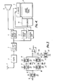
- Fig. 4 shows a general construction of a liquid crystal television receiver.
- Television signals sent from a broadcasting station are received by an antenna 1, and are converted in frequency by a tuner 2 to an intermediate frequency.
- the intermediate frequency signals are amplified and detected in signal processing circuit 3, and audio signals and video signals are obtained.
- the audio signals are delivered to a speaker 5 by way of an audio output circuit 4, while video signals are applied to a chroma stage 6 and a control unit 7.
- the chroma stage 6 comprises a chroma processing unit and chroma output unit, and the video signnals are demodulated into R, G, B signals in the chroma processing unit, and are converted into signals inverted in the polarity in every field by the chroma output unit to be applied to a Y driver IC 9.
- the video signals applied to the Y driver IC 9 are sample-held, and are applied to the source line of an active matrix liquid crystal panel 8.
- the video signals fed to the control unit 7, in which various control pulses are obtained are applied to the control signal input terminals of X driver IC 10 and Y driver IC 9.
- the X driver IC 10 is intended to scan in the vertical direction, and its output is applied to the gate line of active matrix liquid crystal panel 8. Thus, by the vertical direction scanning pulses from the X driver IC 10 and video signals from the Y driver IC 9, a television picture is obtained on the active matrix liquid crystal panel 8.
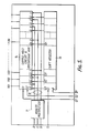
- Y driver IC 9 an example of composition of Y driver IC is shown in Fig. 5.
- the R, G, B signals from the chroma stage are applied to R, G, B terminals, and are changed over in every horizontal period by-an analog multiplexer 11 to be led into three video signal lines 12.
- the analog multiplexer 11 changes over according to the R, G, B picture element arrangement on the liquid crystal panel.
- Numeral 13 denotes a shift register, which receives clock ⁇ Y and start pulse S, and delivers sampling pulses Q,, Q 2 and so forth sequentialty.
- Numeral 14 denotes a sample and hold circuit and operational amplifier, which are designed to sample the video signals from the video signal line 12 according to the sample pulses Q,, Q 2 and so forth from the shift register, and hold them according to the pulses G 1 , G 1 elivers applied from outside.
- the outputs of the sample and hold circuit and operational amplifier 14 are connected to output terminals Y 01 , Y 02 ,.... of the Y driver IC and these output terminals are connected to the source line of the active matrix liquid crystal panel.
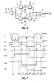
- Fig. 6 The sample and hold circuit and one (the n-th) of the operational amplifiers in Fig. 5 are shown in Fig. 6, in which numeral 15 denotes a video signal line, and 16 to 20 are switching circuits which operate to turn on when the pulse of the signal indicated by each arrow is high level, and turn off when it is low level.
- numeral 16 is a switching circuit for video signal sampling, and its output is applied to two input switching circuits 17, 18, and hold capacitors 22, 23 are connected to output switching circuits 19, 20 are connected to the output terminals of input switching circuit, while output terminals of hold capacitors.
- Output terminals of these two output switching circuits are mutually coupled together, and are connected to the input terminal of operational amplifier 21 having an input capacitance 24, and the output of operational amplifier becomes output Y on of Y driver IC, and is connected to the source line of liquid crystal panel.
- Waveforms of the sample and hold circuit and individual parts of operational amplifiers in Frg. 6 are shown in Fig. 7, in which V is a video signal applied to the video signal line 15, and one horizontal period is represented by H.
- G,, G 2 are control pulses applied to switching circuits 17 to 20 of sample hold, and the period of both G, and G 2 is 2H, and their phases are mutually deviated by ⁇ .
- ⁇ In order to perform the sample hold securely, there is a period t in which both G, and G2 are off.
- the period in which either G, or G 2 is on is indicated by t,, t 2 ,....
- Q n is an n-th output pulse of shift register 13, and it is a video signal sampling pulse to open or close the switching circuit 16.
- V na and V nb are voltage waveforms applied to hold capacitors 22, 23 and Y On is an n-th output waveform of Y driver IC.
- G2 is on and G, is off, so that the information V na of hold capacitor 22 is transmitted to the output Y on of Y driver IC, and video information V nb is sampled in the hold capacitor 23 by the sampling pulse of Q n .
- the information of V nb which has been sampled in t, period is transmitted to the output Y on of Y driver IC, while the video information V nais sampled in the hold capacitor 22 by the sampling pulse of Qn.
- the operations in the period of t,, t 2 are similarly repeated. '
- the input capacitance 24 is always present at the input side of operational amplifier 21, and when the operational amplifier is composed of CMOS, in particular, the value of input capacitance is considerably large.
- the value of input capacitance 24 of operational amplifier is generally too great to be ignored, and, therefore, when the output side switching circuits 19, 20 are turned on, the voltage being held by the hold capacitors 22, 23 is influenced by the electric charge 1 H before as being accumulated in the input capacitance 24 of the operational amplifier 21 in the output Y o , of Y driver IC, so that the input voltage may not be delivered at high fidelity.
- this invention is intended to present a sample and hold circuit which is capable of eliminating the adverse effects of the capacitance component if a capacitance component is present at the output side.
- This invention discloses a sample and hold circuit wherein a hold capacitor is connected between the output terminal of an input switching element and the reference potential, an output switching element for output is connected to the output terminal of the hold capacitor, and an output element connected to the output side of the output switching element and exhibiting a capacitance, characterised in that a discharge switching element which is made to conduct for a short period immediately before conduction of the output switching element, is provided in parallel with said capacitance of the output element whereby to discharge said capacitance.
- This invention having the above construction, can discharge the electric charge of the capacity component accumulated so far, by means of the switching element for discharge, immediately before the output from the hold capacity is applied to the capacity component of the output side, and can return the output potential to the reference potential so that the next hold voltage may be accurately delivered regardless of the previous output signal value.
- Fig. 1 shows the construction of a sample and hold circuit in the embodiment of this invention, in which numerals 15 to 24 corresponds to the parts of the conventional construction shown in Fig. 6.
- a switching circuit 25 which is turned on and off by P pulse is installed between the output side of the sample and hold circuit and reference potential.
- Fig. 2 shows the waveforms of various parts of the sample hold circuit in Fig. 1, in which a P pulse which is applied immediately before G, or G 2 is turned on so as to discharge the electric charge accumulated in the capacity component 24. That is, since the output Y on of the Y driver IC is returned to the reference potential when the P pulse is turned on, the voltage is always proportional to the sampled video signal regardless of the effect of the hold voltage 1H before. Therefore, as shown in Fig. 7 there is no step difference in the Y on value between t 2 period and t, period, and the voltage of same level is obtained.
- a sample and hold circuit capable of delivering outputs always correctly corresponding to the input video signals without being influenced by the video signal level 1 H before may be realized.
- each switching element is composed of parallel circuits of p-channel MOS and n-channel MOS.
- Q ⁇ n , G ⁇ 1 , G ⁇ 2 ,P ⁇ represent the polarity inverted pulses of Q n , G" G 2 , P respectively.
- the operational amplifier 21 is composed of aluminium bate CMOS, its input capacity 24 is about 0.4 to 1pF.
- the value of hold capacitors 22, 23 are several pF, effects of video signal level 1 H before may be present about 10 to 20% if there is no switching element 25.
- a sample and hold circuit capable of delivering outputs always correctly corresponding to the input video signal without being influenced by the video signal level 1 H before may be realized.
Abstract
Description
- This invention relates to a sample and hold circuit which may be used as a liquid crystal panel driving circuit or the like of a television receiver.
- Liquid crystal television receivers employing liquid crystal panels as display elements have been developed recently. To begin with, the outline of operation of such a liquid crystal television receiver is described below.
- Fig. 4 shows a general construction of a liquid crystal television receiver. Television signals sent from a broadcasting station are received by an
antenna 1, and are converted in frequency by atuner 2 to an intermediate frequency. The intermediate frequency signals are amplified and detected insignal processing circuit 3, and audio signals and video signals are obtained. The audio signals are delivered to aspeaker 5 by way of anaudio output circuit 4, while video signals are applied to achroma stage 6 and a control unit 7. Thechroma stage 6 comprises a chroma processing unit and chroma output unit, and the video signnals are demodulated into R, G, B signals in the chroma processing unit, and are converted into signals inverted in the polarity in every field by the chroma output unit to be applied to a Y driver IC 9. The video signals applied to the Y driver IC 9 are sample-held, and are applied to the source line of an active matrixliquid crystal panel 8. At the same time, the video signals fed to the control unit 7, in which various control pulses are obtained, are applied to the control signal input terminals ofX driver IC 10 and Y driver IC 9. The X driver IC 10 is intended to scan in the vertical direction, and its output is applied to the gate line of active matrixliquid crystal panel 8. Thus, by the vertical direction scanning pulses from theX driver IC 10 and video signals from the Y driver IC 9, a television picture is obtained on the active matrixliquid crystal panel 8. - Referring now to the outline of operation of Y driver IC 9 shown in Fig. 4, an example of composition of Y driver IC is shown in Fig. 5. The R, G, B signals from the chroma stage are applied to R, G, B terminals, and are changed over in every horizontal period by-an
analog multiplexer 11 to be led into threevideo signal lines 12. Theanalog multiplexer 11 changes over according to the R, G, B picture element arrangement on the liquid crystal panel. Numeral 13 denotes a shift register, which receives clock ØY and start pulse S, and delivers sampling pulses Q,, Q2 and so forth sequentialty. Numeral 14 denotes a sample and hold circuit and operational amplifier, which are designed to sample the video signals from thevideo signal line 12 according to the sample pulses Q,, Q2 and so forth from the shift register, and hold them according to the pulses G1, G1elivers applied from outside. The outputs of the sample and hold circuit andoperational amplifier 14 are connected to output terminals Y01, Y02,.... of the Y driver IC and these output terminals are connected to the source line of the active matrix liquid crystal panel. - The sample and hold circuit and one ( the n-th) of the operational amplifiers in Fig. 5 are shown in Fig. 6, in which
numeral 15 denotes a video signal line, and 16 to 20 are switching circuits which operate to turn on when the pulse of the signal indicated by each arrow is high level, and turn off when it is low level.Numeral 16 is a switching circuit for video signal sampling, and its output is applied to twoinput switching circuits capacitors output switching circuits operational amplifier 21 having aninput capacitance 24, and the output of operational amplifier becomes output Yon of Y driver IC, and is connected to the source line of liquid crystal panel. - In thus composed sample and hold circuit, the operation is as described below.
- Waveforms of the sample and hold circuit and individual parts of operational amplifiers in Frg. 6 are shown in Fig. 7, in which V is a video signal applied to the
video signal line 15, and one horizontal period is represented by H. G,, G2 are control pulses applied to switchingcircuits 17 to 20 of sample hold, and the period of both G, and G2 is 2H, and their phases are mutually deviated by π. In order to perform the sample hold securely, there is a period t in which both G, and G2 are off. The period in which either G, or G2 is on is indicated by t,, t2,.... Qn is an n-th output pulse ofshift register 13, and it is a video signal sampling pulse to open or close theswitching circuit 16. Vna and Vnb are voltage waveforms applied to holdcapacitors hold capacitor 22 is transmitted to the output Yon of Y driver IC, and video information Vnb is sampled in thehold capacitor 23 by the sampling pulse of Qn. Next. in the period of t2, when G, is on and G2 is off, the information of Vnb which has been sampled in t, period is transmitted to the output Yon of Y driver IC, while the video information V nais sampled in thehold capacitor 22 by the sampling pulse of Qn. Thereafter, in the period of t3, t4 and so forth, the operations in the period of t,, t2 are similarly repeated. ' - This arrangement, however, has the following problem. That is, the
input capacitance 24 is always present at the input side ofoperational amplifier 21, and when the operational amplifier is composed of CMOS, in particular, the value of input capacitance is considerably large. As compared with the valued ofhold capacitors input capacitance 24 of operational amplifier is generally too great to be ignored, and, therefore, when the outputside switching circuits hold capacitors electric charge 1 H before as being accumulated in theinput capacitance 24 of theoperational amplifier 21 in the output Yo, of Y driver IC, so that the input voltage may not be delivered at high fidelity. In the example shown in Fig. 7, the value of Yon in t2 period, which should be the voltage of the same level as in period t, as indicated by dot-dash line, is actually an upward shifted output voltage due to the effect of the operational amplifier input voltage in period t,. The above operation is explained in relation to a two branch construction of a sample and hold circuit, but the same holds true in a series connected one branch construction of a sample and hold circuit. Hence, the problem is, when the conventional sample and hold circuit and operational amplifier as shown in Fig. 6 are used, for example, in a liquid crystal televison, brightness changes occur where the brightness should be the same. - In the light of the above-discussed problem, this invention is intended to present a sample and hold circuit which is capable of eliminating the adverse effects of the capacitance component if a capacitance component is present at the output side.
- This invention discloses a sample and hold circuit wherein a hold capacitor is connected between the output terminal of an input switching element and the reference potential, an output switching element for output is connected to the output terminal of the hold capacitor, and an output element connected to the output side of the output switching element and exhibiting a capacitance, characterised in that a discharge switching element which is made to conduct for a short period immediately before conduction of the output switching element, is provided in parallel with said capacitance of the output element whereby to discharge said capacitance.
- This invention, having the above construction, can discharge the electric charge of the capacity component accumulated so far, by means of the switching element for discharge, immediately before the output from the hold capacity is applied to the capacity component of the output side, and can return the output potential to the reference potential so that the next hold voltage may be accurately delivered regardless of the previous output signal value.
- Features and advantages of the present invention will become more readily apparent from the following description of an embodiment thereof given by way of example with reference to the accompanying drawings in which:-
- Fig. 1 is a circuit diagram of a sample and hold circuit in accordance with one embodiment of this invention;
- Fig. 2 is a waveform diagram showing the waveforms of parts of the circuit shown in Fig. 1;
- Fig. 3 is a circuit diagram showing a practical example of the circuit shown in Fig. 1;
- Fig. 4 is a block diagram showing a general construction of a liquid crystal television receiver;
- Fig. 5 is a block diagram showing an example of Y driver IC construction;
- Fig. 6 is a circuit diagram of a conventional example of a sample and hold circuit; and
- Fig. 7 is a waveform diagram showing waveforms of parts of the same circuit.
- One of the embodiments of a sample and hold circuit of this invention is described below while referring to the accompanying drawings.
- Fig. 1 shows the construction of a sample and hold circuit in the embodiment of this invention, in which
numerals 15 to 24 corresponds to the parts of the conventional construction shown in Fig. 6. In this invention, aswitching circuit 25 which is turned on and off by P pulse is installed between the output side of the sample and hold circuit and reference potential. - The operation of such a sample and hold circuit is explained below by referring to Fig. 1 and Fig. 2.
- Fig. 2 shows the waveforms of various parts of the sample hold circuit in Fig. 1, in which a P pulse which is applied immediately before G, or G2 is turned on so as to discharge the electric charge accumulated in the
capacity component 24. That is, since the output Yon of the Y driver IC is returned to the reference potential when the P pulse is turned on, the voltage is always proportional to the sampled video signal regardless of the effect of thehold voltage 1H before. Therefore, as shown in Fig. 7 there is no step difference in the Y on value between t2 period and t, period, and the voltage of same level is obtained. - Thus, in this embodiment, by installing a switching element which conducts immediately before the switching element for output conducts, between the output circuit side of sample hold circuit and the reference potential, a sample and hold circuit capable of delivering outputs always correctly corresponding to the input video signals without being influenced by the
video signal level 1 H before may be realized. - The embodiment of this invention is shown in Fig. 3, in which each switching element is composed of parallel circuits of p-channel MOS and n-channel MOS. Q̅ n, G̅1, G̅2,P̅ represent the polarity inverted pulses of Qn, G" G2, P respectively. When the
operational amplifier 21 is composed of aluminium bate CMOS, itsinput capacity 24 is about 0.4 to 1pF. On the other hand, since the value ofhold capacitors video signal level 1 H before may be present about 10 to 20% if there is noswitching element 25. - The above explanation relates to two-branch construction of sample and hold circuit, but the same holds true with one-branch series connected construction. When this embodiment is applied in a liquid crystal television, it will be very effective.
- Thus, by this invention, by installing a switching element which conducts immediately before the switching element for output conducts between the output circuit side of a sample and hold circuit and reference potential, a sample and hold circuit capable of delivering outputs always correctly corresponding to the input video signal without being influenced by the
video signal level 1 H before may be realized.
Claims (6)
Applications Claiming Priority (2)
| Application Number | Priority Date | Filing Date | Title |
|---|---|---|---|
| JP75602/85 | 1985-04-10 | ||
| JP60075602A JPH0654961B2 (en) | 1985-04-10 | 1985-04-10 | Sample-hold circuit |
Publications (3)
| Publication Number | Publication Date |
|---|---|
| EP0200402A2 true EP0200402A2 (en) | 1986-11-05 |
| EP0200402A3 EP0200402A3 (en) | 1988-07-06 |
| EP0200402B1 EP0200402B1 (en) | 1991-08-14 |
Family
ID=13580915
Family Applications (1)
| Application Number | Title | Priority Date | Filing Date |
|---|---|---|---|
| EP86302684A Expired EP0200402B1 (en) | 1985-04-10 | 1986-04-10 | Sample and hold circuit |
Country Status (4)
| Country | Link |
|---|---|
| US (1) | US4823027A (en) |
| EP (1) | EP0200402B1 (en) |
| JP (1) | JPH0654961B2 (en) |
| DE (1) | DE3680816D1 (en) |
Cited By (1)
| Publication number | Priority date | Publication date | Assignee | Title |
|---|---|---|---|---|
| EP0741391A2 (en) * | 1990-01-26 | 1996-11-06 | Kabushiki Kaisha Toshiba | Sample-and-hold circuit device |
Families Citing this family (27)
| Publication number | Priority date | Publication date | Assignee | Title |
|---|---|---|---|---|
| JPH0289438A (en) * | 1988-09-27 | 1990-03-29 | Toshiba Corp | Sampling circuit |
| JP2576606B2 (en) * | 1988-10-13 | 1997-01-29 | 日本電気株式会社 | Output driver circuit |
| US4987321A (en) * | 1989-09-25 | 1991-01-22 | Eastman Kodak Company | Processing circuit for image sensor |
| US5111072A (en) * | 1990-08-29 | 1992-05-05 | Ncr Corporation | Sample-and-hold switch with low on resistance and reduced charge injection |
| FR2667188A1 (en) * | 1990-09-21 | 1992-03-27 | Senn Patrice | SAMPLE-LOCKER CIRCUIT FOR LIQUID CRYSTAL DISPLAY SCREEN. |
| KR930004268B1 (en) * | 1990-10-15 | 1993-05-22 | 금성일렉트론 주식회사 | Broad band sample & hold circuit |
| JPH04179996A (en) * | 1990-11-15 | 1992-06-26 | Toshiba Corp | Sample-hold circuit and liquid crystal display device using the same |
| JP2833289B2 (en) * | 1991-10-01 | 1998-12-09 | 日本電気株式会社 | Analog switch |
| JP3067059B2 (en) * | 1992-07-09 | 2000-07-17 | シャープ株式会社 | Sample hold circuit |
| JP2558586B2 (en) * | 1993-01-11 | 1996-11-27 | キャスコ株式会社 | Golf ball |
| US5281867A (en) * | 1993-02-23 | 1994-01-25 | Motorola, Inc. | Multiple channel sampling circuit having minimized crosstalk interference |
| US5644257A (en) * | 1993-03-24 | 1997-07-01 | Crystal Semiconductor Corporation | Sampling circuit charge management |
| US5418533A (en) * | 1993-11-19 | 1995-05-23 | Tektronix, Inc. | Method and circuit for conditioning a signal for use in systems having analog-to-digital converter circuits |
| JP2747230B2 (en) * | 1994-10-04 | 1998-05-06 | ローム株式会社 | Signal processing device |
| US6031398A (en) * | 1997-01-22 | 2000-02-29 | Lucent Technologies Inc. | Reduced-feedthrough switch circuit |
| EP0862270A1 (en) * | 1997-02-28 | 1998-09-02 | STMicroelectronics S.r.l. | Staircase adaptive voltage generator circuit |
| US5963063A (en) * | 1997-08-26 | 1999-10-05 | Texas Instruments Incorporated | Sample and hold circuit having a waveform shaping circuit |
| DE19753279C2 (en) * | 1997-12-01 | 2001-03-08 | Sgs Thomson Microelectronics | Electrical circuit with at least one switched capacitor and method for operating this circuit |
| US6963321B2 (en) * | 2001-05-09 | 2005-11-08 | Clare Micronix Integrated Systems, Inc. | Method of providing pulse amplitude modulation for OLED display drivers |
| WO2003034389A2 (en) * | 2001-10-19 | 2003-04-24 | Clare Micronix Integrated Systems, Inc. | System and method for providing pulse amplitude modulation for oled display drivers |
| JP4046015B2 (en) * | 2002-06-07 | 2008-02-13 | セイコーエプソン株式会社 | Electronic circuit, electronic device, electro-optical device, and electronic apparatus |
| US7170041B2 (en) * | 2002-07-17 | 2007-01-30 | Xerox Corporation | Pixel circuitry for imaging system |
| AU2003280128A1 (en) * | 2002-11-25 | 2004-06-18 | Koninklijke Philips Electronics N.V. | Sample and hold circuit |
| JP4536452B2 (en) * | 2004-08-04 | 2010-09-01 | ルネサスエレクトロニクス株式会社 | Semiconductor integrated circuit and method for supplying power supply voltage to semiconductor integrated circuit |
| US7683677B2 (en) * | 2007-08-06 | 2010-03-23 | Mediatek Inc. | Sample-and-hold amplification circuits |
| JP5102131B2 (en) * | 2008-07-14 | 2012-12-19 | 株式会社豊田中央研究所 | Hold circuit |
| JP6179718B2 (en) * | 2013-10-01 | 2017-08-16 | セイコーNpc株式会社 | Sample hold circuit |
Citations (3)
| Publication number | Priority date | Publication date | Assignee | Title |
|---|---|---|---|---|
| GB2068189A (en) * | 1980-01-14 | 1981-08-05 | Western Electric Co | Amplifiers |
| US4366456A (en) * | 1979-06-14 | 1982-12-28 | Fujitsu Limited | Switched-capacitor filter |
| US4430622A (en) * | 1981-11-19 | 1984-02-07 | Gte Laboratories Incorporated | Offset correction circuit |
Family Cites Families (5)
| Publication number | Priority date | Publication date | Assignee | Title |
|---|---|---|---|---|
| US3226650A (en) * | 1964-03-09 | 1965-12-28 | Thomas E Higbie | Video pulse amplitude detector for airborne radar systems |
| JPS5842683B2 (en) * | 1973-05-08 | 1983-09-21 | トヨタ精機工業 (株) | Steel plate round electric wire junction box manufacturing method |
| FR2453471A1 (en) * | 1979-04-06 | 1980-10-31 | Inst Francais Du Petrole | IMPROVED SAMPLER-LOCKER |
| JPS5884342A (en) * | 1981-11-13 | 1983-05-20 | Toshiba Corp | Signal processing circuit |
| JPS60214177A (en) * | 1984-04-09 | 1985-10-26 | Sharp Corp | Liquid crystal drive circuit |
-
1985
- 1985-04-10 JP JP60075602A patent/JPH0654961B2/en not_active Expired - Lifetime
-
1986
- 1986-04-10 EP EP86302684A patent/EP0200402B1/en not_active Expired
- 1986-04-10 DE DE8686302684T patent/DE3680816D1/en not_active Expired - Lifetime
-
1987
- 1987-10-19 US US07/111,093 patent/US4823027A/en not_active Expired - Lifetime
Patent Citations (3)
| Publication number | Priority date | Publication date | Assignee | Title |
|---|---|---|---|---|
| US4366456A (en) * | 1979-06-14 | 1982-12-28 | Fujitsu Limited | Switched-capacitor filter |
| GB2068189A (en) * | 1980-01-14 | 1981-08-05 | Western Electric Co | Amplifiers |
| US4430622A (en) * | 1981-11-19 | 1984-02-07 | Gte Laboratories Incorporated | Offset correction circuit |
Non-Patent Citations (1)
| Title |
|---|
| ELECTRONICS, vol. 46, no. 20, 27th September 1973, pages 127-128, New York US; J.E. BUCHANAN: "C-MOS switch speeds up sample-and-hold circuit" * |
Cited By (2)
| Publication number | Priority date | Publication date | Assignee | Title |
|---|---|---|---|---|
| EP0741391A2 (en) * | 1990-01-26 | 1996-11-06 | Kabushiki Kaisha Toshiba | Sample-and-hold circuit device |
| EP0741391A3 (en) * | 1990-01-26 | 1996-11-13 | Kabushiki Kaisha Toshiba | Sample-and-hold circuit device |
Also Published As
| Publication number | Publication date |
|---|---|
| JPS61234674A (en) | 1986-10-18 |
| EP0200402B1 (en) | 1991-08-14 |
| EP0200402A3 (en) | 1988-07-06 |
| JPH0654961B2 (en) | 1994-07-20 |
| US4823027A (en) | 1989-04-18 |
| DE3680816D1 (en) | 1991-09-19 |
Similar Documents
| Publication | Publication Date | Title |
|---|---|---|
| EP0200402A2 (en) | Sample and hold circuit | |
| US4591902A (en) | Matrix type color television panel driver circuit | |
| US5721563A (en) | Active matrix liquid crystal drive circuit capable of correcting offset voltage | |
| KR940008178B1 (en) | Sample hold circuit and liquid crystal display apparatus | |
| KR0142414B1 (en) | The liquid crystal display device | |
| EP0741391B1 (en) | Sample-and-hold circuit device | |
| US4734692A (en) | Driver circuit for liquid crystal display | |
| KR100420229B1 (en) | A video signal application device, a comparator for a data line driver of a display device, and a video device | |
| JPH0654421B2 (en) | Column electrode driving circuit of matrix type liquid crystal display device | |
| JPH0776866B2 (en) | Driving circuit in liquid crystal display device | |
| EP0192784B1 (en) | Liquid crystal display device | |
| KR890004241B1 (en) | Television video signal a/d converter apparatus | |
| JPH07118795B2 (en) | Driving method for liquid crystal display device | |
| US7427880B2 (en) | Sample/hold apparatus with small-sized capacitor and its driving method | |
| EP0737958A2 (en) | Video driver for a display apparatus | |
| US5252956A (en) | Sample and hold circuit for a liquid crystal display screen | |
| US4954703A (en) | Color line sensor apparatus | |
| US4660085A (en) | Television receiver responsive to plural video signals | |
| US5497201A (en) | Sync chip clamping/sync separator circuit | |
| JPS62142480A (en) | Liquid crystal panel drive circuit | |
| JPH03235989A (en) | Liquid crystal display device | |
| JPS5952589B2 (en) | timing signal generator | |
| KR960003963B1 (en) | Driving integration circuit for lcd | |
| JPH0654418B2 (en) | Control pulse generation circuit for LCD panel drive | |
| JPH06186925A (en) | Driving circuit for display device |
Legal Events
| Date | Code | Title | Description |
|---|---|---|---|
| PUAI | Public reference made under article 153(3) epc to a published international application that has entered the european phase |
Free format text: ORIGINAL CODE: 0009012 |
|
| AK | Designated contracting states |
Kind code of ref document: A2 Designated state(s): DE FR GB |
|
| PUAB | Information related to the publication of an a document modified or deleted |
Free format text: ORIGINAL CODE: 0009199EPPU |
|
| RA1 | Application published (corrected) |
Date of ref document: 19861210 Kind code of ref document: A2 |
|
| PUAL | Search report despatched |
Free format text: ORIGINAL CODE: 0009013 |
|
| AK | Designated contracting states |
Kind code of ref document: A3 Designated state(s): DE FR GB |
|
| 17P | Request for examination filed |
Effective date: 19881221 |
|
| 17Q | First examination report despatched |
Effective date: 19900531 |
|
| GRAA | (expected) grant |
Free format text: ORIGINAL CODE: 0009210 |
|
| AK | Designated contracting states |
Kind code of ref document: B1 Designated state(s): DE FR GB |
|
| REF | Corresponds to: |
Ref document number: 3680816 Country of ref document: DE Date of ref document: 19910919 |
|
| ET | Fr: translation filed | ||
| PLBE | No opposition filed within time limit |
Free format text: ORIGINAL CODE: 0009261 |
|
| STAA | Information on the status of an ep patent application or granted ep patent |
Free format text: STATUS: NO OPPOSITION FILED WITHIN TIME LIMIT |
|
| 26N | No opposition filed | ||
| PGFP | Annual fee paid to national office [announced via postgrant information from national office to epo] |
Ref country code: GB Payment date: 19960401 Year of fee payment: 11 |
|
| PGFP | Annual fee paid to national office [announced via postgrant information from national office to epo] |
Ref country code: FR Payment date: 19960410 Year of fee payment: 11 |
|
| PGFP | Annual fee paid to national office [announced via postgrant information from national office to epo] |
Ref country code: DE Payment date: 19960418 Year of fee payment: 11 |
|
| PG25 | Lapsed in a contracting state [announced via postgrant information from national office to epo] |
Ref country code: GB Effective date: 19970410 |
|
| GBPC | Gb: european patent ceased through non-payment of renewal fee |
Effective date: 19970410 |
|
| PG25 | Lapsed in a contracting state [announced via postgrant information from national office to epo] |
Ref country code: FR Free format text: LAPSE BECAUSE OF NON-PAYMENT OF DUE FEES Effective date: 19971231 |
|
| PG25 | Lapsed in a contracting state [announced via postgrant information from national office to epo] |
Ref country code: DE Free format text: LAPSE BECAUSE OF NON-PAYMENT OF DUE FEES Effective date: 19980101 |
|
| REG | Reference to a national code |
Ref country code: FR Ref legal event code: ST |