EP0198590A2 - Semiconductor memory device - Google Patents
Semiconductor memory device Download PDFInfo
- Publication number
- EP0198590A2 EP0198590A2 EP86301758A EP86301758A EP0198590A2 EP 0198590 A2 EP0198590 A2 EP 0198590A2 EP 86301758 A EP86301758 A EP 86301758A EP 86301758 A EP86301758 A EP 86301758A EP 0198590 A2 EP0198590 A2 EP 0198590A2
- Authority
- EP
- European Patent Office
- Prior art keywords
- layer
- island
- capacitor
- semiconductor
- groove
- Prior art date
- Legal status (The legal status is an assumption and is not a legal conclusion. Google has not performed a legal analysis and makes no representation as to the accuracy of the status listed.)
- Granted
Links
- 239000004065 semiconductor Substances 0.000 title claims abstract description 49
- 239000003990 capacitor Substances 0.000 claims abstract description 71
- 230000015654 memory Effects 0.000 claims abstract description 45
- 239000000758 substrate Substances 0.000 claims abstract description 27
- 238000004519 manufacturing process Methods 0.000 claims description 16
- 238000000034 method Methods 0.000 claims description 16
- 239000012535 impurity Substances 0.000 claims description 10
- XUIMIQQOPSSXEZ-UHFFFAOYSA-N Silicon Chemical compound [Si] XUIMIQQOPSSXEZ-UHFFFAOYSA-N 0.000 abstract description 4
- 229910052710 silicon Inorganic materials 0.000 abstract description 4
- 239000010703 silicon Substances 0.000 abstract description 4
- 108010075750 P-Type Calcium Channels Proteins 0.000 abstract 1
- 238000012856 packing Methods 0.000 description 11
- 230000003247 decreasing effect Effects 0.000 description 10
- 229910021420 polycrystalline silicon Inorganic materials 0.000 description 8
- 230000007423 decrease Effects 0.000 description 7
- 238000010586 diagram Methods 0.000 description 7
- 239000011159 matrix material Substances 0.000 description 5
- 230000006872 improvement Effects 0.000 description 4
- 238000001020 plasma etching Methods 0.000 description 4
- VYPSYNLAJGMNEJ-UHFFFAOYSA-N Silicium dioxide Chemical compound O=[Si]=O VYPSYNLAJGMNEJ-UHFFFAOYSA-N 0.000 description 3
- 238000003491 array Methods 0.000 description 3
- 230000015572 biosynthetic process Effects 0.000 description 3
- 230000000873 masking effect Effects 0.000 description 3
- 229910052751 metal Inorganic materials 0.000 description 3
- 239000002184 metal Substances 0.000 description 3
- 229910052782 aluminium Inorganic materials 0.000 description 2
- XAGFODPZIPBFFR-UHFFFAOYSA-N aluminium Chemical compound [Al] XAGFODPZIPBFFR-UHFFFAOYSA-N 0.000 description 2
- 238000009792 diffusion process Methods 0.000 description 2
- 238000005530 etching Methods 0.000 description 2
- 239000011810 insulating material Substances 0.000 description 2
- 239000000463 material Substances 0.000 description 2
- 229920002120 photoresistant polymer Polymers 0.000 description 2
- 229910052814 silicon oxide Inorganic materials 0.000 description 2
- 238000001039 wet etching Methods 0.000 description 2
- ZOXJGFHDIHLPTG-UHFFFAOYSA-N Boron Chemical compound [B] ZOXJGFHDIHLPTG-UHFFFAOYSA-N 0.000 description 1
- 238000000137 annealing Methods 0.000 description 1
- 229910052785 arsenic Inorganic materials 0.000 description 1
- RQNWIZPPADIBDY-UHFFFAOYSA-N arsenic atom Chemical compound [As] RQNWIZPPADIBDY-UHFFFAOYSA-N 0.000 description 1
- 229910052796 boron Inorganic materials 0.000 description 1
- 230000015556 catabolic process Effects 0.000 description 1
- 230000008859 change Effects 0.000 description 1
- 150000001875 compounds Chemical class 0.000 description 1
- 238000006731 degradation reaction Methods 0.000 description 1
- 230000000593 degrading effect Effects 0.000 description 1
- 238000011161 development Methods 0.000 description 1
- 230000018109 developmental process Effects 0.000 description 1
- 238000007599 discharging Methods 0.000 description 1
- 238000009826 distribution Methods 0.000 description 1
- 230000005669 field effect Effects 0.000 description 1
- 230000006870 function Effects 0.000 description 1
- BHEPBYXIRTUNPN-UHFFFAOYSA-N hydridophosphorus(.) (triplet) Chemical compound [PH] BHEPBYXIRTUNPN-UHFFFAOYSA-N 0.000 description 1
- 230000001771 impaired effect Effects 0.000 description 1
- 238000005468 ion implantation Methods 0.000 description 1
- 229910044991 metal oxide Inorganic materials 0.000 description 1
- 150000004706 metal oxides Chemical class 0.000 description 1
- 238000012986 modification Methods 0.000 description 1
- 230000004048 modification Effects 0.000 description 1
- 238000012545 processing Methods 0.000 description 1
- 150000003377 silicon compounds Chemical class 0.000 description 1
Images


Classifications
-
- H—ELECTRICITY
- H10—SEMICONDUCTOR DEVICES; ELECTRIC SOLID-STATE DEVICES NOT OTHERWISE PROVIDED FOR
- H10B—ELECTRONIC MEMORY DEVICES
- H10B12/00—Dynamic random access memory [DRAM] devices
-
- H—ELECTRICITY
- H01—ELECTRIC ELEMENTS
- H01L—SEMICONDUCTOR DEVICES NOT COVERED BY CLASS H10
- H01L29/00—Semiconductor devices adapted for rectifying, amplifying, oscillating or switching, or capacitors or resistors with at least one potential-jump barrier or surface barrier, e.g. PN junction depletion layer or carrier concentration layer; Details of semiconductor bodies or of electrodes thereof ; Multistep manufacturing processes therefor
- H01L29/02—Semiconductor bodies ; Multistep manufacturing processes therefor
- H01L29/06—Semiconductor bodies ; Multistep manufacturing processes therefor characterised by their shape; characterised by the shapes, relative sizes, or dispositions of the semiconductor regions ; characterised by the concentration or distribution of impurities within semiconductor regions
- H01L29/0684—Semiconductor bodies ; Multistep manufacturing processes therefor characterised by their shape; characterised by the shapes, relative sizes, or dispositions of the semiconductor regions ; characterised by the concentration or distribution of impurities within semiconductor regions characterised by the shape, relative sizes or dispositions of the semiconductor regions or junctions between the regions
- H01L29/0692—Surface layout
-
- H—ELECTRICITY
- H01—ELECTRIC ELEMENTS
- H01L—SEMICONDUCTOR DEVICES NOT COVERED BY CLASS H10
- H01L29/00—Semiconductor devices adapted for rectifying, amplifying, oscillating or switching, or capacitors or resistors with at least one potential-jump barrier or surface barrier, e.g. PN junction depletion layer or carrier concentration layer; Details of semiconductor bodies or of electrodes thereof ; Multistep manufacturing processes therefor
- H01L29/66—Types of semiconductor device ; Multistep manufacturing processes therefor
- H01L29/68—Types of semiconductor device ; Multistep manufacturing processes therefor controllable by only the electric current supplied, or only the electric potential applied, to an electrode which does not carry the current to be rectified, amplified or switched
- H01L29/76—Unipolar devices, e.g. field effect transistors
- H01L29/772—Field effect transistors
- H01L29/78—Field effect transistors with field effect produced by an insulated gate
- H01L29/7827—Vertical transistors
-
- H—ELECTRICITY
- H01—ELECTRIC ELEMENTS
- H01L—SEMICONDUCTOR DEVICES NOT COVERED BY CLASS H10
- H01L29/00—Semiconductor devices adapted for rectifying, amplifying, oscillating or switching, or capacitors or resistors with at least one potential-jump barrier or surface barrier, e.g. PN junction depletion layer or carrier concentration layer; Details of semiconductor bodies or of electrodes thereof ; Multistep manufacturing processes therefor
- H01L29/66—Types of semiconductor device ; Multistep manufacturing processes therefor
- H01L29/86—Types of semiconductor device ; Multistep manufacturing processes therefor controllable only by variation of the electric current supplied, or only the electric potential applied, to one or more of the electrodes carrying the current to be rectified, amplified, oscillated or switched
- H01L29/92—Capacitors with potential-jump barrier or surface barrier
- H01L29/94—Metal-insulator-semiconductors, e.g. MOS
- H01L29/945—Trench capacitors
-
- H—ELECTRICITY
- H10—SEMICONDUCTOR DEVICES; ELECTRIC SOLID-STATE DEVICES NOT OTHERWISE PROVIDED FOR
- H10B—ELECTRONIC MEMORY DEVICES
- H10B12/00—Dynamic random access memory [DRAM] devices
- H10B12/01—Manufacture or treatment
- H10B12/02—Manufacture or treatment for one transistor one-capacitor [1T-1C] memory cells
- H10B12/03—Making the capacitor or connections thereto
- H10B12/038—Making the capacitor or connections thereto the capacitor being in a trench in the substrate
- H10B12/0383—Making the capacitor or connections thereto the capacitor being in a trench in the substrate wherein the transistor is vertical
-
- H—ELECTRICITY
- H10—SEMICONDUCTOR DEVICES; ELECTRIC SOLID-STATE DEVICES NOT OTHERWISE PROVIDED FOR
- H10B—ELECTRONIC MEMORY DEVICES
- H10B12/00—Dynamic random access memory [DRAM] devices
- H10B12/30—DRAM devices comprising one-transistor - one-capacitor [1T-1C] memory cells
- H10B12/39—DRAM devices comprising one-transistor - one-capacitor [1T-1C] memory cells the capacitor and the transistor being in a same trench
- H10B12/395—DRAM devices comprising one-transistor - one-capacitor [1T-1C] memory cells the capacitor and the transistor being in a same trench the transistor being vertical
Definitions
- the present invention relates to semiconductor memory devices and, more particularly, to a dynamic semiconductor memory device each cell of which consists of a transistor and a capacitor.
- Dynamic random access memories (to be referred to as dRAMs hereinafter) are represented by a MOS dRAM having cells each consisting of a MOS capacitor and a MOS transistor (MOSFET).
- MOSFET MOS transistor
- "1" or "0" digital data is stored in accordance with whether a charge is stored in its MOS capacitor or not. This data is read out by discharging the charge stored in the MOS capacitor of a selected cell to a corresponding bit line through a MOSFET and detecting a change in the potential of that bit line.
- a dRAM can have a large memory capacity when packing density (i.e., density of memory cells) in chips of the same size is increased.
- the packing density of MOS dRAMs has been greatly improved due to new developments in recent semi-conductor, manufacturing techniques, particularly in micropatterning. As a result, it may be considered that a dRAM having a large memory capacity can be easily obtained by decreasing cell size on a chip substrate and increasing cell density.
- the charging amount of the cell capacitor depends not only on the capacitance of the MOS capacitor but also on the value of the voltage applied thereto. It is theoretically possible to improve the charging amount of the cell capacitor by increasing the voltage applied thereto. In practice, however, increase in the applied voltage is not preferred since it requires increase in the power source voltage of the dRAM, which results in an increase in power consumption.
- method (1) is limited in its application to a dRAM manufacturing process since the thickness of the gate insulating layer cannot be decreased drastically without degrading the reliability of the element characteristics. Therefore, method (1) cannot be adopted.
- method (2) an insulating material having large dielectric constant E would be used in place of silicon oxide (Si02), which is currently under widespread use.
- Si02 silicon oxide
- no insulating material has yet been found which satisfies the above conditions and which can replace silicon oxide (a silicon compound such as Si,N ⁇ may be proposed as a substitute, but there are inherent problems in using such a compound in the mass production of highly reliable dRAMs.) Therefore, method (2) cannot be adopted, either.
- method (3) i.e., a method to increase the area of the capacitor electrode, must be adopted.
- cell capacitors are conventionally formed in grooves for separating cell regions on a substrate. More specifically, the cell capacitors are formed not on the cell regions defined by the grooves but in the grooves surrounding the island cell regions. In this case, the electrode of each cell capacitor also extends vertically along-a recessed section of the groove. Therefore, the area of the capacitor electrode is substantially increased despite the small area of the grooves, resulting in great improvements in the effective capacitance of the cell capacitor.
- the area of the cell region is increased, and an expected improvement in higher packing density (larger memory capacity) of the dRAM cannot be obtained.
- the cell transistor is constituted by a gate electrode provided on a periphery of the island cell region and a drain region formed at a central portion of the cell region. Therefore, the area of the MOS transistor in the cell is undesirably increased, and it is still difficult to enable a dRAM having good operational reliability and a large memory capacity (high packing density).
- an object of the present invention to provide a new and improved semiconductor memory device having a large memory capacity, in which cells having superior electrical characteristics can be formed on a substrate at a high packing density.
- a semiconductor substrate of a first conductivity type is provided with grooves.
- Each memory cell consists of a single capacitor and a single transistor, and the memory cell capacitors are buried in the grooves.
- Each cell capacitor has a capacitor electrode layer insulatively provided above the bottom surface of the groove, and a semiconductor layer of a second conductivity type formed on a lower surface region of the side wall of one island layer. This semiconductor layer . opposes the capacitor electrode layer to store charges therebetween, thereby constituting the memory cell capacitor.
- the cell transistor is also formed using the side wall of the groove. More specifically, active layers of the transistor are formed to be vertically stacked with the semiconductor layer of the capacitor, using as much of the side wall of the island layer as possible.
- the drain layer of the transistor is formed on the top surface region of the island layer.
- Other active layers such as a channel layer, are formed on the surface region of the side wall of the island layer.
- the gate electrode of the transistor is buried in a corresponding groove so as to oppose the channel layer and be stacked with the capacitor electrode layer. With this arrangement, the memory packing density of the device is increased without decreasing the capacitance of the memory capacitor, thus achieving the above object.
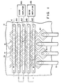
- Fig. 1 shows a plan configuration of the main portion of a MOS dynamic random access memory (dRAM) according to one embodiment of the present invention. Note that an oxide film layer and other arrangements obvious to one skilled in the art are omitted in Fig. 1 for the sake of simplicity.
- dRAM MOS dynamic random access memory
- substrate 10 is comprised of a p +- type semiconductor material such as silicon.
- the surface of substrate 10 is provided with a plurality of grooves 12, which define isolated island layers 14.
- Each layer 14 consists of a p--type semiconductor material such as silicon.
- Island layers 14 serves as independent cell regions 14, each of which is shaped in a rectangular parallelepiped so that it has a rectangular (e.g.,square) top surface region and four substantially vertical side walls. In this embodiment, one memory cell is provided in each cell region 14.
- the dRAM of this embodiment has a so-called "folded bit line arrangement".
- the columns (cells vertically aligned in Fig. 1) of layers 14 are offset alternately by half of the cell pitch.
- Bit lines 16 extend on the columns of island layers 14 in the row direction (horizontal in Fig. 1) to be substantially perpendicular thereto. Lines 16 connect corresponding island cell regions in every other columns.
- Two adjacent lit lines e.g., lines 16a and 16a'
- Pairs of bit lines 16a and 16a', 16b and 16b', etc., connected to each other are connected to sense amplifiers 18a, 18b, etc.
- Word lines 19 extending in the column direction (vertical in Fig. 1) are connected to the columns of island cell regions 14.
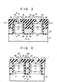
- Fig. 2 shows a sectional arrangement of the dRAM taken along the line 11 -11 of Fig. 1, and shows two island cell layers 14-1 and 14-2 included in two adjacent memory cell columns.
- one memory cell corresponds to one layer 14 in this embodiment.
- Each memory cell consists of single metal oxide semiconductor - (MOS) capacitor C and field effect transistor (MOSFET) Q.
- MOS metal oxide semiconductor -
- MOSFET field effect transistor
- layer 14-1 will now be described in detail (other memory cells not described here have the same arrangements).
- portions of layer 14-2 that are equivalent to those of layer 14-1 are denoted by the same reference numerals with "'", for the sake of simplicity.
- N-type semiconductor layer 20 is formed on the lower half surface region of the side wall of layer 14-1.
- Layer 20 extends entirely along the side walls of the lower half of layer 14-1 (i.e., to surround the lower half of the four side walls).
- a conductive layer, such as metal layer 22, is buried in groove 12 at the sides of layer 14-1, so as to oppose layer 20. More specifically, layer 22 is formed in a square shape to surround square layer 20 on its outer side surfaces.
- the width of layer 22 substantially corresponds to the width of groove 12.
- the height of metal layer 22 substantially corresponds to the height of layer 20.
- the height of layer 20 must not be smaller than that of layer 22.
- Layer 22 serves as a capacitor electrode of memory cell capacitor C. Insulative layer 24 is filled between layers 20 and 22 to provide a capacitive component therebetween. Layer 22 is integrally formed with the capacitor electrode layers in other memory cells of other layers 14, and constitutes a common capacitor electrode.
- P--type semiconductor layer 26 is formed on the upper half of the side walls of layer 14-1.
- the impurity concentration of layer 26 is higher than that of layer 14 by about 10 2 .
- Substantially square-ring-shaped layer 26 extends along the entire side walls of the upper half of layer 14-1 (i.e., to surround the four side walls) and is in electrical contact with layer 20.
- Layer 26 serves as a channel region of memory cell transistor Q.
- a conductive layer, such as metal layer 28 is buried in groove 12 so as to oppose and surround layer 26 on its outer side surfaces.
- Layer 28 commonly surrounds layers 14 in the same cell column and serves as a gate electrode of memory cell transistor Q and a word line within the cell matrix. Insulative layer 30 is filled between layers 26 and 28 to separate them electrically .
- N I- type semiconductor layer 32 is formed in a top surface region of layer 14-1.
- Layer 32 covers the entire surface of layer 14-1 and functions as a drain layer of cell transistor Q.
- layer 20 of capacitor C described above also serves as a source layer of transistor Q.
- lnsulative layer 34 made of a CVD oxide film is formed to bury the above arrangement.
- Layer 34 is provided with contact hole 36 at substantially the central portion of each drain layer 32 formed in the top surface of each layer 14.
- Bit lines 16 shown in Fig. 1 consist of a plurality of aluminum layers and extend parallel to each other to connect holes 32.
- drain layers 32 of cell transistors Q aligned in the row direction (horizontal in Fig. 1) of every other cell columns (i.e., vertical cell arrays in Fig. 1). are connected to each other through corresponding bit lines 16.
- FIG. 3 a sectional arrangement of adjacent layers 14 in a single cell column is shown in detail. It is clearly understood from Fig. 3 that gate electrode layers 28 for MOSFETs of cells in the same column are connected in common with each other. Single gate electrode layer 28 is buried in groove 12 to simultaneously surround channel regions 26 and 26' formed in the side walls of adjacent island cell layers 14, as shown in Fig. 3.
- layer 28 serving as the gate electrode layer is formed (in an inverted container manner) so as to not only surround the four side walls of each island layer 14 but to also cover the top surface thereof, as indicated by broken line 40 in Fig. 1.
- An insulating layer (not shown), having an identical hole to layer 34 with hole 36, is formed on gate electrode layer 28.
- Each word line 19 overlaps this contact hole in the insulating layer of last layer 14 in each column.
- respective word lines 19 outside the cell matrix are electrically connected to gate layers 28 of last layers 14 in columns.
- the dRAM according to the first embodiment of the present invention described above not only cell capacitors C but also most of cell transistors Q are located in grooves 12, using the side walls of isolated layers 14. Only drain layer 32 of transistor Qis-formed on the top surface region of each layer 14. Accordingly, the area of each layer 14 can be smaller than that in a conventional arrangement and the number of layers 14 on one chip substrate 10 can be greatly increased. As a result, the packing density of the memory can be improved, enabling a dRAM having a large memory capacity.
- the present inventor experimentally manufactured an actual dRAM having a memory capacity about four times that of a conventional dRAM, on the same chip size.
- the capacitance of cell capacitor C is not impaired upon improvement in the packing density of the memory. This is because the effective electrode area of capacitors C buried in grooves 12 defining layers 14 is not at all influenced by decrease in the area of the layers 14. Since the effective electrode area of cell capacitors C is not decreased, the capacitance thereof can be made as large as is required, based on high reliability of the memory. As a result, a dRAM having high operating reliability as well as large memory capacity can be provided.
- cell transistors Q as well as cell capacitors C are partially buried in grooves 12 (specifically, the gate electrodes are formed therein), so that the surface configuration of the dRAM can be flattened.
- fine wiring patterns can be manufactured easily in subsequent wiring steps. This contributes to higher packing density and further improvement in reliability of the dRAM having a large memory capacity.
- FIG. 4A to 4H correspond to a section taken along the line III -111 of Fig. 1 and respectively show structures obtained in major steps of the manufacturing method according to the present invention.
- the same reference numerals in Figs. 4A to 4H denote the same parts as in Figs. 1 to 3.
- p--type semiconductor layer 50 is epitaxially grown on p +- type silicon substrate 10.
- Mask layer 52 is deposited on layer 50, and photoresist film 54 is deposited thereon.
- Film 54 is patterned to have a predetermined pattern by a known method and layer 52 is etched using film 54 as a mask, thereby obtaining the structure shown in Fig. 4A.
- Layer 50 is etched using layer 52 shown in Fig. 4A so that grooves 12 defining a plurality of island cell layers 14 are formed on layer 50, as shown in Fig. 4B. Grooves 12 completely penetrate layer 50 to reach the upper surface of substrate 10. In this embodiment, grooves 12 are formed to extend into the upper surface region of substrate 10. The- depth of recess 55 thus formed in substrate 10 substantially corresponds to the thickness of an insulative layer (58) to be formed later.
- An oxide film containing phosphorous is deposited on the entire surface of the substrate body having the above configuration. The oxide film is annealed to form n--type layer 56 (which serves as semiconductor layer 20 afterwards constituting cell capacitor C) on the entire surface region around each layer 14. Thereafter, thin oxide film 58 of about 10 nm is formed to cover each layer 14. Note that film 58 is also formed in recess 55 and is thus flush with the upper surface of substrate 10. This maximizes of the capacitance of cell capacitor C.
- first polycrystalline silicon layer 60 is deposited on the entire surface of the structure described above, thereby completely burying layer 14, as shown in Fig. 4c, and the upper surface of layer 60 is flattened. Layer 60 is then etched to substantially remove the upper half thereof. As a result, as shown in Fig. 4D, polycrystalline silicon layer 60' is formed in groove 12 between layers 14 on substrate 10 to bury part of layers 14. Layer 60' provided at the bottom of grooves 12 serves as capacitor electrode 22 previously mentioned. Because of the presence of recess 55 formed on the upper surface of substrate 10, the lower surface of layer 60' is substantially level with lower surface of layer 56 of layer 14.
- Substantially the upper half of layer 14 is exposed by layer 60' formed in groove 12 as shown in Fig. 4D.
- An oxide film containing boron is deposited on the exposed upper portion of layer 14 and annealed to form p--type semiconductor layer 62.
- n--type layer 56 on the upper portion of exposed layer 14 is converted to p--type layer 62 by thermal annealing.
- Layer 62 serves as channel region 26 of cell transistor Q.
- lower end 62a of layer 62 is flush with upper surface 60a of layer 60'.
- the upper portion of layer 56 formed in advance is set back by lateral diffusion of an impurity in layer 14 during formation of layer 62.
- lower end 62a of layer 62 cannot be correctly aligned with upper surface 60a of layer 60'.
- the thickness of layer 60' must be slightly increased to compensate for an expected set back amount of the upper portion of layer 56, and layer 60 is etched after formation of layer 62. Therefore, even if the upper portion of layer 56 is set back by diffusion of a p-type impurity, lower end 62a of layer 62 can be aligned with upper surface 60a of layer 60' or set higher than upper surface 60a, as needed.
- thin oxide film 64 of 20 nm thickness is formed on the entire surface of the structure shown in Fig. 4D so as to cover the exposed upper portion of layer 14, as shown in Fig. 4E.
- Second polycrystalline silicon layer 66 is deposited on film 64 to a uniform thickness.
- Second layer 66 serves as gate electrode 28 of cell transistor Q described with reference to Figs. 1 to 3.
- Second layer 66 is electrically isolated from first polycrystalline silicon layer 60 and layer 14 by film 64. It should be noted that the upper surface of second layer 66 is not flattened but is uneven to correspond to the shape of layers 14.
- second layer 66 covering the upper half of layers 14 is then etched by anisotropic etching (e.g., reactive ion etching or RIE) to selectively leave only layer components 66' attached on the vertical side wall of each layer 14 in groove 12.
- anisotropic etching e.g., reactive ion etching or RIE
- the central portion of film 64 formed on the upper surface of layer 60 provided in each groove 12 is etched using wet etching technique, thereby forming opening 68 and exposing layer 60 therethrough.
- a portion of film 64 deposited on the top surface of each layer 14 is also removed, so that the top surface of each layer 14 is exposed, as shown in Fig. 4F.
- the portion of film 64 may be removed during the anisotropic etching of the layer 66.
- etched polycrystalline layer 66' corresponding to layer 28 can be automatically formed without masking.
- Layers 66' commonly surround layers 14 in a cell array (vertically aligned arrays in Fig. 1) and are separated from each other between layers 14 in adjacent cell arrays.
- Etched polycrystalline layers 66' i.e., gate electrode layers 28 in Fig. 1 commonly surrounding layers 14 in each cell array constitute a word line within a cell matrix.
- n-type impurity such as arsenic
- n +- type semiconductor layer 70 is implanted by a known ion implantation method in the top surface region of each layer 14 to form n +- type semiconductor layer 70.
- Layer 70 completely covers the upper surface of layer 14, as shown in Fig. 4F, and serves as drain layer 32 of cell transistor Q.
- CVD oxide film 34 is deposited on the entire upper surface of the structure shown in Fig. 4F and central portions of film 34 on the top surfaces of layers 14 are etched to obtain contact holes 36.
- Transistor drain layers 70 are thus exposed through holes 36.
- a plurality of aluminum bit lines 16, overlapping holes 36 in film 34 and extending parallel to each other as shown in Fig. 1, are formed on film 34.
- Fig. 4H shows a sectional arrangement of other portions of the dRAM (i.e., last layer 14 in each cell column to which word line 19 is connected directly) in the step shown in Fig. 4E.
- photoresist layer 72 is deposited thereon to cover last layer 14-n in each cell column.
- first layer 66 covering most of layers 14 is being etched to form layer 66' (see Fig. 4F) surrounding only the side surfaces of layers 14, only the polycrystalline silicon layer component - (covered by layer 72) covering last layer 14-n is not etched but is left.
- layer 28 (or 66') also covers the upper surface of last layer 14-n.
- Word line 19 outside the cell matrix is formed directly on layer 28 (or 66') which also covers the upper surface of each layer 14-n.
- Layer 66' (or 28) of last layer 14-n is brought into electrical contact with line 19 basically in the same manner as that for other layers 14.
- a dRAM of the present invention which has a large memory capacity can be easily manufactured without using any special manufacturing technique.
- gate electrode layers 28 surrounding side walls of layers 14 are formed, they can be formed correctly and easily since no mask of a special form is needed.
- a dRAM according to the second embodiment of the present invention will be described with reference to Figs. 5 to 7.
- one memory cell is formed in each layer 14.
- two memory cells are formed in each layer 14, so that the memory packing density is further improved.
- the two-dimensional configuration of the memory cell is apparent from Fig. 5.
- the same reference numerals in Figs. 5 to 7 denote the same parts as in the first embodiment and a detailed description thereof will be omitted.
- the two-dimensional distribution of layers 14 on substrate 10 is basically the same as that of the first embodiment.
- two separated gate electrode layers 80 and 82 are provided for each column of cell array (vertically aligned cells in Fig. 5).
- Field oxide film 84 is buried between layers 80 and 82 in each column of cell array, thereby electrically isolating layers 80 and 82.
- Film 84 is formed to longitudinally divide gate electrode layers 80 and 82 of the same column along their extending direction in a manner apparent from Fig. 7 (thick broken lines are used in Fig. 5 to indicate portions of films 84 stacked under bit lines 16.) More specifically, two gate electrodes 80 and 82 are provided on both sides of each layer 14 which oppose each other and are insulated from each other by film 84 (see Fig. 6).
- capacitor electrode layer 22 which is common for all memory cell capacitors Cl, C2,..., Cn is buried in the bottom of grooves 12 defining separated island cell layer 14 in the same manner as in the first embodiment.
- the second embodiment is different from the first in that the square-ring-shaped semiconductor layer formed in the lower half of the side wall of each layer 14 to oppose common capacitor electrode 22 is divided into two C-shaped layers 86 and 88. N--type semiconductor layers 86 and 88 are formed in respective side walls of the lower half of each layer 14, and thus, two cell capacitors CI and C2 are formed in one layer 14.
- Square-ring-shaped p--type semiconductor layer 90 is formed to surround the side walls of the upper half of each layer 14 and extends between layers 86 and 88 where they approximate in the column direction (i.e., vertical in Fig. 5).
- Layer 90 serves as a channel for each of two cell transistors 01 and Q2 in one layer 14.
- the height of the portion of channel layer 90 above layers 86 and 88 is set to be substantially the same as those of gate electrode layers 80 and 82.
- One drain layer 32 is formed in the entire top surface region of each layer 14 in the same manner as the first embodiment. More specifically, layer 32 serves as a common drain electrode for two cell transistors QI and Q2 formed on both sides of layer 14.
- terminal ends of two gate electrode layers 80 and 82 are connected to word lines 96 and 98 through contact holes 92 and 94, respectively.
- Other configurations of the device in Fig. 5 are the same as in the first embodiment.
- memory cells of substantially twice the number of the first embodiment can be obtained on_ substrate 10 in the same area, so that the memory capacity of the dRAM can be doubled. Since the number of layers 14 formed on substrate 10 is unchanged despite this increase in memory capacity, dRAMs can be manufactured at a high yield without requiring special micropatterning techniques.
- field oxide film 84 can be formed after formation of layers 14 on substrate 10 in the step shown in Fig. 4B of the first embodiment. The number of manufacturing steps thus need not be greatly increased, and the configuration of the second embodiment can be enabled with ease.
- a gate electrode continuous in one direction is formed in a technique which can leave a side wall of a second layer polycrystalline silicon film without masking.
- This is enabled by decreasing the gap between vertically adjacent island semiconductor layers in Fig. 1 to be smaller than that between horizontally adjacent island semiconductor layers. If grid-like grooves are formed at a constant pitch so that the gaps between the island semiconductor layers are identical in any direction, masking must be performed for arranging gate electrodes continuously in one direction. In this case, the following steps may be adopted.
- the second layer polycrystalline silicon film is deposited thicker than required when the structure of Fig. 4E is formed. Portions formed by connecting gate electrodes between adjacent island semiconductor layers are covered by a mask, the second polycrystalline silicon film is etched to a predetermined thickness, the mask is removed, and the film left on the side wall is etched in the same manner as in the first embodiment.
Abstract
Description
- The present invention relates to semiconductor memory devices and, more particularly, to a dynamic semiconductor memory device each cell of which consists of a transistor and a capacitor.
- Dynamic random access memories (to be referred to as dRAMs hereinafter) are represented by a MOS dRAM having cells each consisting of a MOS capacitor and a MOS transistor (MOSFET). In dRAMs of this type, "1" or "0" digital data is stored in accordance with whether a charge is stored in its MOS capacitor or not. This data is read out by discharging the charge stored in the MOS capacitor of a selected cell to a corresponding bit line through a MOSFET and detecting a change in the potential of that bit line.
- Increasing demands have arisen recently for a dRAM which has a large memory capacity. A dRAM can have a large memory capacity when packing density (i.e., density of memory cells) in chips of the same size is increased. The packing density of MOS dRAMs has been greatly improved due to new developments in recent semi-conductor, manufacturing techniques, particularly in micropatterning. As a result, it may be considered that a dRAM having a large memory capacity can be easily obtained by decreasing cell size on a chip substrate and increasing cell density.
- However, when the cell size is just decreased, operational reliability of the dRAM is degraded. This is because the decrease in cell size also decreases its possible charging amount, which leads to degradation in the element characteristics. In other words, when the cell size is decreased, the size of a MOS capacitor in the cell is also decreased, resulting in a decrease in the capacitance of the MOS capacitor. Therefore, when the charging amount becomes less than a minimum level - (required lower limit of the possible charging amount, determined by the operation margin of the cell and a margin against noise caused by incident a rays), basic cell characteristics are degraded. For this reason, miniaturization of the cell size, i.e., micropatteming of the dRAM, is limited.
- The charging amount of the cell capacitor depends not only on the capacitance of the MOS capacitor but also on the value of the voltage applied thereto. It is theoretically possible to improve the charging amount of the cell capacitor by increasing the voltage applied thereto. In practice, however, increase in the applied voltage is not preferred since it requires increase in the power source voltage of the dRAM, which results in an increase in power consumption.
- As methods for preventing decrease in the capacitance of the cell capacitor in manufacturing a dRAM with a large capacitance, the following three methods may be proposed:
- (1) to decrease the thickness of the gate insulating film;
- (2) to increase dielectric constant e of the gate insulating film; or
- (3) to increase the area of the capacitor electrode.
- Among these, method (1) is limited in its application to a dRAM manufacturing process since the thickness of the gate insulating layer cannot be decreased drastically without degrading the reliability of the element characteristics. Therefore, method (1) cannot be adopted. In method (2), an insulating material having large dielectric constant E would be used in place of silicon oxide (Si02), which is currently under widespread use. However, no insulating material has yet been found which satisfies the above conditions and which can replace silicon oxide (a silicon compound such as Si,N` may be proposed as a substitute, but there are inherent problems in using such a compound in the mass production of highly reliable dRAMs.) Therefore, method (2) cannot be adopted, either. As a result, in order to increase the capacitance of the cell capacitor, method (3), i.e., a method to increase the area of the capacitor electrode, must be adopted.
- In order to increase the area of the capacitor electrode without decreasing the packing density of the dRAM, cell capacitors are conventionally formed in grooves for separating cell regions on a substrate. More specifically, the cell capacitors are formed not on the cell regions defined by the grooves but in the grooves surrounding the island cell regions. In this case, the electrode of each cell capacitor also extends vertically along-a recessed section of the groove. Therefore, the area of the capacitor electrode is substantially increased despite the small area of the grooves, resulting in great improvements in the effective capacitance of the cell capacitor.
- However, in a conventional dRAM having the above arrangement, the area of the cell region is increased, and an expected improvement in higher packing density (larger memory capacity) of the dRAM cannot be obtained. This is because with the above arrangement, the cell transistor is constituted by a gate electrode provided on a periphery of the island cell region and a drain region formed at a central portion of the cell region. Therefore, the area of the MOS transistor in the cell is undesirably increased, and it is still difficult to enable a dRAM having good operational reliability and a large memory capacity (high packing density).
- It is, therefore, an object of the present invention to provide a new and improved semiconductor memory device having a large memory capacity, in which cells having superior electrical characteristics can be formed on a substrate at a high packing density.
- According to the semiconductor device of the present invention, a semiconductor substrate of a first conductivity type is provided with grooves. Each memory cell consists of a single capacitor and a single transistor, and the memory cell capacitors are buried in the grooves. Each cell capacitor has a capacitor electrode layer insulatively provided above the bottom surface of the groove, and a semiconductor layer of a second conductivity type formed on a lower surface region of the side wall of one island layer. This semiconductor layer . opposes the capacitor electrode layer to store charges therebetween, thereby constituting the memory cell capacitor. The cell transistor is also formed using the side wall of the groove. More specifically, active layers of the transistor are formed to be vertically stacked with the semiconductor layer of the capacitor, using as much of the side wall of the island layer as possible. Only the drain layer of the transistor is formed on the top surface region of the island layer. Other active layers, such as a channel layer, are formed on the surface region of the side wall of the island layer. The gate electrode of the transistor is buried in a corresponding groove so as to oppose the channel layer and be stacked with the capacitor electrode layer. With this arrangement, the memory packing density of the device is increased without decreasing the capacitance of the memory capacitor, thus achieving the above object.
- The present invention is best understood by reference to the accompanying drawings, in which:
- Fig. 1 is a diagram (not drawn to scale) of a dynamic random access memory according to a first embodiment of the present invention, and shows a plan configuration of a main portion of the memory device in which a plurality of island cell regions are aligned on a substrate;
- Fig. 2 is a diagram (not drawn to scale) taken along a line II -II of Fig. 1, for showing a sectional arrangement of the memory thereof;
- Fig. 3 is a diagram (not drawn to scale) taken along a line III -III of Fig. 1, for showing a sectional arrangement of the memory thereof;
- Figs. 4A to 4H are diagrams (not drawn to scale), for respectively showing the sectional arrangement of the main portion of the device in major steps of a method of manufacturing the memory of Fig. 1;
- Fig. 5 is a diagram (not drawn to scale) of a dynamic random access memory according to a second embodiment of the present invention, and shows a two-dimensional arrangement of a main portion thereof in which two cells are formed in each island region;
- Fig. 6 is a diagram (not drawn to scale) taken along a line VI -VI of Fig. 5, for showing a sectional arrangement of the memory thereof; and
- Fig. 7 is a diagram (not drawn to scale) taken along a line VII -VII of Fig. 1, for showing a sectional arrangement of the memory thereof.
- Fig. 1 shows a plan configuration of the main portion of a MOS dynamic random access memory (dRAM) according to one embodiment of the present invention. Note that an oxide film layer and other arrangements obvious to one skilled in the art are omitted in Fig. 1 for the sake of simplicity.
- In Fig. 1,
substrate 10 is comprised of a p+- type semiconductor material such as silicon. The surface ofsubstrate 10 is provided with a plurality ofgrooves 12, which defineisolated island layers 14. Eachlayer 14 consists of a p--type semiconductor material such as silicon.Island layers 14 serves asindependent cell regions 14, each of which is shaped in a rectangular parallelepiped so that it has a rectangular (e.g.,square) top surface region and four substantially vertical side walls. In this embodiment, one memory cell is provided in eachcell region 14. - The dRAM of this embodiment has a so-called "folded bit line arrangement". As shown in Fig. 1, the columns (cells vertically aligned in Fig. 1) of
layers 14 are offset alternately by half of the cell pitch.Bit lines 16 extend on the columns ofisland layers 14 in the row direction (horizontal in Fig. 1) to be substantially perpendicular thereto.Lines 16 connect corresponding island cell regions in every other columns. Two adjacent lit lines (e.g.,lines bit lines amplifiers Word lines 19 extending in the column direction (vertical in Fig. 1) are connected to the columns ofisland cell regions 14. - Fig. 2 shows a sectional arrangement of the dRAM taken along the line 11 -11 of Fig. 1, and shows two island cell layers 14-1 and 14-2 included in two adjacent memory cell columns. As mentioned above, one memory cell corresponds to one
layer 14 in this embodiment. Each memory cell consists of single metal oxide semiconductor - (MOS) capacitor C and field effect transistor (MOSFET) Q. - The arrangement of layer 14-1 will now be described in detail (other memory cells not described here have the same arrangements). In Fig. 2, portions of layer 14-2 that are equivalent to those of layer 14-1 are denoted by the same reference numerals with "'", for the sake of simplicity.
- N-
type semiconductor layer 20 is formed on the lower half surface region of the side wall of layer 14-1.Layer 20 extends entirely along the side walls of the lower half of layer 14-1 (i.e., to surround the lower half of the four side walls). A conductive layer, such asmetal layer 22, is buried ingroove 12 at the sides of layer 14-1, so as to opposelayer 20. More specifically,layer 22 is formed in a square shape to surroundsquare layer 20 on its outer side surfaces. The width oflayer 22 substantially corresponds to the width ofgroove 12. The height ofmetal layer 22 substantially corresponds to the height oflayer 20. The height oflayer 20 must not be smaller than that oflayer 22. -
Layer 22 serves as a capacitor electrode of memory cell capacitorC. Insulative layer 24 is filled betweenlayers Layer 22 is integrally formed with the capacitor electrode layers in other memory cells ofother layers 14, and constitutes a common capacitor electrode. - P--
type semiconductor layer 26 is formed on the upper half of the side walls of layer 14-1. The impurity concentration oflayer 26 is higher than that oflayer 14 by about 102. Substantially square-ring-shapedlayer 26 extends along the entire side walls of the upper half of layer 14-1 (i.e., to surround the four side walls) and is in electrical contact withlayer 20.Layer 26 serves as a channel region of memory cell transistor Q. A conductive layer, such asmetal layer 28, is buried ingroove 12 so as to oppose andsurround layer 26 on its outer side surfaces.Layer 28 commonly surroundslayers 14 in the same cell column and serves as a gate electrode of memory cell transistor Q and a word line within the cell matrix.Insulative layer 30 is filled betweenlayers - Thus, the surface of the side walls of layer 14-1 is covered with two vertically stacked
layers type semiconductor layer 32 is formed in a top surface region of layer 14-1.Layer 32 covers the entire surface of layer 14-1 and functions as a drain layer of cell transistor Q. With this transistor arrangement,layer 20 of capacitor C described above also serves as a source layer of transistor Q. -
lnsulative layer 34 made of a CVD oxide film is formed to bury the above arrangement.Layer 34 is provided withcontact hole 36 at substantially the central portion of eachdrain layer 32 formed in the top surface of eachlayer 14.Bit lines 16 shown in Fig. 1 consist of a plurality of aluminum layers and extend parallel to each other to connectholes 32. Thus, drain layers 32 of cell transistors Q, aligned in the row direction (horizontal in Fig. 1) of every other cell columns (i.e., vertical cell arrays in Fig. 1). are connected to each other through corresponding bit lines 16. - Referring to Fig. 3, a sectional arrangement of
adjacent layers 14 in a single cell column is shown in detail. It is clearly understood from Fig. 3 that gate electrode layers 28 for MOSFETs of cells in the same column are connected in common with each other. Singlegate electrode layer 28 is buried ingroove 12 to simultaneously surroundchannel regions 26 and 26' formed in the side walls of adjacent island cell layers 14, as shown in Fig. 3. - Referring to Fig. 1, in island cell layer 14 (e.g., layer 14-n) at a last stage directly connected to
word lines 19 outside the cell matrix,layer 28 serving as the gate electrode layer is formed (in an inverted container manner) so as to not only surround the four side walls of eachisland layer 14 but to also cover the top surface thereof, as indicated bybroken line 40 in Fig. 1. An insulating layer (not shown), having an identical hole to layer 34 withhole 36, is formed ongate electrode layer 28. Eachword line 19 overlaps this contact hole in the insulating layer oflast layer 14 in each column. Thus,respective word lines 19 outside the cell matrix are electrically connected to gate layers 28 oflast layers 14 in columns. - In the dRAM according to the first embodiment of the present invention described above, not only cell capacitors C but also most of cell transistors Q are located in
grooves 12, using the side walls ofisolated layers 14. Only drainlayer 32 of transistor Qis-formed on the top surface region of eachlayer 14. Accordingly, the area of eachlayer 14 can be smaller than that in a conventional arrangement and the number oflayers 14 on onechip substrate 10 can be greatly increased. As a result, the packing density of the memory can be improved, enabling a dRAM having a large memory capacity. The present inventor experimentally manufactured an actual dRAM having a memory capacity about four times that of a conventional dRAM, on the same chip size. - Particularly careful attention must be paid to the fact that the capacitance of cell capacitor C is not impaired upon improvement in the packing density of the memory. This is because the effective electrode area of capacitors C buried in
grooves 12 defininglayers 14 is not at all influenced by decrease in the area of thelayers 14. Since the effective electrode area of cell capacitors C is not decreased, the capacitance thereof can be made as large as is required, based on high reliability of the memory. As a result, a dRAM having high operating reliability as well as large memory capacity can be provided. - In addition, according to the present invention, cell transistors Q as well as cell capacitors C are partially buried in grooves 12 (specifically, the gate electrodes are formed therein), so that the surface configuration of the dRAM can be flattened. Thus, fine wiring patterns can be manufactured easily in subsequent wiring steps. This contributes to higher packing density and further improvement in reliability of the dRAM having a large memory capacity.
- A method of manufacturing the dRAM shown in Figs. 1 to 3 will be described with reference to Figs. 4A to 4H. Figs. 4A to 4G correspond to a section taken along the line III -111 of Fig. 1 and respectively show structures obtained in major steps of the manufacturing method according to the present invention. The same reference numerals in Figs. 4A to 4H denote the same parts as in Figs. 1 to 3.
- Referring to Fig. 4A, p--type semiconductor layer 50 is epitaxially grown on p+-
type silicon substrate 10.Mask layer 52 is deposited on layer 50, andphotoresist film 54 is deposited thereon.Film 54 is patterned to have a predetermined pattern by a known method andlayer 52 is etched usingfilm 54 as a mask, thereby obtaining the structure shown in Fig. 4A. - Layer 50 is etched using
layer 52 shown in Fig. 4A so thatgrooves 12 defining a plurality of island cell layers 14 are formed on layer 50, as shown in Fig. 4B.Grooves 12 completely penetrate layer 50 to reach the upper surface ofsubstrate 10. In this embodiment,grooves 12 are formed to extend into the upper surface region ofsubstrate 10. The- depth ofrecess 55 thus formed insubstrate 10 substantially corresponds to the thickness of an insulative layer (58) to be formed later. An oxide film containing phosphorous is deposited on the entire surface of the substrate body having the above configuration. The oxide film is annealed to form n--type layer 56 (which serves assemiconductor layer 20 afterwards constituting cell capacitor C) on the entire surface region around eachlayer 14. Thereafter,thin oxide film 58 of about 10 nm is formed to cover eachlayer 14. Note thatfilm 58 is also formed inrecess 55 and is thus flush with the upper surface ofsubstrate 10. This maximizes of the capacitance of cell capacitor C. - Subsequently, first
polycrystalline silicon layer 60 is deposited on the entire surface of the structure described above, thereby completely buryinglayer 14, as shown in Fig. 4c, and the upper surface oflayer 60 is flattened.Layer 60 is then etched to substantially remove the upper half thereof. As a result, as shown in Fig. 4D, polycrystalline silicon layer 60' is formed ingroove 12 betweenlayers 14 onsubstrate 10 to bury part oflayers 14. Layer 60' provided at the bottom ofgrooves 12 serves ascapacitor electrode 22 previously mentioned. Because of the presence ofrecess 55 formed on the upper surface ofsubstrate 10, the lower surface of layer 60' is substantially level with lower surface oflayer 56 oflayer 14. Ifrecess 55 were not formed insubstrate 10, the lower surface of the layer 60' would be higher than that oflayer 56 because ofinsulative film 58 deposited onsubstrate 10, and the opposing areas oflayers - Substantially the upper half of
layer 14 is exposed by layer 60' formed ingroove 12 as shown in Fig. 4D. An oxide film containing boron is deposited on the exposed upper portion oflayer 14 and annealed to form p--type semiconductor layer 62. In other words, n--type layer 56 on the upper portion of exposedlayer 14 is converted to p--type layer 62 by thermal annealing.Layer 62 serves aschannel region 26 of cell transistor Q. - Referring to Fig. 4D,
lower end 62a oflayer 62 is flush with upper surface 60a of layer 60'. In the actual manufacturing process, however, when only the processing described above is performed, the upper portion oflayer 56 formed in advance is set back by lateral diffusion of an impurity inlayer 14 during formation oflayer 62. Thus,lower end 62a oflayer 62 cannot be correctly aligned with upper surface 60a of layer 60'. In order to prevent this, the thickness of layer 60' must be slightly increased to compensate for an expected set back amount of the upper portion oflayer 56, andlayer 60 is etched after formation oflayer 62. Therefore, even if the upper portion oflayer 56 is set back by diffusion of a p-type impurity,lower end 62a oflayer 62 can be aligned with upper surface 60a of layer 60' or set higher than upper surface 60a, as needed. - Thereafter,
thin oxide film 64 of 20 nm thickness is formed on the entire surface of the structure shown in Fig. 4D so as to cover the exposed upper portion oflayer 14, as shown in Fig. 4E. Secondpolycrystalline silicon layer 66 is deposited onfilm 64 to a uniform thickness.Second layer 66 serves asgate electrode 28 of cell transistor Q described with reference to Figs. 1 to 3.Second layer 66 is electrically isolated from firstpolycrystalline silicon layer 60 andlayer 14 byfilm 64. It should be noted that the upper surface ofsecond layer 66 is not flattened but is uneven to correspond to the shape oflayers 14. - As shown in Fig. 4F,
second layer 66 covering the upper half oflayers 14 is then etched by anisotropic etching (e.g., reactive ion etching or RIE) to selectively leave only layer components 66' attached on the vertical side wall of eachlayer 14 ingroove 12. The other portions oflayer 66 are thus removed. Then, the central portion offilm 64 formed on the upper surface oflayer 60 provided in eachgroove 12 is etched using wet etching technique, thereby formingopening 68 and exposinglayer 60 therethrough. During the wet etching, a portion offilm 64 deposited on the top surface of eachlayer 14 is also removed, so that the top surface of eachlayer 14 is exposed, as shown in Fig. 4F. The portion offilm 64 may be removed during the anisotropic etching of thelayer 66. - Note that etched polycrystalline layer 66' corresponding to layer 28 can be automatically formed without masking. Layers 66' commonly surround
layers 14 in a cell array (vertically aligned arrays in Fig. 1) and are separated from each other betweenlayers 14 in adjacent cell arrays. Etched polycrystalline layers 66' (i.e., gate electrode layers 28 in Fig. 1) commonly surroundinglayers 14 in each cell array constitute a word line within a cell matrix. - An n-type impurity, such as arsenic, is implanted by a known ion implantation method in the top surface region of each
layer 14 to form n+-type semiconductor layer 70.Layer 70 completely covers the upper surface oflayer 14, as shown in Fig. 4F, and serves asdrain layer 32 of cell transistor Q. - As shown in Fig. 4G,
CVD oxide film 34 is deposited on the entire upper surface of the structure shown in Fig. 4F and central portions offilm 34 on the top surfaces oflayers 14 are etched to obtain contact holes 36. Transistor drain layers 70 are thus exposed throughholes 36. A plurality of aluminum bit lines 16, overlappingholes 36 infilm 34 and extending parallel to each other as shown in Fig. 1, are formed onfilm 34. Thus, a dRAM according to the first embodiment of the present invention is completed. - Fig. 4H shows a sectional arrangement of other portions of the dRAM (i.e.,
last layer 14 in each cell column to whichword line 19 is connected directly) in the step shown in Fig. 4E. Aftersecond layer 66 is deposited onfilm 64,photoresist layer 72 is deposited thereon to cover last layer 14-n in each cell column. Thus, during RIE, only the portion of thelayer 66 which covers layer 14-n can be prevented from being etched. In other words, whilesecond layer 66 covering most oflayers 14 is being etched to form layer 66' (see Fig. 4F) surrounding only the side surfaces oflayers 14, only the polycrystalline silicon layer component - (covered by layer 72) covering last layer 14-n is not etched but is left. After RIE and afterlayer 72 is removed, as shown bybroken line 40 in Fig. 1, layer 28 (or 66') also covers the upper surface of last layer 14-n.Word line 19 outside the cell matrix is formed directly on layer 28 (or 66') which also covers the upper surface of each layer 14-n. Layer 66' (or 28) of last layer 14-n is brought into electrical contact withline 19 basically in the same manner as that forother layers 14. - According to the manufacturing method described above, a dRAM of the present invention which has a large memory capacity can be easily manufactured without using any special manufacturing technique. In particular, when gate electrode layers 28 surrounding side walls of
layers 14 are formed, they can be formed correctly and easily since no mask of a special form is needed. - A dRAM according to the second embodiment of the present invention will be described with reference to Figs. 5 to 7. According to the first embodiment, one memory cell is formed in each
layer 14. However, according to the second embodiment to be described below, two memory cells are formed in eachlayer 14, so that the memory packing density is further improved. The two-dimensional configuration of the memory cell is apparent from Fig. 5. The same reference numerals in Figs. 5 to 7 denote the same parts as in the first embodiment and a detailed description thereof will be omitted. - Referring to Fig. 5, the two-dimensional distribution of
layers 14 onsubstrate 10 is basically the same as that of the first embodiment. However, note that two separated gate electrode layers 80 and 82 are provided for each column of cell array (vertically aligned cells in Fig. 5).Field oxide film 84 is buried betweenlayers layers Film 84 is formed to longitudinally divide gate electrode layers 80 and 82 of the same column along their extending direction in a manner apparent from Fig. 7 (thick broken lines are used in Fig. 5 to indicate portions offilms 84 stacked under bit lines 16.) More specifically, twogate electrodes layer 14 which oppose each other and are insulated from each other by film 84 (see Fig. 6). - Referring to the sectional arrangement of the dRAM in Fig. 6 taken along the line VI -VI of Fig. 5,
capacitor electrode layer 22 which is common for all memory cell capacitors Cl, C2,..., Cn is buried in the bottom ofgrooves 12 defining separatedisland cell layer 14 in the same manner as in the first embodiment. The second embodiment is different from the first in that the square-ring-shaped semiconductor layer formed in the lower half of the side wall of eachlayer 14 to opposecommon capacitor electrode 22 is divided into two C-shapedlayers layer 14, and thus, two cell capacitors CI and C2 are formed in onelayer 14. - Square-ring-shaped p--
type semiconductor layer 90 is formed to surround the side walls of the upper half of eachlayer 14 and extends betweenlayers Layer 90 serves as a channel for each of two cell transistors 01 and Q2 in onelayer 14. The height of the portion ofchannel layer 90 abovelayers drain layer 32 is formed in the entire top surface region of eachlayer 14 in the same manner as the first embodiment. More specifically,layer 32 serves as a common drain electrode for two cell transistors QI and Q2 formed on both sides oflayer 14. - Returning now to Fig. 5, terminal ends of two gate electrode layers 80 and 82 are connected to
word lines - According to the second embodiment of the present invention having the above configuration, memory cells of substantially twice the number of the first embodiment can be obtained
on_ substrate 10 in the same area, so that the memory capacity of the dRAM can be doubled. Since the number oflayers 14 formed onsubstrate 10 is unchanged despite this increase in memory capacity, dRAMs can be manufactured at a high yield without requiring special micropatterning techniques. In addition, when the dRAM of the second embodiment is manufactured,field oxide film 84 can be formed after formation oflayers 14 onsubstrate 10 in the step shown in Fig. 4B of the first embodiment. The number of manufacturing steps thus need not be greatly increased, and the configuration of the second embodiment can be enabled with ease. - Although the present invention has been shown and described with reference to particular embodiments, various changes and modifications which are obvious to a person skilled in the art to which the invention pertains are deemed to lie within the scope of the invention.
- For example, in the first embodiment, a gate electrode continuous in one direction is formed in a technique which can leave a side wall of a second layer polycrystalline silicon film without masking. This is enabled by decreasing the gap between vertically adjacent island semiconductor layers in Fig. 1 to be smaller than that between horizontally adjacent island semiconductor layers. If grid-like grooves are formed at a constant pitch so that the gaps between the island semiconductor layers are identical in any direction, masking must be performed for arranging gate electrodes continuously in one direction. In this case, the following steps may be adopted. The second layer polycrystalline silicon film is deposited thicker than required when the structure of Fig. 4E is formed. Portions formed by connecting gate electrodes between adjacent island semiconductor layers are covered by a mask, the second polycrystalline silicon film is etched to a predetermined thickness, the mask is removed, and the film left on the side wall is etched in the same manner as in the first embodiment.
Claims (11)
Applications Claiming Priority (2)
| Application Number | Priority Date | Filing Date | Title |
|---|---|---|---|
| JP80619/85 | 1985-04-16 | ||
| JP60080619A JPH0682800B2 (en) | 1985-04-16 | 1985-04-16 | Semiconductor memory device |
Publications (3)
| Publication Number | Publication Date |
|---|---|
| EP0198590A2 true EP0198590A2 (en) | 1986-10-22 |
| EP0198590A3 EP0198590A3 (en) | 1987-04-01 |
| EP0198590B1 EP0198590B1 (en) | 1992-05-20 |
Family
ID=13723358
Family Applications (1)
| Application Number | Title | Priority Date | Filing Date |
|---|---|---|---|
| EP86301758A Expired - Lifetime EP0198590B1 (en) | 1985-04-16 | 1986-03-11 | Semiconductor memory device |
Country Status (5)
| Country | Link |
|---|---|
| US (3) | US5001078A (en) |
| EP (1) | EP0198590B1 (en) |
| JP (1) | JPH0682800B2 (en) |
| KR (1) | KR900001225B1 (en) |
| DE (1) | DE3685361D1 (en) |
Cited By (39)
| Publication number | Priority date | Publication date | Assignee | Title |
|---|---|---|---|---|
| EP0254046A1 (en) * | 1986-07-15 | 1988-01-27 | International Business Machines Corporation | Semiconductor memory |
| EP0264858A2 (en) * | 1986-10-17 | 1988-04-27 | International Business Machines Corporation | Dynamic RAM cell having shared trench storage capacitor with sidewall-defined bridge contacts and gate electrodes |
| DE3801525A1 (en) * | 1987-02-27 | 1988-09-08 | Mitsubishi Electric Corp | Semiconductor device |
| EP0282716A1 (en) * | 1987-03-16 | 1988-09-21 | Texas Instruments Incorporated | Dram cell and method |
| EP0315803A2 (en) * | 1987-11-10 | 1989-05-17 | Fujitsu Limited | A DRAM cell formed on an insulating layer having a buried semiconductor pillar structure and a manufacturing method thereof |
| EP0348046A2 (en) * | 1988-05-28 | 1989-12-27 | Fujitsu Limited | Method of producing a semiconductor device |
| US4916524A (en) * | 1987-03-16 | 1990-04-10 | Texas Instruments Incorporated | Dram cell and method |
| US4920065A (en) * | 1988-10-31 | 1990-04-24 | International Business Machines Corporation | Method of making ultra dense dram cells |
| US4920389A (en) * | 1988-03-08 | 1990-04-24 | Oki Electric Industry Co., Ltd. | Memory call array structure and process for producing the same |
| EP0366882A2 (en) * | 1988-10-31 | 1990-05-09 | International Business Machines Corporation | An ultra dense DRAM cell array and its method of fabrication |
| US4926224A (en) * | 1988-06-03 | 1990-05-15 | Texas Instruments Incorporated | Crosspoint dynamic ram cell for folded bitline array |
| US4927779A (en) * | 1988-08-10 | 1990-05-22 | International Business Machines Corporation | Complementary metal-oxide-semiconductor transistor and one-capacitor dynamic-random-access memory cell and fabrication process therefor |
| USRE33261E (en) * | 1984-07-03 | 1990-07-10 | Texas Instruments, Incorporated | Trench capacitor for high density dynamic RAM |
| US4945069A (en) * | 1988-12-16 | 1990-07-31 | Texas Instruments, Incorporated | Organic space holder for trench processing |
| US4959698A (en) * | 1986-10-08 | 1990-09-25 | Mitsubishi Denki Kabushiki Kaisha | Memory cell of a semiconductor memory device |
| US4970580A (en) * | 1987-11-28 | 1990-11-13 | Mitsubishi Denki Kabushiki Kaisha | Semiconductor memory device having protruding cell configuration |
| US4977436A (en) * | 1988-07-25 | 1990-12-11 | Motorola, Inc. | High density DRAM |
| US5013676A (en) * | 1987-04-27 | 1991-05-07 | Nec Corporation | Structure of MIS-type field effect transistor and process of fabrication thereof |
| US5034787A (en) * | 1990-06-28 | 1991-07-23 | International Business Machines Corporation | Structure and fabrication method for a double trench memory cell device |
| FR2658952A1 (en) * | 1990-02-27 | 1991-08-30 | Thomson Csf | METHOD FOR MAKING HIGH DENSITY MEMORY. |
| US5084418A (en) * | 1988-12-27 | 1992-01-28 | Texas Instruments Incorporated | Method of making an array device with buried interconnects |
| US5103276A (en) * | 1988-06-01 | 1992-04-07 | Texas Instruments Incorporated | High performance composed pillar dram cell |
| US5102817A (en) * | 1985-03-21 | 1992-04-07 | Texas Instruments Incorporated | Vertical DRAM cell and method |
| US5105245A (en) * | 1988-06-28 | 1992-04-14 | Texas Instruments Incorporated | Trench capacitor DRAM cell with diffused bit lines adjacent to a trench |
| US5106775A (en) * | 1987-12-10 | 1992-04-21 | Hitachi, Ltd. | Process for manufacturing vertical dynamic random access memories |
| US5106776A (en) * | 1988-06-01 | 1992-04-21 | Texas Instruments Incorporated | Method of making high performance composed pillar dRAM cell |
| US5109259A (en) * | 1987-09-22 | 1992-04-28 | Texas Instruments Incorporated | Multiple DRAM cells in a trench |
| US5155059A (en) * | 1988-03-15 | 1992-10-13 | Kabushiki Kaisha Toshiba | Method of manufacturing dynamic RAM |
| US5156992A (en) * | 1991-06-25 | 1992-10-20 | Texas Instruments Incorporated | Process for forming poly-sheet pillar transistor DRAM cell |
| US5164917A (en) * | 1985-06-26 | 1992-11-17 | Texas Instruments Incorporated | Vertical one-transistor DRAM with enhanced capacitance and process for fabricating |
| US5183774A (en) * | 1987-11-17 | 1993-02-02 | Mitsubishi Denki Kabushiki Kaisha | Method of making a semiconductor memory device |
| US5200353A (en) * | 1987-06-29 | 1993-04-06 | Mitsubishi Denki Kabushiki Kaisha | Method of manufacturing a semiconductor device having trench capacitor |
| US5208657A (en) * | 1984-08-31 | 1993-05-04 | Texas Instruments Incorporated | DRAM Cell with trench capacitor and vertical channel in substrate |
| US5225363A (en) * | 1988-06-28 | 1993-07-06 | Texas Instruments Incorporated | Trench capacitor DRAM cell and method of manufacture |
| US5225697A (en) * | 1984-09-27 | 1993-07-06 | Texas Instruments, Incorporated | dRAM cell and method |
| DE19800340A1 (en) * | 1998-01-07 | 1999-07-15 | Siemens Ag | Semiconductor memory device and method for its production |
| US6756622B2 (en) | 1998-02-24 | 2004-06-29 | Micron Technology, Inc. | Vertical gain cell and array for a dynamic random access memory and method for forming the same |
| US6764901B2 (en) * | 1997-10-06 | 2004-07-20 | Micron Technology, Inc. | Circuit and method for a folded bit line memory cell with vertical transistor and trench capacitor |
| CN110299325A (en) * | 2018-03-22 | 2019-10-01 | 美光科技公司 | Integrated circuitry construction including memory and the method for being used to form it |
Families Citing this family (27)
| Publication number | Priority date | Publication date | Assignee | Title |
|---|---|---|---|---|
| JPH0680805B2 (en) * | 1985-05-29 | 1994-10-12 | 日本電気株式会社 | MIS type semiconductor memory device |
| JPS6351667A (en) * | 1986-08-21 | 1988-03-04 | Matsushita Electronics Corp | Semiconductor memory device |
| JPS63115367A (en) * | 1986-11-04 | 1988-05-19 | Matsushita Electronics Corp | Manufacture of semiconductor device |
| JP2506830B2 (en) * | 1987-10-21 | 1996-06-12 | 松下電器産業株式会社 | Method for manufacturing semiconductor device |
| JPH03278573A (en) * | 1990-03-28 | 1991-12-10 | Mitsubishi Electric Corp | Semiconductor memory device |
| KR940000513B1 (en) * | 1991-08-21 | 1994-01-21 | 현대전자산업 주식회사 | Dram cell and fabricating method thereof |
| US5158901A (en) * | 1991-09-30 | 1992-10-27 | Motorola, Inc. | Field effect transistor having control and current electrodes positioned at a planar elevated surface and method of formation |
| US5214301A (en) * | 1991-09-30 | 1993-05-25 | Motorola, Inc. | Field effect transistor having control and current electrodes positioned at a planar elevated surface |
| US5286667A (en) * | 1992-08-11 | 1994-02-15 | Taiwan Semiconductor Manufacturing Company | Modified and robust self-aligning contact process |
| EP0606758B1 (en) * | 1992-12-30 | 2000-09-06 | Samsung Electronics Co., Ltd. | Method of producing an SOI transistor DRAM |
| KR0125113B1 (en) * | 1993-02-02 | 1997-12-11 | 모리시타 요이찌 | Semiconductor nonvolatile memory device & method of manufacturing |
| JPH07130871A (en) * | 1993-06-28 | 1995-05-19 | Toshiba Corp | Semiconductor memory device |
| US5529944A (en) * | 1995-02-02 | 1996-06-25 | International Business Machines Corporation | Method of making cross point four square folded bitline trench DRAM cell |
| KR0165370B1 (en) | 1995-12-22 | 1999-02-01 | 김광호 | Charge-up preventing method of semiconductor |
| US6114082A (en) * | 1996-09-16 | 2000-09-05 | International Business Machines Corporation | Frequency doubling hybrid photoresist having negative and positive tone components and method of preparing the same |
| US6034389A (en) * | 1997-01-22 | 2000-03-07 | International Business Machines Corporation | Self-aligned diffused source vertical transistors with deep trench capacitors in a 4F-square memory cell array |
| DE19732871C2 (en) * | 1997-07-30 | 1999-05-27 | Siemens Ag | Fixed value memory cell arrangement, etching mask for programming it and method for its production |
| US6528837B2 (en) | 1997-10-06 | 2003-03-04 | Micron Technology, Inc. | Circuit and method for an open bit line memory cell with a vertical transistor and trench plate trench capacitor |
| US6242775B1 (en) | 1998-02-24 | 2001-06-05 | Micron Technology, Inc. | Circuits and methods using vertical complementary transistors |
| US6124729A (en) | 1998-02-27 | 2000-09-26 | Micron Technology, Inc. | Field programmable logic arrays with vertical transistors |
| US6137128A (en) * | 1998-06-09 | 2000-10-24 | International Business Machines Corporation | Self-isolated and self-aligned 4F-square vertical fet-trench dram cells |
| US6312988B1 (en) * | 1999-09-02 | 2001-11-06 | Micron Technology, Inc. | Methods of forming capacitors, methods of forming capacitor-over-bit line memory circuitry, and related integrated circuitry constructions |
| GB0005650D0 (en) * | 2000-03-10 | 2000-05-03 | Koninkl Philips Electronics Nv | Field-effect semiconductor devices |
| EP2398058B1 (en) * | 2001-01-19 | 2016-09-07 | Mitsubishi Denki Kabushiki Kaisha | Semiconductor device |
| JP3617971B2 (en) * | 2001-12-11 | 2005-02-09 | 株式会社東芝 | Semiconductor memory device |
| US7473596B2 (en) | 2003-12-19 | 2009-01-06 | Micron Technology, Inc. | Methods of forming memory cells |
| KR20130134813A (en) * | 2012-05-31 | 2013-12-10 | 에스케이하이닉스 주식회사 | Vertical channel transistor with self aligned gate electrode and method for fabricating the same |
Citations (1)
| Publication number | Priority date | Publication date | Assignee | Title |
|---|---|---|---|---|
| EP0135942A2 (en) * | 1983-09-28 | 1985-04-03 | Hitachi, Ltd. | Semiconductor memory and method of producing the same |
Family Cites Families (16)
| Publication number | Priority date | Publication date | Assignee | Title |
|---|---|---|---|---|
| US3387286A (en) * | 1967-07-14 | 1968-06-04 | Ibm | Field-effect transistor memory |
| DE2619713C2 (en) * | 1976-05-04 | 1984-12-20 | Siemens AG, 1000 Berlin und 8000 München | Semiconductor memory |
| JPS6037619B2 (en) * | 1976-11-17 | 1985-08-27 | 株式会社東芝 | semiconductor memory device |
| US4262298A (en) * | 1979-09-04 | 1981-04-14 | Burroughs Corporation | Ram having a stabilized substrate bias and low-threshold narrow-width transfer gates |
| US4407058A (en) * | 1981-05-22 | 1983-10-04 | International Business Machines Corporation | Method of making dense vertical FET's |
| JPS59117258A (en) * | 1982-12-24 | 1984-07-06 | Hitachi Ltd | Semiconductor device and manufacture thereof |
| JPS5972161A (en) * | 1983-09-09 | 1984-04-24 | Hitachi Ltd | Semiconductor device |
| US4672410A (en) * | 1984-07-12 | 1987-06-09 | Nippon Telegraph & Telephone | Semiconductor memory device with trench surrounding each memory cell |
| JPH0793365B2 (en) * | 1984-09-11 | 1995-10-09 | 株式会社東芝 | Semiconductor memory device and manufacturing method thereof |
| DE3585136D1 (en) * | 1984-10-31 | 1992-02-20 | Texas Instruments Inc | DRAM CELL AND METHOD. |
| US4713678A (en) * | 1984-12-07 | 1987-12-15 | Texas Instruments Incorporated | dRAM cell and method |
| JPH0831933B2 (en) * | 1985-01-31 | 1996-03-27 | キヤノン株式会社 | Image transmitter |
| US4673962A (en) * | 1985-03-21 | 1987-06-16 | Texas Instruments Incorporated | Vertical DRAM cell and method |
| US4737829A (en) * | 1985-03-28 | 1988-04-12 | Nec Corporation | Dynamic random access memory device having a plurality of one-transistor type memory cells |
| US4679300A (en) * | 1985-10-07 | 1987-07-14 | Thomson Components-Mostek Corp. | Method of making a trench capacitor and dram memory cell |
| US4769786A (en) * | 1986-07-15 | 1988-09-06 | International Business Machines Corporation | Two square memory cells |
-
1985
- 1985-04-16 JP JP60080619A patent/JPH0682800B2/en not_active Expired - Lifetime
-
1986
- 1986-03-11 DE DE8686301758T patent/DE3685361D1/en not_active Expired - Lifetime
- 1986-03-11 EP EP86301758A patent/EP0198590B1/en not_active Expired - Lifetime
- 1986-03-14 KR KR1019860001867A patent/KR900001225B1/en not_active IP Right Cessation
-
1989
- 1989-08-04 US US07/389,417 patent/US5001078A/en not_active Expired - Lifetime
- 1989-08-07 US US07/390,510 patent/US4990980A/en not_active Expired - Lifetime
-
1995
- 1995-06-05 US US08/464,385 patent/US5504028A/en not_active Expired - Lifetime
Patent Citations (1)
| Publication number | Priority date | Publication date | Assignee | Title |
|---|---|---|---|---|
| EP0135942A2 (en) * | 1983-09-28 | 1985-04-03 | Hitachi, Ltd. | Semiconductor memory and method of producing the same |
Cited By (48)
| Publication number | Priority date | Publication date | Assignee | Title |
|---|---|---|---|---|
| USRE33261E (en) * | 1984-07-03 | 1990-07-10 | Texas Instruments, Incorporated | Trench capacitor for high density dynamic RAM |
| US5208657A (en) * | 1984-08-31 | 1993-05-04 | Texas Instruments Incorporated | DRAM Cell with trench capacitor and vertical channel in substrate |
| US5225697A (en) * | 1984-09-27 | 1993-07-06 | Texas Instruments, Incorporated | dRAM cell and method |
| US5102817A (en) * | 1985-03-21 | 1992-04-07 | Texas Instruments Incorporated | Vertical DRAM cell and method |
| US5164917A (en) * | 1985-06-26 | 1992-11-17 | Texas Instruments Incorporated | Vertical one-transistor DRAM with enhanced capacitance and process for fabricating |
| EP0254046A1 (en) * | 1986-07-15 | 1988-01-27 | International Business Machines Corporation | Semiconductor memory |
| US4959698A (en) * | 1986-10-08 | 1990-09-25 | Mitsubishi Denki Kabushiki Kaisha | Memory cell of a semiconductor memory device |
| EP0264858A2 (en) * | 1986-10-17 | 1988-04-27 | International Business Machines Corporation | Dynamic RAM cell having shared trench storage capacitor with sidewall-defined bridge contacts and gate electrodes |
| EP0264858A3 (en) * | 1986-10-17 | 1989-06-28 | International Business Machines Corporation | Dynamic ram cell having shared trench storage capacitor with sidewall-defined bridge contacts and gate electrodes |
| DE3801525A1 (en) * | 1987-02-27 | 1988-09-08 | Mitsubishi Electric Corp | Semiconductor device |
| US4916524A (en) * | 1987-03-16 | 1990-04-10 | Texas Instruments Incorporated | Dram cell and method |
| EP0282716A1 (en) * | 1987-03-16 | 1988-09-21 | Texas Instruments Incorporated | Dram cell and method |
| US5013676A (en) * | 1987-04-27 | 1991-05-07 | Nec Corporation | Structure of MIS-type field effect transistor and process of fabrication thereof |
| US5200353A (en) * | 1987-06-29 | 1993-04-06 | Mitsubishi Denki Kabushiki Kaisha | Method of manufacturing a semiconductor device having trench capacitor |
| US5109259A (en) * | 1987-09-22 | 1992-04-28 | Texas Instruments Incorporated | Multiple DRAM cells in a trench |
| US5001526A (en) * | 1987-11-10 | 1991-03-19 | Fujitsu Limited | Dram cell formed on an insulating layer having a buried semiconductor pillar structure and a manufacturing method thereof |
| EP0315803A3 (en) * | 1987-11-10 | 1989-07-26 | Fujitsu Limited | A dram cell formed on an insulating layer having a buried semiconductor pillar structure and a manufacturing method thereof |
| EP0315803A2 (en) * | 1987-11-10 | 1989-05-17 | Fujitsu Limited | A DRAM cell formed on an insulating layer having a buried semiconductor pillar structure and a manufacturing method thereof |
| US5183774A (en) * | 1987-11-17 | 1993-02-02 | Mitsubishi Denki Kabushiki Kaisha | Method of making a semiconductor memory device |
| US4970580A (en) * | 1987-11-28 | 1990-11-13 | Mitsubishi Denki Kabushiki Kaisha | Semiconductor memory device having protruding cell configuration |
| US5106775A (en) * | 1987-12-10 | 1992-04-21 | Hitachi, Ltd. | Process for manufacturing vertical dynamic random access memories |
| US4920389A (en) * | 1988-03-08 | 1990-04-24 | Oki Electric Industry Co., Ltd. | Memory call array structure and process for producing the same |
| US5034341A (en) * | 1988-03-08 | 1991-07-23 | Oki Electric Industry Co., Ltd. | Method of making a memory cell array structure |
| US5155059A (en) * | 1988-03-15 | 1992-10-13 | Kabushiki Kaisha Toshiba | Method of manufacturing dynamic RAM |
| EP0348046A2 (en) * | 1988-05-28 | 1989-12-27 | Fujitsu Limited | Method of producing a semiconductor device |
| EP0348046A3 (en) * | 1988-05-28 | 1991-09-11 | Fujitsu Limited | Method of producing a semiconductor device |
| US5057896A (en) * | 1988-05-28 | 1991-10-15 | Fujitsu Limited | Semiconductor device and method of producing same |
| US5106776A (en) * | 1988-06-01 | 1992-04-21 | Texas Instruments Incorporated | Method of making high performance composed pillar dRAM cell |
| US5103276A (en) * | 1988-06-01 | 1992-04-07 | Texas Instruments Incorporated | High performance composed pillar dram cell |
| US4926224A (en) * | 1988-06-03 | 1990-05-15 | Texas Instruments Incorporated | Crosspoint dynamic ram cell for folded bitline array |
| US5225363A (en) * | 1988-06-28 | 1993-07-06 | Texas Instruments Incorporated | Trench capacitor DRAM cell and method of manufacture |
| US5105245A (en) * | 1988-06-28 | 1992-04-14 | Texas Instruments Incorporated | Trench capacitor DRAM cell with diffused bit lines adjacent to a trench |
| US4977436A (en) * | 1988-07-25 | 1990-12-11 | Motorola, Inc. | High density DRAM |
| US4927779A (en) * | 1988-08-10 | 1990-05-22 | International Business Machines Corporation | Complementary metal-oxide-semiconductor transistor and one-capacitor dynamic-random-access memory cell and fabrication process therefor |
| EP0366882A3 (en) * | 1988-10-31 | 1991-03-27 | International Business Machines Corporation | An ultra dense DRAM cell array and its method of fabrication |
| EP0366882A2 (en) * | 1988-10-31 | 1990-05-09 | International Business Machines Corporation | An ultra dense DRAM cell array and its method of fabrication |
| US4920065A (en) * | 1988-10-31 | 1990-04-24 | International Business Machines Corporation | Method of making ultra dense dram cells |
| US4945069A (en) * | 1988-12-16 | 1990-07-31 | Texas Instruments, Incorporated | Organic space holder for trench processing |
| US5084418A (en) * | 1988-12-27 | 1992-01-28 | Texas Instruments Incorporated | Method of making an array device with buried interconnects |
| FR2658952A1 (en) * | 1990-02-27 | 1991-08-30 | Thomson Csf | METHOD FOR MAKING HIGH DENSITY MEMORY. |
| EP0445008A1 (en) * | 1990-02-27 | 1991-09-04 | Thomson-Csf | Process for making high-density electronic devices |
| US5034787A (en) * | 1990-06-28 | 1991-07-23 | International Business Machines Corporation | Structure and fabrication method for a double trench memory cell device |
| US5156992A (en) * | 1991-06-25 | 1992-10-20 | Texas Instruments Incorporated | Process for forming poly-sheet pillar transistor DRAM cell |
| US6764901B2 (en) * | 1997-10-06 | 2004-07-20 | Micron Technology, Inc. | Circuit and method for a folded bit line memory cell with vertical transistor and trench capacitor |
| DE19800340A1 (en) * | 1998-01-07 | 1999-07-15 | Siemens Ag | Semiconductor memory device and method for its production |
| US6756622B2 (en) | 1998-02-24 | 2004-06-29 | Micron Technology, Inc. | Vertical gain cell and array for a dynamic random access memory and method for forming the same |
| CN110299325A (en) * | 2018-03-22 | 2019-10-01 | 美光科技公司 | Integrated circuitry construction including memory and the method for being used to form it |
| US11785781B2 (en) | 2018-03-22 | 2023-10-10 | Micron Technology, Inc. | Integrated circuit constructions comprising memory and methods used in the formation of integrated circuitry comprising memory |
Also Published As
| Publication number | Publication date |
|---|---|
| KR900001225B1 (en) | 1990-03-05 |
| US5504028A (en) | 1996-04-02 |
| US5001078A (en) | 1991-03-19 |
| JPH0682800B2 (en) | 1994-10-19 |
| US4990980A (en) | 1991-02-05 |
| EP0198590B1 (en) | 1992-05-20 |
| JPS61239658A (en) | 1986-10-24 |
| EP0198590A3 (en) | 1987-04-01 |
| DE3685361D1 (en) | 1992-06-25 |
| KR860008609A (en) | 1986-11-17 |
Similar Documents
| Publication | Publication Date | Title |
|---|---|---|
| US5504028A (en) | Method of forming a dynamic random memory device | |
| US5432365A (en) | Semiconductor memory device | |
| US4801988A (en) | Semiconductor trench capacitor cell with merged isolation and node trench construction | |
| EP0176254B1 (en) | Semiconductor memory device | |
| EP0241948B1 (en) | Semiconductor memory and method for fabricating the same | |
| US5798544A (en) | Semiconductor memory device having trench isolation regions and bit lines formed thereover | |
| KR100417480B1 (en) | DRAM (DRAM) cell and manufacturing method thereof | |
| EP0108390B1 (en) | Semiconductor memory | |
| KR920007331B1 (en) | Semiconductor memory device and a method of its manufacturing method | |
| US5357132A (en) | Dynamic random access memory cell | |
| US5398205A (en) | Semiconductor memory device having trench in which word line is buried | |
| US7122438B2 (en) | Semiconductor memory and method of manufacturing the same | |
| EP0713253B1 (en) | Manufacturing method for a trench capacitor DRAM cell | |
| EP0272476B1 (en) | High density vmos dynamic ram array | |
| EP0177066B1 (en) | Semiconductor memory device with information storage vertical trench capacitor and method of manufacturing the same | |
| US5156992A (en) | Process for forming poly-sheet pillar transistor DRAM cell | |
| KR930007194B1 (en) | Semiconductor device and its manufacturing method | |
| US4977436A (en) | High density DRAM | |
| US5198383A (en) | Method of fabricating a composed pillar transistor DRAM Cell | |
| US5463236A (en) | Semiconductor memory device having improved isolation structure among memory cells | |
| KR20010051702A (en) | Dram-cell arrangement and method for producing the same | |
| US5217918A (en) | Method of manufacturing a highly integrated semiconductor memory device with trench capacitors and stacked capacitors | |
| EP0032279B1 (en) | One transistor-one capacitor memory cell | |
| JPH077823B2 (en) | Semiconductor integrated circuit device | |
| JPH1140777A (en) | Integrated circuit and its manufacture |
Legal Events
| Date | Code | Title | Description |
|---|---|---|---|
| PUAI | Public reference made under article 153(3) epc to a published international application that has entered the european phase |
Free format text: ORIGINAL CODE: 0009012 |
|
| AK | Designated contracting states |
Kind code of ref document: A2 Designated state(s): DE FR GB |
|
| 17P | Request for examination filed |
Effective date: 19861010 |
|
| PUAL | Search report despatched |
Free format text: ORIGINAL CODE: 0009013 |
|
| AK | Designated contracting states |
Kind code of ref document: A3 Designated state(s): DE FR GB |
|
| 17Q | First examination report despatched |
Effective date: 19890223 |
|
| GRAA | (expected) grant |
Free format text: ORIGINAL CODE: 0009210 |
|
| AK | Designated contracting states |
Kind code of ref document: B1 Designated state(s): DE FR GB |
|
| REF | Corresponds to: |
Ref document number: 3685361 Country of ref document: DE Date of ref document: 19920625 |
|
| ET | Fr: translation filed | ||
| PLBE | No opposition filed within time limit |
Free format text: ORIGINAL CODE: 0009261 |
|
| STAA | Information on the status of an ep patent application or granted ep patent |
Free format text: STATUS: NO OPPOSITION FILED WITHIN TIME LIMIT |
|
| 26N | No opposition filed | ||
| PGFP | Annual fee paid to national office [announced via postgrant information from national office to epo] |
Ref country code: FR Payment date: 19980310 Year of fee payment: 13 |
|
| PGFP | Annual fee paid to national office [announced via postgrant information from national office to epo] |
Ref country code: DE Payment date: 19980320 Year of fee payment: 13 |
|
| REG | Reference to a national code |
Ref country code: GB Ref legal event code: 746 Effective date: 19981008 |
|
| PG25 | Lapsed in a contracting state [announced via postgrant information from national office to epo] |
Ref country code: FR Free format text: LAPSE BECAUSE OF NON-PAYMENT OF DUE FEES Effective date: 19991130 |
|
| REG | Reference to a national code |
Ref country code: FR Ref legal event code: ST |
|
| PG25 | Lapsed in a contracting state [announced via postgrant information from national office to epo] |
Ref country code: DE Free format text: LAPSE BECAUSE OF NON-PAYMENT OF DUE FEES Effective date: 20000101 |
|
| REG | Reference to a national code |
Ref country code: GB Ref legal event code: IF02 |
|
| PGFP | Annual fee paid to national office [announced via postgrant information from national office to epo] |
Ref country code: GB Payment date: 20050309 Year of fee payment: 20 |
|
| PG25 | Lapsed in a contracting state [announced via postgrant information from national office to epo] |
Ref country code: GB Free format text: LAPSE BECAUSE OF EXPIRATION OF PROTECTION Effective date: 20060310 |
|
| REG | Reference to a national code |
Ref country code: GB Ref legal event code: PE20 |