EP0194475A2 - Semiconductor die attach system - Google Patents
Semiconductor die attach system Download PDFInfo
- Publication number
- EP0194475A2 EP0194475A2 EP86102059A EP86102059A EP0194475A2 EP 0194475 A2 EP0194475 A2 EP 0194475A2 EP 86102059 A EP86102059 A EP 86102059A EP 86102059 A EP86102059 A EP 86102059A EP 0194475 A2 EP0194475 A2 EP 0194475A2
- Authority
- EP
- European Patent Office
- Prior art keywords
- substrate
- die
- bonding material
- semiconductor die
- bonding
- Prior art date
- Legal status (The legal status is an assumption and is not a legal conclusion. Google has not performed a legal analysis and makes no representation as to the accuracy of the status listed.)
- Withdrawn
Links
Images
Classifications
-
- H—ELECTRICITY
- H01—ELECTRIC ELEMENTS
- H01L—SEMICONDUCTOR DEVICES NOT COVERED BY CLASS H10
- H01L21/00—Processes or apparatus adapted for the manufacture or treatment of semiconductor or solid state devices or of parts thereof
- H01L21/02—Manufacture or treatment of semiconductor devices or of parts thereof
- H01L21/04—Manufacture or treatment of semiconductor devices or of parts thereof the devices having at least one potential-jump barrier or surface barrier, e.g. PN junction, depletion layer or carrier concentration layer
- H01L21/50—Assembly of semiconductor devices using processes or apparatus not provided for in a single one of the subgroups H01L21/06 - H01L21/326, e.g. sealing of a cap to a base of a container
-
- H—ELECTRICITY
- H01—ELECTRIC ELEMENTS
- H01L—SEMICONDUCTOR DEVICES NOT COVERED BY CLASS H10
- H01L24/00—Arrangements for connecting or disconnecting semiconductor or solid-state bodies; Methods or apparatus related thereto
- H01L24/01—Means for bonding being attached to, or being formed on, the surface to be connected, e.g. chip-to-package, die-attach, "first-level" interconnects; Manufacturing methods related thereto
- H01L24/26—Layer connectors, e.g. plate connectors, solder or adhesive layers; Manufacturing methods related thereto
- H01L24/31—Structure, shape, material or disposition of the layer connectors after the connecting process
- H01L24/32—Structure, shape, material or disposition of the layer connectors after the connecting process of an individual layer connector
-
- H—ELECTRICITY
- H01—ELECTRIC ELEMENTS
- H01L—SEMICONDUCTOR DEVICES NOT COVERED BY CLASS H10
- H01L23/00—Details of semiconductor or other solid state devices
- H01L23/34—Arrangements for cooling, heating, ventilating or temperature compensation ; Temperature sensing arrangements
- H01L23/36—Selection of materials, or shaping, to facilitate cooling or heating, e.g. heatsinks
- H01L23/373—Cooling facilitated by selection of materials for the device or materials for thermal expansion adaptation, e.g. carbon
- H01L23/3735—Laminates or multilayers, e.g. direct bond copper ceramic substrates
-
- H—ELECTRICITY
- H01—ELECTRIC ELEMENTS
- H01L—SEMICONDUCTOR DEVICES NOT COVERED BY CLASS H10
- H01L23/00—Details of semiconductor or other solid state devices
- H01L23/34—Arrangements for cooling, heating, ventilating or temperature compensation ; Temperature sensing arrangements
- H01L23/36—Selection of materials, or shaping, to facilitate cooling or heating, e.g. heatsinks
- H01L23/373—Cooling facilitated by selection of materials for the device or materials for thermal expansion adaptation, e.g. carbon
- H01L23/3736—Metallic materials
-
- H—ELECTRICITY
- H01—ELECTRIC ELEMENTS
- H01L—SEMICONDUCTOR DEVICES NOT COVERED BY CLASS H10
- H01L24/00—Arrangements for connecting or disconnecting semiconductor or solid-state bodies; Methods or apparatus related thereto
- H01L24/01—Means for bonding being attached to, or being formed on, the surface to be connected, e.g. chip-to-package, die-attach, "first-level" interconnects; Manufacturing methods related thereto
- H01L24/26—Layer connectors, e.g. plate connectors, solder or adhesive layers; Manufacturing methods related thereto
- H01L24/28—Structure, shape, material or disposition of the layer connectors prior to the connecting process
- H01L24/29—Structure, shape, material or disposition of the layer connectors prior to the connecting process of an individual layer connector
-
- H—ELECTRICITY
- H01—ELECTRIC ELEMENTS
- H01L—SEMICONDUCTOR DEVICES NOT COVERED BY CLASS H10
- H01L24/00—Arrangements for connecting or disconnecting semiconductor or solid-state bodies; Methods or apparatus related thereto
- H01L24/80—Methods for connecting semiconductor or other solid state bodies using means for bonding being attached to, or being formed on, the surface to be connected
- H01L24/83—Methods for connecting semiconductor or other solid state bodies using means for bonding being attached to, or being formed on, the surface to be connected using a layer connector
-
- H—ELECTRICITY
- H01—ELECTRIC ELEMENTS
- H01L—SEMICONDUCTOR DEVICES NOT COVERED BY CLASS H10
- H01L2224/00—Indexing scheme for arrangements for connecting or disconnecting semiconductor or solid-state bodies and methods related thereto as covered by H01L24/00
- H01L2224/01—Means for bonding being attached to, or being formed on, the surface to be connected, e.g. chip-to-package, die-attach, "first-level" interconnects; Manufacturing methods related thereto
- H01L2224/26—Layer connectors, e.g. plate connectors, solder or adhesive layers; Manufacturing methods related thereto
- H01L2224/2612—Auxiliary members for layer connectors, e.g. spacers
-
- H—ELECTRICITY
- H01—ELECTRIC ELEMENTS
- H01L—SEMICONDUCTOR DEVICES NOT COVERED BY CLASS H10
- H01L2224/00—Indexing scheme for arrangements for connecting or disconnecting semiconductor or solid-state bodies and methods related thereto as covered by H01L24/00
- H01L2224/01—Means for bonding being attached to, or being formed on, the surface to be connected, e.g. chip-to-package, die-attach, "first-level" interconnects; Manufacturing methods related thereto
- H01L2224/26—Layer connectors, e.g. plate connectors, solder or adhesive layers; Manufacturing methods related thereto
- H01L2224/28—Structure, shape, material or disposition of the layer connectors prior to the connecting process
- H01L2224/29—Structure, shape, material or disposition of the layer connectors prior to the connecting process of an individual layer connector
- H01L2224/29001—Core members of the layer connector
- H01L2224/29099—Material
- H01L2224/291—Material with a principal constituent of the material being a metal or a metalloid, e.g. boron [B], silicon [Si], germanium [Ge], arsenic [As], antimony [Sb], tellurium [Te] and polonium [Po], and alloys thereof
- H01L2224/29101—Material with a principal constituent of the material being a metal or a metalloid, e.g. boron [B], silicon [Si], germanium [Ge], arsenic [As], antimony [Sb], tellurium [Te] and polonium [Po], and alloys thereof the principal constituent melting at a temperature of less than 400°C
- H01L2224/29111—Tin [Sn] as principal constituent
-
- H—ELECTRICITY
- H01—ELECTRIC ELEMENTS
- H01L—SEMICONDUCTOR DEVICES NOT COVERED BY CLASS H10
- H01L2224/00—Indexing scheme for arrangements for connecting or disconnecting semiconductor or solid-state bodies and methods related thereto as covered by H01L24/00
- H01L2224/01—Means for bonding being attached to, or being formed on, the surface to be connected, e.g. chip-to-package, die-attach, "first-level" interconnects; Manufacturing methods related thereto
- H01L2224/26—Layer connectors, e.g. plate connectors, solder or adhesive layers; Manufacturing methods related thereto
- H01L2224/31—Structure, shape, material or disposition of the layer connectors after the connecting process
- H01L2224/32—Structure, shape, material or disposition of the layer connectors after the connecting process of an individual layer connector
- H01L2224/321—Disposition
- H01L2224/32151—Disposition the layer connector connecting between a semiconductor or solid-state body and an item not being a semiconductor or solid-state body, e.g. chip-to-substrate, chip-to-passive
- H01L2224/32221—Disposition the layer connector connecting between a semiconductor or solid-state body and an item not being a semiconductor or solid-state body, e.g. chip-to-substrate, chip-to-passive the body and the item being stacked
- H01L2224/32225—Disposition the layer connector connecting between a semiconductor or solid-state body and an item not being a semiconductor or solid-state body, e.g. chip-to-substrate, chip-to-passive the body and the item being stacked the item being non-metallic, e.g. insulating substrate with or without metallisation
-
- H—ELECTRICITY
- H01—ELECTRIC ELEMENTS
- H01L—SEMICONDUCTOR DEVICES NOT COVERED BY CLASS H10
- H01L2224/00—Indexing scheme for arrangements for connecting or disconnecting semiconductor or solid-state bodies and methods related thereto as covered by H01L24/00
- H01L2224/01—Means for bonding being attached to, or being formed on, the surface to be connected, e.g. chip-to-package, die-attach, "first-level" interconnects; Manufacturing methods related thereto
- H01L2224/26—Layer connectors, e.g. plate connectors, solder or adhesive layers; Manufacturing methods related thereto
- H01L2224/31—Structure, shape, material or disposition of the layer connectors after the connecting process
- H01L2224/32—Structure, shape, material or disposition of the layer connectors after the connecting process of an individual layer connector
- H01L2224/321—Disposition
- H01L2224/32151—Disposition the layer connector connecting between a semiconductor or solid-state body and an item not being a semiconductor or solid-state body, e.g. chip-to-substrate, chip-to-passive
- H01L2224/32221—Disposition the layer connector connecting between a semiconductor or solid-state body and an item not being a semiconductor or solid-state body, e.g. chip-to-substrate, chip-to-passive the body and the item being stacked
- H01L2224/32245—Disposition the layer connector connecting between a semiconductor or solid-state body and an item not being a semiconductor or solid-state body, e.g. chip-to-substrate, chip-to-passive the body and the item being stacked the item being metallic
-
- H—ELECTRICITY
- H01—ELECTRIC ELEMENTS
- H01L—SEMICONDUCTOR DEVICES NOT COVERED BY CLASS H10
- H01L2224/00—Indexing scheme for arrangements for connecting or disconnecting semiconductor or solid-state bodies and methods related thereto as covered by H01L24/00
- H01L2224/01—Means for bonding being attached to, or being formed on, the surface to be connected, e.g. chip-to-package, die-attach, "first-level" interconnects; Manufacturing methods related thereto
- H01L2224/42—Wire connectors; Manufacturing methods related thereto
- H01L2224/47—Structure, shape, material or disposition of the wire connectors after the connecting process
- H01L2224/48—Structure, shape, material or disposition of the wire connectors after the connecting process of an individual wire connector
- H01L2224/4805—Shape
- H01L2224/4809—Loop shape
- H01L2224/48091—Arched
-
- H—ELECTRICITY
- H01—ELECTRIC ELEMENTS
- H01L—SEMICONDUCTOR DEVICES NOT COVERED BY CLASS H10
- H01L2224/00—Indexing scheme for arrangements for connecting or disconnecting semiconductor or solid-state bodies and methods related thereto as covered by H01L24/00
- H01L2224/01—Means for bonding being attached to, or being formed on, the surface to be connected, e.g. chip-to-package, die-attach, "first-level" interconnects; Manufacturing methods related thereto
- H01L2224/42—Wire connectors; Manufacturing methods related thereto
- H01L2224/47—Structure, shape, material or disposition of the wire connectors after the connecting process
- H01L2224/48—Structure, shape, material or disposition of the wire connectors after the connecting process of an individual wire connector
- H01L2224/481—Disposition
- H01L2224/48151—Connecting between a semiconductor or solid-state body and an item not being a semiconductor or solid-state body, e.g. chip-to-substrate, chip-to-passive
- H01L2224/48221—Connecting between a semiconductor or solid-state body and an item not being a semiconductor or solid-state body, e.g. chip-to-substrate, chip-to-passive the body and the item being stacked
- H01L2224/48245—Connecting between a semiconductor or solid-state body and an item not being a semiconductor or solid-state body, e.g. chip-to-substrate, chip-to-passive the body and the item being stacked the item being metallic
- H01L2224/48247—Connecting between a semiconductor or solid-state body and an item not being a semiconductor or solid-state body, e.g. chip-to-substrate, chip-to-passive the body and the item being stacked the item being metallic connecting the wire to a bond pad of the item
-
- H—ELECTRICITY
- H01—ELECTRIC ELEMENTS
- H01L—SEMICONDUCTOR DEVICES NOT COVERED BY CLASS H10
- H01L2224/00—Indexing scheme for arrangements for connecting or disconnecting semiconductor or solid-state bodies and methods related thereto as covered by H01L24/00
- H01L2224/80—Methods for connecting semiconductor or other solid state bodies using means for bonding being attached to, or being formed on, the surface to be connected
- H01L2224/83—Methods for connecting semiconductor or other solid state bodies using means for bonding being attached to, or being formed on, the surface to be connected using a layer connector
- H01L2224/8319—Arrangement of the layer connectors prior to mounting
-
- H—ELECTRICITY
- H01—ELECTRIC ELEMENTS
- H01L—SEMICONDUCTOR DEVICES NOT COVERED BY CLASS H10
- H01L2224/00—Indexing scheme for arrangements for connecting or disconnecting semiconductor or solid-state bodies and methods related thereto as covered by H01L24/00
- H01L2224/80—Methods for connecting semiconductor or other solid state bodies using means for bonding being attached to, or being formed on, the surface to be connected
- H01L2224/83—Methods for connecting semiconductor or other solid state bodies using means for bonding being attached to, or being formed on, the surface to be connected using a layer connector
- H01L2224/838—Bonding techniques
- H01L2224/83801—Soldering or alloying
- H01L2224/83805—Soldering or alloying involving forming a eutectic alloy at the bonding interface
-
- H—ELECTRICITY
- H01—ELECTRIC ELEMENTS
- H01L—SEMICONDUCTOR DEVICES NOT COVERED BY CLASS H10
- H01L2224/00—Indexing scheme for arrangements for connecting or disconnecting semiconductor or solid-state bodies and methods related thereto as covered by H01L24/00
- H01L2224/80—Methods for connecting semiconductor or other solid state bodies using means for bonding being attached to, or being formed on, the surface to be connected
- H01L2224/83—Methods for connecting semiconductor or other solid state bodies using means for bonding being attached to, or being formed on, the surface to be connected using a layer connector
- H01L2224/838—Bonding techniques
- H01L2224/8385—Bonding techniques using a polymer adhesive, e.g. an adhesive based on silicone, epoxy, polyimide, polyester
-
- H—ELECTRICITY
- H01—ELECTRIC ELEMENTS
- H01L—SEMICONDUCTOR DEVICES NOT COVERED BY CLASS H10
- H01L24/00—Arrangements for connecting or disconnecting semiconductor or solid-state bodies; Methods or apparatus related thereto
- H01L24/01—Means for bonding being attached to, or being formed on, the surface to be connected, e.g. chip-to-package, die-attach, "first-level" interconnects; Manufacturing methods related thereto
- H01L24/42—Wire connectors; Manufacturing methods related thereto
- H01L24/47—Structure, shape, material or disposition of the wire connectors after the connecting process
- H01L24/48—Structure, shape, material or disposition of the wire connectors after the connecting process of an individual wire connector
-
- H—ELECTRICITY
- H01—ELECTRIC ELEMENTS
- H01L—SEMICONDUCTOR DEVICES NOT COVERED BY CLASS H10
- H01L2924/00—Indexing scheme for arrangements or methods for connecting or disconnecting semiconductor or solid-state bodies as covered by H01L24/00
- H01L2924/0001—Technical content checked by a classifier
- H01L2924/00014—Technical content checked by a classifier the subject-matter covered by the group, the symbol of which is combined with the symbol of this group, being disclosed without further technical details
-
- H—ELECTRICITY
- H01—ELECTRIC ELEMENTS
- H01L—SEMICONDUCTOR DEVICES NOT COVERED BY CLASS H10
- H01L2924/00—Indexing scheme for arrangements or methods for connecting or disconnecting semiconductor or solid-state bodies as covered by H01L24/00
- H01L2924/01—Chemical elements
- H01L2924/01006—Carbon [C]
-
- H—ELECTRICITY
- H01—ELECTRIC ELEMENTS
- H01L—SEMICONDUCTOR DEVICES NOT COVERED BY CLASS H10
- H01L2924/00—Indexing scheme for arrangements or methods for connecting or disconnecting semiconductor or solid-state bodies as covered by H01L24/00
- H01L2924/01—Chemical elements
- H01L2924/0101—Neon [Ne]
-
- H—ELECTRICITY
- H01—ELECTRIC ELEMENTS
- H01L—SEMICONDUCTOR DEVICES NOT COVERED BY CLASS H10
- H01L2924/00—Indexing scheme for arrangements or methods for connecting or disconnecting semiconductor or solid-state bodies as covered by H01L24/00
- H01L2924/01—Chemical elements
- H01L2924/01013—Aluminum [Al]
-
- H—ELECTRICITY
- H01—ELECTRIC ELEMENTS
- H01L—SEMICONDUCTOR DEVICES NOT COVERED BY CLASS H10
- H01L2924/00—Indexing scheme for arrangements or methods for connecting or disconnecting semiconductor or solid-state bodies as covered by H01L24/00
- H01L2924/01—Chemical elements
- H01L2924/01018—Argon [Ar]
-
- H—ELECTRICITY
- H01—ELECTRIC ELEMENTS
- H01L—SEMICONDUCTOR DEVICES NOT COVERED BY CLASS H10
- H01L2924/00—Indexing scheme for arrangements or methods for connecting or disconnecting semiconductor or solid-state bodies as covered by H01L24/00
- H01L2924/01—Chemical elements
- H01L2924/01027—Cobalt [Co]
-
- H—ELECTRICITY
- H01—ELECTRIC ELEMENTS
- H01L—SEMICONDUCTOR DEVICES NOT COVERED BY CLASS H10
- H01L2924/00—Indexing scheme for arrangements or methods for connecting or disconnecting semiconductor or solid-state bodies as covered by H01L24/00
- H01L2924/01—Chemical elements
- H01L2924/01029—Copper [Cu]
-
- H—ELECTRICITY
- H01—ELECTRIC ELEMENTS
- H01L—SEMICONDUCTOR DEVICES NOT COVERED BY CLASS H10
- H01L2924/00—Indexing scheme for arrangements or methods for connecting or disconnecting semiconductor or solid-state bodies as covered by H01L24/00
- H01L2924/01—Chemical elements
- H01L2924/01033—Arsenic [As]
-
- H—ELECTRICITY
- H01—ELECTRIC ELEMENTS
- H01L—SEMICONDUCTOR DEVICES NOT COVERED BY CLASS H10
- H01L2924/00—Indexing scheme for arrangements or methods for connecting or disconnecting semiconductor or solid-state bodies as covered by H01L24/00
- H01L2924/01—Chemical elements
- H01L2924/01042—Molybdenum [Mo]
-
- H—ELECTRICITY
- H01—ELECTRIC ELEMENTS
- H01L—SEMICONDUCTOR DEVICES NOT COVERED BY CLASS H10
- H01L2924/00—Indexing scheme for arrangements or methods for connecting or disconnecting semiconductor or solid-state bodies as covered by H01L24/00
- H01L2924/01—Chemical elements
- H01L2924/01046—Palladium [Pd]
-
- H—ELECTRICITY
- H01—ELECTRIC ELEMENTS
- H01L—SEMICONDUCTOR DEVICES NOT COVERED BY CLASS H10
- H01L2924/00—Indexing scheme for arrangements or methods for connecting or disconnecting semiconductor or solid-state bodies as covered by H01L24/00
- H01L2924/01—Chemical elements
- H01L2924/01047—Silver [Ag]
-
- H—ELECTRICITY
- H01—ELECTRIC ELEMENTS
- H01L—SEMICONDUCTOR DEVICES NOT COVERED BY CLASS H10
- H01L2924/00—Indexing scheme for arrangements or methods for connecting or disconnecting semiconductor or solid-state bodies as covered by H01L24/00
- H01L2924/01—Chemical elements
- H01L2924/01049—Indium [In]
-
- H—ELECTRICITY
- H01—ELECTRIC ELEMENTS
- H01L—SEMICONDUCTOR DEVICES NOT COVERED BY CLASS H10
- H01L2924/00—Indexing scheme for arrangements or methods for connecting or disconnecting semiconductor or solid-state bodies as covered by H01L24/00
- H01L2924/01—Chemical elements
- H01L2924/0105—Tin [Sn]
-
- H—ELECTRICITY
- H01—ELECTRIC ELEMENTS
- H01L—SEMICONDUCTOR DEVICES NOT COVERED BY CLASS H10
- H01L2924/00—Indexing scheme for arrangements or methods for connecting or disconnecting semiconductor or solid-state bodies as covered by H01L24/00
- H01L2924/01—Chemical elements
- H01L2924/01051—Antimony [Sb]
-
- H—ELECTRICITY
- H01—ELECTRIC ELEMENTS
- H01L—SEMICONDUCTOR DEVICES NOT COVERED BY CLASS H10
- H01L2924/00—Indexing scheme for arrangements or methods for connecting or disconnecting semiconductor or solid-state bodies as covered by H01L24/00
- H01L2924/01—Chemical elements
- H01L2924/01074—Tungsten [W]
-
- H—ELECTRICITY
- H01—ELECTRIC ELEMENTS
- H01L—SEMICONDUCTOR DEVICES NOT COVERED BY CLASS H10
- H01L2924/00—Indexing scheme for arrangements or methods for connecting or disconnecting semiconductor or solid-state bodies as covered by H01L24/00
- H01L2924/01—Chemical elements
- H01L2924/01075—Rhenium [Re]
-
- H—ELECTRICITY
- H01—ELECTRIC ELEMENTS
- H01L—SEMICONDUCTOR DEVICES NOT COVERED BY CLASS H10
- H01L2924/00—Indexing scheme for arrangements or methods for connecting or disconnecting semiconductor or solid-state bodies as covered by H01L24/00
- H01L2924/01—Chemical elements
- H01L2924/01078—Platinum [Pt]
-
- H—ELECTRICITY
- H01—ELECTRIC ELEMENTS
- H01L—SEMICONDUCTOR DEVICES NOT COVERED BY CLASS H10
- H01L2924/00—Indexing scheme for arrangements or methods for connecting or disconnecting semiconductor or solid-state bodies as covered by H01L24/00
- H01L2924/01—Chemical elements
- H01L2924/01079—Gold [Au]
-
- H—ELECTRICITY
- H01—ELECTRIC ELEMENTS
- H01L—SEMICONDUCTOR DEVICES NOT COVERED BY CLASS H10
- H01L2924/00—Indexing scheme for arrangements or methods for connecting or disconnecting semiconductor or solid-state bodies as covered by H01L24/00
- H01L2924/01—Chemical elements
- H01L2924/01082—Lead [Pb]
-
- H—ELECTRICITY
- H01—ELECTRIC ELEMENTS
- H01L—SEMICONDUCTOR DEVICES NOT COVERED BY CLASS H10
- H01L2924/00—Indexing scheme for arrangements or methods for connecting or disconnecting semiconductor or solid-state bodies as covered by H01L24/00
- H01L2924/013—Alloys
- H01L2924/0132—Binary Alloys
-
- H—ELECTRICITY
- H01—ELECTRIC ELEMENTS
- H01L—SEMICONDUCTOR DEVICES NOT COVERED BY CLASS H10
- H01L2924/00—Indexing scheme for arrangements or methods for connecting or disconnecting semiconductor or solid-state bodies as covered by H01L24/00
- H01L2924/013—Alloys
- H01L2924/0132—Binary Alloys
- H01L2924/01322—Eutectic Alloys, i.e. obtained by a liquid transforming into two solid phases
-
- H—ELECTRICITY
- H01—ELECTRIC ELEMENTS
- H01L—SEMICONDUCTOR DEVICES NOT COVERED BY CLASS H10
- H01L2924/00—Indexing scheme for arrangements or methods for connecting or disconnecting semiconductor or solid-state bodies as covered by H01L24/00
- H01L2924/013—Alloys
- H01L2924/014—Solder alloys
-
- H—ELECTRICITY
- H01—ELECTRIC ELEMENTS
- H01L—SEMICONDUCTOR DEVICES NOT COVERED BY CLASS H10
- H01L2924/00—Indexing scheme for arrangements or methods for connecting or disconnecting semiconductor or solid-state bodies as covered by H01L24/00
- H01L2924/06—Polymers
- H01L2924/078—Adhesive characteristics other than chemical
- H01L2924/07802—Adhesive characteristics other than chemical not being an ohmic electrical conductor
-
- H—ELECTRICITY
- H01—ELECTRIC ELEMENTS
- H01L—SEMICONDUCTOR DEVICES NOT COVERED BY CLASS H10
- H01L2924/00—Indexing scheme for arrangements or methods for connecting or disconnecting semiconductor or solid-state bodies as covered by H01L24/00
- H01L2924/10—Details of semiconductor or other solid state devices to be connected
- H01L2924/102—Material of the semiconductor or solid state bodies
- H01L2924/1025—Semiconducting materials
- H01L2924/10251—Elemental semiconductors, i.e. Group IV
- H01L2924/10253—Silicon [Si]
-
- H—ELECTRICITY
- H01—ELECTRIC ELEMENTS
- H01L—SEMICONDUCTOR DEVICES NOT COVERED BY CLASS H10
- H01L2924/00—Indexing scheme for arrangements or methods for connecting or disconnecting semiconductor or solid-state bodies as covered by H01L24/00
- H01L2924/10—Details of semiconductor or other solid state devices to be connected
- H01L2924/102—Material of the semiconductor or solid state bodies
- H01L2924/1025—Semiconducting materials
- H01L2924/1026—Compound semiconductors
- H01L2924/1032—III-V
- H01L2924/10329—Gallium arsenide [GaAs]
-
- H—ELECTRICITY
- H01—ELECTRIC ELEMENTS
- H01L—SEMICONDUCTOR DEVICES NOT COVERED BY CLASS H10
- H01L2924/00—Indexing scheme for arrangements or methods for connecting or disconnecting semiconductor or solid-state bodies as covered by H01L24/00
- H01L2924/10—Details of semiconductor or other solid state devices to be connected
- H01L2924/11—Device type
- H01L2924/14—Integrated circuits
-
- H—ELECTRICITY
- H01—ELECTRIC ELEMENTS
- H01L—SEMICONDUCTOR DEVICES NOT COVERED BY CLASS H10
- H01L2924/00—Indexing scheme for arrangements or methods for connecting or disconnecting semiconductor or solid-state bodies as covered by H01L24/00
- H01L2924/15—Details of package parts other than the semiconductor or other solid state devices to be connected
- H01L2924/151—Die mounting substrate
- H01L2924/1515—Shape
- H01L2924/15153—Shape the die mounting substrate comprising a recess for hosting the device
-
- H—ELECTRICITY
- H01—ELECTRIC ELEMENTS
- H01L—SEMICONDUCTOR DEVICES NOT COVERED BY CLASS H10
- H01L2924/00—Indexing scheme for arrangements or methods for connecting or disconnecting semiconductor or solid-state bodies as covered by H01L24/00
- H01L2924/15—Details of package parts other than the semiconductor or other solid state devices to be connected
- H01L2924/151—Die mounting substrate
- H01L2924/15165—Monolayer substrate
-
- H—ELECTRICITY
- H01—ELECTRIC ELEMENTS
- H01L—SEMICONDUCTOR DEVICES NOT COVERED BY CLASS H10
- H01L2924/00—Indexing scheme for arrangements or methods for connecting or disconnecting semiconductor or solid-state bodies as covered by H01L24/00
- H01L2924/15—Details of package parts other than the semiconductor or other solid state devices to be connected
- H01L2924/151—Die mounting substrate
- H01L2924/156—Material
- H01L2924/15786—Material with a principal constituent of the material being a non metallic, non metalloid inorganic material
- H01L2924/15787—Ceramics, e.g. crystalline carbides, nitrides or oxides
-
- H—ELECTRICITY
- H01—ELECTRIC ELEMENTS
- H01L—SEMICONDUCTOR DEVICES NOT COVERED BY CLASS H10
- H01L2924/00—Indexing scheme for arrangements or methods for connecting or disconnecting semiconductor or solid-state bodies as covered by H01L24/00
- H01L2924/30—Technical effects
- H01L2924/35—Mechanical effects
- H01L2924/351—Thermal stress
-
- Y—GENERAL TAGGING OF NEW TECHNOLOGICAL DEVELOPMENTS; GENERAL TAGGING OF CROSS-SECTIONAL TECHNOLOGIES SPANNING OVER SEVERAL SECTIONS OF THE IPC; TECHNICAL SUBJECTS COVERED BY FORMER USPC CROSS-REFERENCE ART COLLECTIONS [XRACs] AND DIGESTS
- Y10—TECHNICAL SUBJECTS COVERED BY FORMER USPC
- Y10T—TECHNICAL SUBJECTS COVERED BY FORMER US CLASSIFICATION
- Y10T428/00—Stock material or miscellaneous articles
- Y10T428/12—All metal or with adjacent metals
- Y10T428/12493—Composite; i.e., plural, adjacent, spatially distinct metal components [e.g., layers, joint, etc.]
- Y10T428/12528—Semiconductor component
-
- Y—GENERAL TAGGING OF NEW TECHNOLOGICAL DEVELOPMENTS; GENERAL TAGGING OF CROSS-SECTIONAL TECHNOLOGIES SPANNING OVER SEVERAL SECTIONS OF THE IPC; TECHNICAL SUBJECTS COVERED BY FORMER USPC CROSS-REFERENCE ART COLLECTIONS [XRACs] AND DIGESTS
- Y10—TECHNICAL SUBJECTS COVERED BY FORMER USPC
- Y10T—TECHNICAL SUBJECTS COVERED BY FORMER US CLASSIFICATION
- Y10T428/00—Stock material or miscellaneous articles
- Y10T428/12—All metal or with adjacent metals
- Y10T428/12493—Composite; i.e., plural, adjacent, spatially distinct metal components [e.g., layers, joint, etc.]
- Y10T428/12535—Composite; i.e., plural, adjacent, spatially distinct metal components [e.g., layers, joint, etc.] with additional, spatially distinct nonmetal component
-
- Y—GENERAL TAGGING OF NEW TECHNOLOGICAL DEVELOPMENTS; GENERAL TAGGING OF CROSS-SECTIONAL TECHNOLOGIES SPANNING OVER SEVERAL SECTIONS OF THE IPC; TECHNICAL SUBJECTS COVERED BY FORMER USPC CROSS-REFERENCE ART COLLECTIONS [XRACs] AND DIGESTS
- Y10—TECHNICAL SUBJECTS COVERED BY FORMER USPC
- Y10T—TECHNICAL SUBJECTS COVERED BY FORMER US CLASSIFICATION
- Y10T428/00—Stock material or miscellaneous articles
- Y10T428/12—All metal or with adjacent metals
- Y10T428/12493—Composite; i.e., plural, adjacent, spatially distinct metal components [e.g., layers, joint, etc.]
- Y10T428/12674—Ge- or Si-base component
-
- Y—GENERAL TAGGING OF NEW TECHNOLOGICAL DEVELOPMENTS; GENERAL TAGGING OF CROSS-SECTIONAL TECHNOLOGIES SPANNING OVER SEVERAL SECTIONS OF THE IPC; TECHNICAL SUBJECTS COVERED BY FORMER USPC CROSS-REFERENCE ART COLLECTIONS [XRACs] AND DIGESTS
- Y10—TECHNICAL SUBJECTS COVERED BY FORMER USPC
- Y10T—TECHNICAL SUBJECTS COVERED BY FORMER US CLASSIFICATION
- Y10T428/00—Stock material or miscellaneous articles
- Y10T428/12—All metal or with adjacent metals
- Y10T428/12493—Composite; i.e., plural, adjacent, spatially distinct metal components [e.g., layers, joint, etc.]
- Y10T428/12771—Transition metal-base component
- Y10T428/12806—Refractory [Group IVB, VB, or VIB] metal-base component
- Y10T428/12826—Group VIB metal-base component
- Y10T428/12833—Alternative to or next to each other
-
- Y—GENERAL TAGGING OF NEW TECHNOLOGICAL DEVELOPMENTS; GENERAL TAGGING OF CROSS-SECTIONAL TECHNOLOGIES SPANNING OVER SEVERAL SECTIONS OF THE IPC; TECHNICAL SUBJECTS COVERED BY FORMER USPC CROSS-REFERENCE ART COLLECTIONS [XRACs] AND DIGESTS
- Y10—TECHNICAL SUBJECTS COVERED BY FORMER USPC
- Y10T—TECHNICAL SUBJECTS COVERED BY FORMER US CLASSIFICATION
- Y10T428/00—Stock material or miscellaneous articles
- Y10T428/12—All metal or with adjacent metals
- Y10T428/12493—Composite; i.e., plural, adjacent, spatially distinct metal components [e.g., layers, joint, etc.]
- Y10T428/12771—Transition metal-base component
- Y10T428/12861—Group VIII or IB metal-base component
- Y10T428/12868—Group IB metal-base component alternative to platinum group metal-base component [e.g., precious metal, etc.]
-
- Y—GENERAL TAGGING OF NEW TECHNOLOGICAL DEVELOPMENTS; GENERAL TAGGING OF CROSS-SECTIONAL TECHNOLOGIES SPANNING OVER SEVERAL SECTIONS OF THE IPC; TECHNICAL SUBJECTS COVERED BY FORMER USPC CROSS-REFERENCE ART COLLECTIONS [XRACs] AND DIGESTS
- Y10—TECHNICAL SUBJECTS COVERED BY FORMER USPC
- Y10T—TECHNICAL SUBJECTS COVERED BY FORMER US CLASSIFICATION
- Y10T428/00—Stock material or miscellaneous articles
- Y10T428/12—All metal or with adjacent metals
- Y10T428/12493—Composite; i.e., plural, adjacent, spatially distinct metal components [e.g., layers, joint, etc.]
- Y10T428/12771—Transition metal-base component
- Y10T428/12861—Group VIII or IB metal-base component
- Y10T428/12875—Platinum group metal-base component
-
- Y—GENERAL TAGGING OF NEW TECHNOLOGICAL DEVELOPMENTS; GENERAL TAGGING OF CROSS-SECTIONAL TECHNOLOGIES SPANNING OVER SEVERAL SECTIONS OF THE IPC; TECHNICAL SUBJECTS COVERED BY FORMER USPC CROSS-REFERENCE ART COLLECTIONS [XRACs] AND DIGESTS
- Y10—TECHNICAL SUBJECTS COVERED BY FORMER USPC
- Y10T—TECHNICAL SUBJECTS COVERED BY FORMER US CLASSIFICATION
- Y10T428/00—Stock material or miscellaneous articles
- Y10T428/12—All metal or with adjacent metals
- Y10T428/12493—Composite; i.e., plural, adjacent, spatially distinct metal components [e.g., layers, joint, etc.]
- Y10T428/12771—Transition metal-base component
- Y10T428/12861—Group VIII or IB metal-base component
- Y10T428/12889—Au-base component
-
- Y—GENERAL TAGGING OF NEW TECHNOLOGICAL DEVELOPMENTS; GENERAL TAGGING OF CROSS-SECTIONAL TECHNOLOGIES SPANNING OVER SEVERAL SECTIONS OF THE IPC; TECHNICAL SUBJECTS COVERED BY FORMER USPC CROSS-REFERENCE ART COLLECTIONS [XRACs] AND DIGESTS
- Y10—TECHNICAL SUBJECTS COVERED BY FORMER USPC
- Y10T—TECHNICAL SUBJECTS COVERED BY FORMER US CLASSIFICATION
- Y10T428/00—Stock material or miscellaneous articles
- Y10T428/12—All metal or with adjacent metals
- Y10T428/12493—Composite; i.e., plural, adjacent, spatially distinct metal components [e.g., layers, joint, etc.]
- Y10T428/12771—Transition metal-base component
- Y10T428/12861—Group VIII or IB metal-base component
- Y10T428/12896—Ag-base component
-
- Y—GENERAL TAGGING OF NEW TECHNOLOGICAL DEVELOPMENTS; GENERAL TAGGING OF CROSS-SECTIONAL TECHNOLOGIES SPANNING OVER SEVERAL SECTIONS OF THE IPC; TECHNICAL SUBJECTS COVERED BY FORMER USPC CROSS-REFERENCE ART COLLECTIONS [XRACs] AND DIGESTS
- Y10—TECHNICAL SUBJECTS COVERED BY FORMER USPC
- Y10T—TECHNICAL SUBJECTS COVERED BY FORMER US CLASSIFICATION
- Y10T428/00—Stock material or miscellaneous articles
- Y10T428/12—All metal or with adjacent metals
- Y10T428/12493—Composite; i.e., plural, adjacent, spatially distinct metal components [e.g., layers, joint, etc.]
- Y10T428/12771—Transition metal-base component
- Y10T428/12861—Group VIII or IB metal-base component
- Y10T428/12931—Co-, Fe-, or Ni-base components, alternative to each other
Definitions
- a metallic buffer component is disposed between a metallic substrate. and a semiconductor die to dissipate thermal or mechanical stresses caused by thermal exposure.
- Semiconductor dies are typically attached to hermetically sealed packages with a bonding composition of various metals or polymers. These bonding compositions usually melt at a relatively high temperature in order that they can withstand the processing temperatures required to hermetically seal a package, i.e. above 400°C.
- Typical bonding materials and techniques are disclosed in articles entitled "Die Bonding & Packaging Sealing Materials", by Singer in Semiconductor International, December 1983 and "A New Metal System for Die Attachment” by Winder et al. in Proc. Tech. Program - Annu. Int., Electron. Packag. Conf. 2ND, 1982, pages 715-727.
- U.S. Patent No. 3,593,412 discloses a unique attachment system.
- a semiconductor die or integrated circuit is placed in a cavity of a base member containing the bonding composition.
- the base is then heated to melt the bonding composition and adhere the die within the cavity of the base.
- the cavity is covered with a lid and heat is again applied to seal the lid to the base and form an hermetic enclosure for the die.
- Lid sealing temperatures are typically about 400°C to about 450°C. Examples of this type of process are disclosed in U.S. Patent Nos. 4,229,758 and 4,487,638.
- the semiconductor die typically silicon
- the metallic substrate When the base and lids of the hermetically sealed semiconductor packages are formed of metal, such as selected copper alloys, the semiconductor die, typically silicon, is directly attached to the metallic substrate.
- CTE coefficients of thermal expansion
- the mismatch in coefficients of thermal expansion of alumina and silicon is only about 15 x 10 -7 in/in/°C.
- the mismatch of CTE results in the formation of large strains and resulting thermal stresses during thermal cycling.
- a silicon die is attached to a metal substrate with a conventional gold-2% silicon sealing metal, it is processed at a temperature of about 400°C. After the die is attached to the substrate, they are cooled down to room temperature. Very often, thermal stress caused by the large mismatch in their CTE causes the die to either crack or separate at the interface from the substrate.
- die attachment with the more compliant solder was successful.
- the die did start to fracture after five cycles of thermal shock testing wherein the device was heated from room temperature to 150°C in a liquid and subsequently cooled to -65°C in a liquid.
- the die attach must withstand this type of thermal shock testing for at least 15 cycles to meet MIL-STD-883B, method 1011.3, condition C.
- a semiconductor die attach system and process of attaching the system adapted for attaching a semiconductor die to a metal or metal-ceramic substrate.
- a metallic buffer component for dissipating thermal stresses is disposed between the substrate and the semiconductor die to dissipate stresses created by thermal cycling of the substrate and the die.
- the metallic component is preferably sealed between the substrate and the die with a silver-tin sealing composition.
- a silver-tin sealing composition may be used alone to bond a die to a substrate and dissipate stresses from thermal cycling.
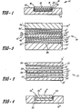
- a semiconductor die attach system 10 for attaching a semiconductor die 12 to a metal or metal-ceramic substrate 14 is illustrated in Figure 1.
- Structure 16 is disposed between the substrate 14 and the die 12 for dissipating thermal stress caused by thermal cycling.
- Seal components 18, 19 attach the thermal stress dissipating structure to both the metallic substrate 14 and the semiconductor die 12.
- the present invention is primarily directed to forming a semiconductor package wherein the substrate or base is formed of a metal having a relatively high coefficient of thermal expansion (CTE) in the area of about 170 x 10-7 in/in/°C.
- the semiconductor die which is to be attached to the substrate typically has a much lower coefficient of thermal expansion of about 50 x 10 in/in/°C.
- the semiconductor die is usually attached to the base by a gold-silicon alloy at about 400°C or a solder at about 300°C.
- the semiconductor die may be attached to the substrate with a sealing or bonding material of an alloy formed of from about 20 to about 40 wt. % silver and about 80 to about 60 wt. % tin.
- the composition of the sealing material would be about 25 to about 35 wt. % silver and about 75 to about 65 wt. % tin.
- the sealing material would be used at a temperature range of about 350°C to about 450°C and preferably at about 390°C to about 410°C.
- Another bonding material consists essentially of about 5 to about 20 wt. % copper and the balance essentially indium.
- the composition of this alloy consists essentially of about 5 to about 13 wt. % copper and the balance essentially indium.
- Still another bonding material consists essentially of about 2 to about 20 wt. % tin and the balance essentially lead.
- the composition consists essentially of about 4 to about 8 wt. % tin and the balance essentially lead.
- the surface of the die to which it is attached requires an oxidation resistant layer, as described below, because the silver-tin or other bonding materials do not wet the silicon or other typical materials of which the die is formed. In either case, die fracture typically occurs on cooling to room temperature because of the large mismatch in the coefficients of thermal expansion between the base and the die.
- the present invention overcomes this problem by inserting a thin metallic or non-metallic buffer component between the substrate and the die.
- the buffer dissipates the thermal stresses caused by the strains which are created as the die and substrate are cooled down to room temperature.
- the buffer preferably has a coefficient of thermal expansion which is much closer to the die than to the substrate. Then, as the die attach system begins to cool down, the strains caused by the mismatch in coefficients of thermal expansion occur between the buffer and the substrate instead of between the buffer and the die where the coefficients of thermal expansion are more closely matched.
- the advantage to locating the larger differential in coefficients of thermal expansion between the metal buffer and the metal substrate is that the metal to metal bond at the buffer-substrate interface is typically ductile and better able to withstand stresses and deformation.
- the component for dissipating thermal stress preferably comprises a thin, buffer component 20 of a controlled-expansion alloy having a thickness of about 1 to about 20 mils.
- the thickness of the buffer is between about 2 to about 8 mils. It is important that the buffer is relatively thin because it is designed to provide a path of stress relaxation between the semiconductor device 12 and the substrate 14. Since both the semiconductor device and the substrate 14 are relatively thick and rigid, it is important that the buffer component 20 be relatively thin in order that it provide the flexibility and deformation necessary to carrying out its stress relaxation function. In fact, the buffer component may deform into the plastic region to compensate for the strains generated during the cooling period after die attachment. However, even radical deformation of this nature does not significantly effect the operation of the semiconductor device as long as the latter neither cracks nor separates at its interface with the buffer component.
- the buffer component also has a coefficient of thermal expansion of between about 35 x 10 -7 to about 100 x 10 -7 in/in/°C.
- the buffer component has a CTE of about 40 x 10 -7 to about 80 x 10 -7 in/in/°C.
- the coefficient of thermal expansion of the buffer component be compatible and relatively close to the CTE of the semiconductor die.
- the buffer component may be constructed of a metal or alloy or ceramic having a low CTE selected from the group consisting of tungsten, rhenium, molybdenum, alloys thereof, and nickel-iron alloys and ceramics.
- nickel-iron alloys include 42 Ni-58 Fe, 64 Fe-36 Ni and 54 Fe-28Ni-18 Co. It is also within the terms of the present invention to form the buffer component of any metal or alloy which is able to meet the requirement for a suitable coefficient of thermal expansion as set out hereinabove.
- first and second barrier layers 42 and 44 on opposing surfaces 2611 and 28" of the buffer component.
- primed, double primed and triple primed reference numerals indicate components which are substantially the same as the components identified by the same unprimed reference numerals.
- the barrier layer is typically formed of a material from the group consisting of nickel, cobalt and alloys thereof. However, it is also within the terms of present invention to form the barrier layer of any suitable metal or alloy which prevents interdiffusion between the buffer material and the oxidation resistant layer formed on the barrier layer as described directly below.
- the barrier layer also enhances the bonding of the oxidation resistant layer, described hereinbelow to the buffer or substrate.
- the barrier layer is applied by any conventional means such as electroplating to thickness of about 1.5 to about 10 microns. Preferably, the thickness of the barrier layer is about 2 to about 3 microns.
- Oxidation resistant layers 22" and 24" are formed on the barrier layers 42 and 44 respectively.
- the oxidation resistant layers are typically formed of a material selected from the group consisting of gold, silver, palladium, platinum and alloys thereof. These metals are particularly chosen for their ability to resist oxidation at the high sealing temperatures to which they will be subjected.
- they are plated onto the barrier layer at a thickness of about 1.5 to about 10 microns.
- the thickness of the oxidation resistant layer is about 2 to about 3 microns. It is within the scope of the present invention to plate an oxidation resistant layer directly onto a desired surface without an intermediate barrier layer.
- the substrate 14" may be formed of a metal or alloy but may be formed of any other material such as a ceramic or a cermet having a high coefficient of thermal expansion of more than about 140 x 10 -7 in/in/°C. Typically, the substrate material has a coefficient of thermal expansion of about 160 x 10 -7 in/in/°C.
- a barrier layer 38 is formed on the surface 34' of the substrate 14". This barrier layer is formed of materials substantially the same as those mentioned with regard to the barrier layers 42 and 44 on the buffer 20". Further, an oxidation resistant layer 30' may be formed on the barrier layer 38.
- the layer 30' is formed of the same types of materials as selected for the layers 22" and 24" on the buffer 20".
- the seal or bonding components 18, 19 is a sealing material such as an alloy having a melting point of less than about 450°C.
- the seal is an alloy selected from the group consisting of gold-silicon, gold-tin, silver-tin and silver-antimony-tin.
- the seal material is a gold-2% silicon which melts at about 363°C.
- a silver-tin alloy provides an excellent, relatively unexpensive sealing material.
- the sealing material is preferably formed of from about 20 to about 40 wt. % silver and about 80 to about 60 wt. % tin.
- the composition of the sealing material would be about 25 to about 35 wt. % silver and about 75 to about 65 wt.
- % tin This material would be used at a temperature range of about 350 to about 450°C and preferably at about 390° to about 410°C.
- An important duality of the sealing material is its ability to bond to the substrate, the buffer component and the semiconductor die. In order to enhance this bonding, each of the components typically has a oxidation resistant layer as mentioned hereinabove.
- the semiconductor die 12 is typically formed of a material from the group consisting of silicon, gallium arsenide, silicon carbide and combinations thereof.
- an oxidation resistant layer may be disposed on the surface of the die. This layer is selected of any of the materials which are used to form the oxidation resistant layer on the buffer component. Preferably, this material would be the same as the other oxidation resistant layers used throughout the die attach system.
- the substrate 14" and buffer 20 preferably have a barrier layer and a oxidation resistant layer formed on their surfaces by any desired process, such as electroplating.
- the die 12" typically has an oxidation resistant layer 32' on the surface which is to be bonded.
- the base 14" is first heated on a stage to a temperature of about 365° to about 400°C. This occurs in an inert or reducing atmosphere to prevent oxidation of the substrate.
- the reducing atmosphere is commonly nitrogen-4% hydrogen while the inert atmosphere is typically either nitrogen, argon, helium or neon. However, it is also within the terms of the present invention to form these types of atmospheres with other conventional gasses.
- a strip of the seal component 18 preferably the size of the die 12" is disposed on the surface of the oxidation resistant layer 30'.
- the buffer structure 16' is stacked onto the material 18".
- a strip of material 19" essentially the same size as that disposed between the substrate and buffer component is disposed on top of the buffer component.
- the semiconductor die is placed on the seal component 19" so that its oxidation resistant layer 32' is in contact with that seal component 19".
- the entire assembly is heated until the seal component melts and bonds the entire structure together.
- the semiconductor die is moved or scrubbed on the seal component 19" to ensure proper wetting of the layer 32' so that the die is securely bond to the buffer.
- the sealed assembly is removed from the heat and cooled to room temperature. Standard interconnection techniques may be applied as required to connect the semiconductor die to a lead frame.
- the invention preferably includes a sealing component 18 between the substrate and the buffer 20, it is also within the terms of the present invention to eliminate the sealing component 18 and spot weld the buffer directly to the substrate 14. This may be accomplished by applying heat and pressure for the necessary time to achieve a degree of melting sufficient to attain solid state diffusion to bond the buffer directly to the substrate. This may further be accomplished without a barrier layer between these components. An embodiment of this scope would be illustrated in Figure 1 without the bonding layer 19.
- the component 16 for dissipating thermal stress preferably comprises a thin buffer 20 of a controlled-expansion alloy as described previously in the specification.
- the bonding or sealing components 18, 19 are selected from a bonding material such as an alloy having a melting point of less than about 450°C.
- the alloy bonding material may be selected from the group consisting of gold-silicon, gold-tin, silver-tin, silver-antimony-tin and mixtures thereof, it is a silver-tin alloy.
- the silver-tin alloy bonding material preferably consists essentially of about 20 to about 40 wt. % silver and the balance essentially tin. More preferably, the composition of this bonding material alloy consists essentially of about 25 to about 35 wt. % silver and the balance essentially tin.
- the bonding material is applied in a temperature range of about 350° to about 450°C and preferably in a range of about 390° to about 410°C.
- An important quality of the bonding material is its ability to adhere to the substrate, the buffer component and the semiconductor die.
- each of the components may, if desired, have an oxidation resistant layer or coating as described herein.
- the substrate 14 is preferably formed of a metal or alloy but may be formed of any other material such as a ceramic or a cermet having a high coefficient of thermal expansion of more than about 140 x 10-7 in/in/°C. Typically, the substrate material has a coefficient of thermal expansion of about 160 x 10 -7 in/in/°C.
- the substrate is preferably provided with a cavity 45 to receive a die 12. However, it is within the terms of the present invention to delete the cavity and attach the die onto the upper surface 47 of the substrate.
- a semiconductor die attach system 21 with first and second oxidation resistant layers 22 and 24 provided on the opposite surfaces 26 and 28 of the buffer component 20'.
- oxidation resistant layers 30 and 32 are provided on surfaces 34 and 36 of the substrate 14' and chip 12', respectively.
- the oxidation resistant layers enhance the strength of the bond between the bonding material 18' and 19' and the buffer component, the substrate and the chip.
- These layers or coatings are typically formed of a material selected from the group consisting of gold, silver, palladium, platinum and alloys thereof. It is also within the scope of the present invention to plate an oxidation resistant layer directly onto an intermediate barrier layer provided on the surface of the components as described herein.
- a fourth oxidation resistant layer 32 may be coated on the surface 36 of the die.
- This layer is preferably selected from the materials which are used to form the oxidation resistant layers on the buffer component 20'. Typically, this material would be the same as the other oxidation resistant layers used throughout the die attach system.
- the semiconductor die attach system 40 with first and second barrier layers 42 and 44 on opposing surfaces 26" and 28" of the buffer component 20".
- the barrier layer has been found to be particularly useful to prevent the formation of oxides on the surface to which it is applied.
- a barrier layer on opposite bonding surfaces of a nickel-iron buffer component prevents the formation of iron oxides on the surface of the component. These oxides could inhibit the bonding strength of the bonding material to the buffer component.
- the barrier layer may be used in conjunction with the oxidation resistant coating because the latter may not prevent oxygen from passing therethrough. For example, if silver alone were used to plate the buffer component 20", under certain bonding conditions, it would not be a strong hinderance to the interaction of oxygen with the buffer component.
- the result would be the formation of oxides, such as iron oxide which could leak through the oxidation resistant layers 22",24" and weaken the bond within the bonding material 18",19".
- the barrier layer 38 may also be coated on the surface 34' of substrate 14". It is further within the terms of the invention to selectively provide the barrier layer on any surface as desired.
- the buffer component is deleted and the semiconductor die 12"' is bonded to the substrate 14"' with only a bonding material 50.
- the preferred bonding material 50 is a silver-tin alloy having a composition which consists essentially of about 20 to about 40 wt. % silver and the balance essentially tin.
- the composition of the alloy bonding material consists essentially of about 25 to about 35 wt. % silver and the balance essentially tin.
- the silver-tin alloy is preferably free of antimony. However, it may have up to but not including 10% antimony as long as the silver-tin alloy is compliant enough for the die attachment to withstand thermal shock testing.
- the bonding material is processed in a temperature range of about 350°C to about 450°C and most preferably in a range of about 390°C to about 4l0°C.
- the die attach surface 36" is preferably coated with an oxidation resistant layer 32" because the silver-tin does not easily wet the silicon or other materials of which the die is typically formed.
- An important aspect of this invention is to provide a thick enough layer of the bonding material 50 to dissipate thermal stresses generated by the mismatch in the coefficients of thermal expansion of the die and the substrate.
- the thickness of the bonding layer is preferably between about 1 to about 15 mils.
Abstract
Description
- While the invention is subject to a wide range of applications, it is particularly suited for semiconductor die attachment and will be particularly described in that connection. More specifically, a metallic buffer component is disposed between a metallic substrate. and a semiconductor die to dissipate thermal or mechanical stresses caused by thermal exposure.
- Semiconductor dies are typically attached to hermetically sealed packages with a bonding composition of various metals or polymers. These bonding compositions usually melt at a relatively high temperature in order that they can withstand the processing temperatures required to hermetically seal a package, i.e. above 400°C. Typical bonding materials and techniques are disclosed in articles entitled "Die Bonding & Packaging Sealing Materials", by Singer in Semiconductor International, December 1983 and "A New Metal System for Die Attachment" by Winder et al. in Proc. Tech. Program - Annu. Int., Electron. Packag. Conf. 2ND, 1982, pages 715-727. Also U.S. Patent No. 3,593,412 discloses a unique attachment system.
- In a typical assembly operation, a semiconductor die or integrated circuit is placed in a cavity of a base member containing the bonding composition. The base is then heated to melt the bonding composition and adhere the die within the cavity of the base. Subsequently, the cavity is covered with a lid and heat is again applied to seal the lid to the base and form an hermetic enclosure for the die. Lid sealing temperatures are typically about 400°C to about 450°C. Examples of this type of process are disclosed in U.S. Patent Nos. 4,229,758 and 4,487,638.
- When the base and lids of the hermetically sealed semiconductor packages are formed of metal, such as selected copper alloys, the semiconductor die, typically silicon, is directly attached to the metallic substrate. Unlike the low degree of mismatch between coefficients of thermal expansion (CTE) of the components and the die which is common to the conventional ceramic packages, there is a very large mismatch betwen the coefficients of thermal expansion of the silicon and the metallic substrates, ie. about 100 to about 130 x 10-7 in/in/°C. By contrast, the mismatch in coefficients of thermal expansion of alumina and silicon is only about 15 x 10-7 in/in/°C.
- The mismatch of CTE results in the formation of large strains and resulting thermal stresses during thermal cycling. For example, when a silicon die is attached to a metal substrate with a conventional gold-2% silicon sealing metal, it is processed at a temperature of about 400°C. After the die is attached to the substrate, they are cooled down to room temperature. Very often, thermal stress caused by the large mismatch in their CTE causes the die to either crack or separate at the interface from the substrate.
- The problem from a large mismatch in CTE was demonstrated in a number of experiments where a silver backed, silicon die was directly attached to a gold plated, copper alloy substrate having a coefficient of thermal expansion of about 170 x 10-7 in/in/°C. The sealing or bonding materials were either conventional gold-2% silicon die attach alloys or a solder comprised of about 25% silver, 10% antimony and the balance tin. Using the gold-2% silicon, attachment of the silver backed, silicon die to the copper alloy substrate was unsuccessful because the die typically fractured on cooling to room temperature because of the large mismatch in the coefficients of thermal expansion between the die and the copper base alloy, i.e. about 120 x 10-7 in/in/°C.
- By contrast, die attachment with the more compliant solder was successful. However, the die did start to fracture after five cycles of thermal shock testing wherein the device was heated from room temperature to 150°C in a liquid and subsequently cooled to -65°C in a liquid. The die attach must withstand this type of thermal shock testing for at least 15 cycles to meet MIL-STD-883B, method 1011.3, condition C.
- It is a problem underlying the present invention to provide a semiconductor die attachment system for attaching a semiconductor die to a substrate which is able to withstand the stresses resulting from thermal cycling of the die and substrate.
- It is an advantage of the present invention to provide a semiconductor die attach system and process of attaching the system which obviates one or more of the limitations and disadvantages of the described prior arrangements.-It is a further advantage of the present invention to provide a semiconductor die attach system and process of attaching the system which is able to dissipate thermal stresses formed between a semiconductor die and a substrate.
- It is a yet further advantage of the present invention to provide a semiconductor die attach system and process of attaching the system wherein a buffer component disposed between a semiconductor die and a substrate provides a stress relaxation path to dissipate thermal stresses.
- It is another advantage of the present invention to provide a semiconductor die attach system and process of attaching the system wherein the buffer component is a silver-tin alloy.
- It is still another advantage of the present invention to provide a semiconductor die atttach system and process of attaching the system wherein the buffer component is a nickel-iron strip bonded with a silver-tin alloy.
- Accordingly, there has been provided a semiconductor die attach system and process of attaching the system adapted for attaching a semiconductor die to a metal or metal-ceramic substrate. In one embodiment, a metallic buffer component for dissipating thermal stresses is disposed between the substrate and the semiconductor die to dissipate stresses created by thermal cycling of the substrate and the die. The metallic component is preferably sealed between the substrate and the die with a silver-tin sealing composition. In another embodiment, a silver-tin sealing composition may be used alone to bond a die to a substrate and dissipate stresses from thermal cycling.
- The invention and further developments of the invention are now elucidated by means of the preferred embodiments in the drawings.
-
- Figure 1 illustrates a semiconductor die attach system including a buffer layer in accordance with the present invention.
- Figure 2 illustrates a semiconductor die attach system incorporating oxidation resistant layers and a buffer layer.
- Figure 3 illustrates a semiconductor die attach system incorporating a buffer layer, barrier layers and oxidation resistant layers.
- Figure 4 illustrates a semiconductor die attach system with a silver-tin solder for attaching a die to a substrate.
- A semiconductor
die attach system 10 for attaching a semiconductor die 12 to a metal or metal-ceramic substrate 14 is illustrated in Figure 1.Structure 16 is disposed between thesubstrate 14 and the die 12 for dissipating thermal stress caused by thermal cycling.Seal components metallic substrate 14 and the semiconductor die 12. - The present invention is primarily directed to forming a semiconductor package wherein the substrate or base is formed of a metal having a relatively high coefficient of thermal expansion (CTE) in the area of about 170 x 10-7 in/in/°C. The semiconductor die which is to be attached to the substrate typically has a much lower coefficient of thermal expansion of about 50 x 10 in/in/°C.The semiconductor die is usually attached to the base by a gold-silicon alloy at about 400°C or a solder at about 300°C. However, it has been found that the semiconductor die may be attached to the substrate with a sealing or bonding material of an alloy formed of from about 20 to about 40 wt. % silver and about 80 to about 60 wt. % tin. Preferably, the composition of the sealing material would be about 25 to about 35 wt. % silver and about 75 to about 65 wt. % tin. The sealing material would be used at a temperature range of about 350°C to about 450°C and preferably at about 390°C to about 410°C.
- Another bonding material consists essentially of about 5 to about 20 wt. % copper and the balance essentially indium. Preferably, the composition of this alloy consists essentially of about 5 to about 13 wt. % copper and the balance essentially indium. Still another bonding material consists essentially of about 2 to about 20 wt. % tin and the balance essentially lead. Preferably, the composition consists essentially of about 4 to about 8 wt. % tin and the balance essentially lead.
- With a silver-tin sealing material and with the other bonding materials, the surface of the die to which it is attached requires an oxidation resistant layer, as described below, because the silver-tin or other bonding materials do not wet the silicon or other typical materials of which the die is formed. In either case, die fracture typically occurs on cooling to room temperature because of the large mismatch in the coefficients of thermal expansion between the base and the die.
- The present invention overcomes this problem by inserting a thin metallic or non-metallic buffer component between the substrate and the die. The buffer dissipates the thermal stresses caused by the strains which are created as the die and substrate are cooled down to room temperature. The buffer preferably has a coefficient of thermal expansion which is much closer to the die than to the substrate. Then, as the die attach system begins to cool down, the strains caused by the mismatch in coefficients of thermal expansion occur between the buffer and the substrate instead of between the buffer and the die where the coefficients of thermal expansion are more closely matched. The advantage to locating the larger differential in coefficients of thermal expansion between the metal buffer and the metal substrate is that the metal to metal bond at the buffer-substrate interface is typically ductile and better able to withstand stresses and deformation. On the other hand, it is important to reduce stresses and deformation at the interface of the buffer and the die because the semiconductor material is very brittle and not able to withstand any significant deformation. In fact, any stresses between the brittle semiconductor material and the metal buffer is likely to cause cracking of the semiconductor material or separation at the die-substrate interface.
- Referring to Figure 1, the component for dissipating thermal stress preferably comprises a thin,
buffer component 20 of a controlled-expansion alloy having a thickness of about 1 to about 20 mils. Preferably, the thickness of the buffer is between about 2 to about 8 mils. It is important that the buffer is relatively thin because it is designed to provide a path of stress relaxation between thesemiconductor device 12 and thesubstrate 14. Since both the semiconductor device and thesubstrate 14 are relatively thick and rigid, it is important that thebuffer component 20 be relatively thin in order that it provide the flexibility and deformation necessary to carrying out its stress relaxation function. In fact, the buffer component may deform into the plastic region to compensate for the strains generated during the cooling period after die attachment. However, even radical deformation of this nature does not significantly effect the operation of the semiconductor device as long as the latter neither cracks nor separates at its interface with the buffer component. - The buffer component also has a coefficient of thermal expansion of between about 35 x 10-7 to about 100 x 10-7 in/in/°C. Preferably, the buffer component has a CTE of about 40 x 10-7 to about 80 x 10-7 in/in/°C. In general, it is desirable that the coefficient of thermal expansion of the buffer component be compatible and relatively close to the CTE of the semiconductor die. The buffer component may be constructed of a metal or alloy or ceramic having a low CTE selected from the group consisting of tungsten, rhenium, molybdenum, alloys thereof, and nickel-iron alloys and ceramics. Several examples of particular nickel-iron alloys include 42 Ni-58 Fe, 64 Fe-36 Ni and 54 Fe-28Ni-18 Co. It is also within the terms of the present invention to form the buffer component of any metal or alloy which is able to meet the requirement for a suitable coefficient of thermal expansion as set out hereinabove.
- As illustrated in Figure 3, in order for the material of the buffer component 2011 to form a strong seal with the seal or
bonding components 18", 19", it is often necessary to form first and second barrier layers 42 and 44 on opposingsurfaces 2611 and 28" of the buffer component. Throughout the specification, primed, double primed and triple primed reference numerals indicate components which are substantially the same as the components identified by the same unprimed reference numerals. The barrier layer is typically formed of a material from the group consisting of nickel, cobalt and alloys thereof. However, it is also within the terms of present invention to form the barrier layer of any suitable metal or alloy which prevents interdiffusion between the buffer material and the oxidation resistant layer formed on the barrier layer as described directly below. The barrier layer also enhances the bonding of the oxidation resistant layer, described hereinbelow to the buffer or substrate. The barrier layer is applied by any conventional means such as electroplating to thickness of about 1.5 to about 10 microns. Preferably, the thickness of the barrier layer is about 2 to about 3 microns. - Oxidation
resistant layers 22" and 24" are formed on the barrier layers 42 and 44 respectively. The oxidation resistant layers are typically formed of a material selected from the group consisting of gold, silver, palladium, platinum and alloys thereof. These metals are particularly chosen for their ability to resist oxidation at the high sealing temperatures to which they will be subjected. Typically they are plated onto the barrier layer at a thickness of about 1.5 to about 10 microns. Preferably, the thickness of the oxidation resistant layer is about 2 to about 3 microns. It is within the scope of the present invention to plate an oxidation resistant layer directly onto a desired surface without an intermediate barrier layer. - The
substrate 14" may be formed of a metal or alloy but may be formed of any other material such as a ceramic or a cermet having a high coefficient of thermal expansion of more than about 140 x 10-7 in/in/°C. Typically, the substrate material has a coefficient of thermal expansion of about 160 x 10-7 in/in/°C. As with thebuffer 20", it is desirable to form abarrier layer 38 on the surface 34' of thesubstrate 14". This barrier layer is formed of materials substantially the same as those mentioned with regard to the barrier layers 42 and 44 on thebuffer 20". Further, an oxidation resistant layer 30' may be formed on thebarrier layer 38. The layer 30' is formed of the same types of materials as selected for thelayers 22" and 24" on thebuffer 20". - The seal or
bonding components - The semiconductor die 12 is typically formed of a material from the group consisting of silicon, gallium arsenide, silicon carbide and combinations thereof. In order for the die 12 to be sealed to seal
component 19, an oxidation resistant layer may be disposed on the surface of the die. This layer is selected of any of the materials which are used to form the oxidation resistant layer on the buffer component. Preferably, this material would be the same as the other oxidation resistant layers used throughout the die attach system. - To further understand the present invention, an explanation of the process by which the semiconductor die is attached to the buffer component 16' and metal substrate is provided herein with reference to Figure 3. The
substrate 14" andbuffer 20", preferably have a barrier layer and a oxidation resistant layer formed on their surfaces by any desired process, such as electroplating. The die 12" typically has an oxidation resistant layer 32' on the surface which is to be bonded. The base 14" is first heated on a stage to a temperature of about 365° to about 400°C. This occurs in an inert or reducing atmosphere to prevent oxidation of the substrate. The reducing atmosphere is commonly nitrogen-4% hydrogen while the inert atmosphere is typically either nitrogen, argon, helium or neon. However, it is also within the terms of the present invention to form these types of atmospheres with other conventional gasses. - Once the substrate has been heated to the desired temperature, a strip of the
seal component 18", preferably the size of the die 12" is disposed on the surface of the oxidation resistant layer 30'. Then the buffer structure 16' is stacked onto the material 18". Then a strip ofmaterial 19" essentially the same size as that disposed between the substrate and buffer component is disposed on top of the buffer component. Finally, the semiconductor die is placed on theseal component 19" so that its oxidation resistant layer 32' is in contact with thatseal component 19". The entire assembly is heated until the seal component melts and bonds the entire structure together. Typically, the semiconductor die is moved or scrubbed on theseal component 19" to ensure proper wetting of the layer 32' so that the die is securely bond to the buffer. Finally, the sealed assembly is removed from the heat and cooled to room temperature. Standard interconnection techniques may be applied as required to connect the semiconductor die to a lead frame. - Although the invention preferably includes a
sealing component 18 between the substrate and thebuffer 20, it is also within the terms of the present invention to eliminate thesealing component 18 and spot weld the buffer directly to thesubstrate 14. This may be accomplished by applying heat and pressure for the necessary time to achieve a degree of melting sufficient to attain solid state diffusion to bond the buffer directly to the substrate. This may further be accomplished without a barrier layer between these components. An embodiment of this scope would be illustrated in Figure 1 without thebonding layer 19. - Referring to the embodiment as shown in Figure 1, a basic die attach
system 10 embodying the concepts of the present invention is set out. Thecomponent 16 for dissipating thermal stress preferably comprises athin buffer 20 of a controlled-expansion alloy as described previously in the specification. - The bonding or sealing
components - The
substrate 14 is preferably formed of a metal or alloy but may be formed of any other material such as a ceramic or a cermet having a high coefficient of thermal expansion of more than about 140 x 10-7 in/in/°C. Typically, the substrate material has a coefficient of thermal expansion of about 160 x 10-7 in/in/°C. The substrate is preferably provided with acavity 45 to receive adie 12. However, it is within the terms of the present invention to delete the cavity and attach the die onto theupper surface 47 of the substrate. - Referring to Figure 2, there is illustrated a semiconductor die attach
system 21 with first and second oxidationresistant layers opposite surfaces resistant layers surfaces - To improve the adherence of the die 12' to seal component 19', a fourth oxidation
resistant layer 32 may be coated on thesurface 36 of the die. This layer is preferably selected from the materials which are used to form the oxidation resistant layers on the buffer component 20'. Typically, this material would be the same as the other oxidation resistant layers used throughout the die attach system. - Referring to Figure 3, there is illustrated the semiconductor die attach
system 40 with first and second barrier layers 42 and 44 on opposingsurfaces 26" and 28" of thebuffer component 20". The barrier layer has been found to be particularly useful to prevent the formation of oxides on the surface to which it is applied. For example, a barrier layer on opposite bonding surfaces of a nickel-iron buffer component prevents the formation of iron oxides on the surface of the component. These oxides could inhibit the bonding strength of the bonding material to the buffer component. The barrier layer may be used in conjunction with the oxidation resistant coating because the latter may not prevent oxygen from passing therethrough. For example, if silver alone were used to plate thebuffer component 20", under certain bonding conditions, it would not be a strong hinderance to the interaction of oxygen with the buffer component. The result would be the formation of oxides, such as iron oxide which could leak through the oxidationresistant layers 22",24" and weaken the bond within thebonding material 18",19". Thebarrier layer 38 may also be coated on the surface 34' ofsubstrate 14". It is further within the terms of the invention to selectively provide the barrier layer on any surface as desired. - In another embodiment, as illustrated in Figure 4, the buffer component is deleted and the semiconductor die 12"' is bonded to the
substrate 14"' with only abonding material 50. It is now thought that the bonding material alone, if it is compliant enough to withstand thermal shock testing, can adequately dissipate thermal stress from thermal cycling. However, the buffer component is still advantageous in the system because it distributes stress over the greater thickness of buffer material, as compared to the bonding material above. Thepreferred bonding material 50 is a silver-tin alloy having a composition which consists essentially of about 20 to about 40 wt. % silver and the balance essentially tin. Preferably, the composition of the alloy bonding material consists essentially of about 25 to about 35 wt. % silver and the balance essentially tin. The silver-tin alloy is preferably free of antimony. However, it may have up to but not including 10% antimony as long as the silver-tin alloy is compliant enough for the die attachment to withstand thermal shock testing. - Preferably, the bonding material is processed in a temperature range of about 350°C to about 450°C and most preferably in a range of about 390°C to about 4l0°C. With a silver-tin bonding material, the die attach
surface 36" is preferably coated with an oxidationresistant layer 32" because the silver-tin does not easily wet the silicon or other materials of which the die is typically formed. An important aspect of this invention is to provide a thick enough layer of thebonding material 50 to dissipate thermal stresses generated by the mismatch in the coefficients of thermal expansion of the die and the substrate. The thickness of the bonding layer is preferably between about 1 to about 15 mils. - In order for the bonding component to satisfactorily bond to the
substrate 14"', it may be desirable tocoat surface 52 with an oxidation resistant layer of material as described above in the specification. Further, a buffer layer of the material described in the embodiment illustrated in Figure 3 may be disposed between the -oxidation layer and the substrate surface if desired. Embodiments within this scope are illustrated in Figures 2 and 3 after the removal of thebuffer 20' or 20". - It is apparent that there has been provided in accordance with the present invention a semiconductor die attach system and process of using the system which fully satisfies the objects, means and advantages set forth hereinabove. While the invention has been described in combination with the embodiments thereof, it is evident that many alternatives, modifications and variations will be apparent to those skilled in the art in light of the foregoing description. Accordingly, it is intended to embrace all such alternatives, modifications and variations as fall within the spirit and broad scope of the appended claims.
Claims (20)
Applications Claiming Priority (6)
| Application Number | Priority Date | Filing Date | Title |
|---|---|---|---|
| US71186885A | 1985-03-14 | 1985-03-14 | |
| US711868 | 1985-03-14 | ||
| US740789 | 1985-06-03 | ||
| US74078985A | 1985-06-08 | 1985-06-08 | |
| US826808 | 1986-02-10 | ||
| US06/826,808 US4929516A (en) | 1985-03-14 | 1986-02-10 | Semiconductor die attach system |
Publications (2)
| Publication Number | Publication Date |
|---|---|
| EP0194475A2 true EP0194475A2 (en) | 1986-09-17 |
| EP0194475A3 EP0194475A3 (en) | 1988-04-20 |
Family
ID=27418893
Family Applications (1)
| Application Number | Title | Priority Date | Filing Date |
|---|---|---|---|
| EP86102059A Withdrawn EP0194475A3 (en) | 1985-03-14 | 1986-02-18 | Semiconductor die attach system |
Country Status (6)
| Country | Link |
|---|---|
| US (1) | US4929516A (en) |
| EP (1) | EP0194475A3 (en) |
| KR (1) | KR860007734A (en) |
| CN (1) | CN86101652A (en) |
| CA (1) | CA1249669A (en) |
| MX (1) | MX164788B (en) |
Cited By (17)
| Publication number | Priority date | Publication date | Assignee | Title |
|---|---|---|---|---|
| US4872047A (en) * | 1986-11-07 | 1989-10-03 | Olin Corporation | Semiconductor die attach system |
| US4978052A (en) * | 1986-11-07 | 1990-12-18 | Olin Corporation | Semiconductor die attach system |
| EP0416847A2 (en) * | 1989-09-06 | 1991-03-13 | Plessey Semiconductors Limited | Methods of joining components |
| EP0467259A2 (en) * | 1990-07-18 | 1992-01-22 | Hitachi, Ltd. | Electronic device |
| EP0585084A1 (en) * | 1992-08-28 | 1994-03-02 | AT&T Corp. | Permanent metallic bonding method |
| EP0618619A1 (en) * | 1993-03-29 | 1994-10-05 | Delco Electronics Corporation | Ultra-thick thick films for thermal management and current-carrying capabilities in hybrid circuits |
| EP0622837A1 (en) * | 1993-04-27 | 1994-11-02 | Nec Corporation | An optical semiconductor device and a method of manufacturing the same |
| WO1994027319A1 (en) * | 1993-05-07 | 1994-11-24 | Siemens Aktiengesellschaft | Power semiconductor device with stress buffer layer |
| EP0696063A3 (en) * | 1994-07-25 | 1996-08-07 | Gen Electric | Thermally conductive material |
| DE10111185A1 (en) * | 2001-03-08 | 2002-06-13 | Siemens Ag | Ceramic-metal substrate has profiling in metal layer for reducing thermodynamic stresses provided in vicinity of electrical components or contact elements |
| WO2002056376A2 (en) * | 2000-11-17 | 2002-07-18 | Sun Microsystems, Inc. | Method of integrating a heat spreader and a semiconductor, and package formed thereby |
| WO2004051733A1 (en) * | 2002-11-27 | 2004-06-17 | Freescale Semiconductor, Inc. | Thin gaas die with copper back-metal structure |
| US9157669B2 (en) | 2011-04-20 | 2015-10-13 | Empire Technology Development Llc | Heterogeneous electrocaloric effect heat transfer device |
| US9310109B2 (en) | 2011-09-21 | 2016-04-12 | Empire Technology Development Llc | Electrocaloric effect heat transfer device dimensional stress control |
| US9318192B2 (en) | 2012-09-18 | 2016-04-19 | Empire Technology Development Llc | Phase change memory thermal management with electrocaloric effect materials |
| US9500392B2 (en) | 2012-07-17 | 2016-11-22 | Empire Technology Development Llc | Multistage thermal flow device and thermal energy transfer |
| US9671140B2 (en) | 2011-09-21 | 2017-06-06 | Empire Technology Development Llc | Heterogeneous electrocaloric effect heat transfer |
Families Citing this family (22)
| Publication number | Priority date | Publication date | Assignee | Title |
|---|---|---|---|---|
| JPH0349834A (en) * | 1989-07-14 | 1991-03-04 | Sumitomo Electric Ind Ltd | Tool using gold as sealant and manufacture thereof |
| US5292559A (en) * | 1992-01-10 | 1994-03-08 | Amp Incorporated | Laser transfer process |
| US5369403A (en) * | 1992-09-01 | 1994-11-29 | The State Of Oregon Acting By And Through The State Board Of Higher Education On Behalf Of Oregon State University | Dual quantization oversampling digital-to-analog converter |
| US5559817A (en) * | 1994-11-23 | 1996-09-24 | Lucent Technologies Inc. | Complaint layer metallization |
| JPH09275182A (en) * | 1996-04-02 | 1997-10-21 | Seiichi Serizawa | Lead frame for semiconductor device |
| US6179943B1 (en) * | 1997-07-30 | 2001-01-30 | The Boeing Company | Method for forming a composite acoustic panel |
| US6642078B2 (en) * | 2000-08-28 | 2003-11-04 | Transpo Electronics, Inc. | Method for manufacturing diode subassemblies used in rectifier assemblies of engine driven generators |
| EP1320889A1 (en) * | 2000-09-29 | 2003-06-25 | Infineon Technologies AG | Connecting device |
| DE10221857A1 (en) * | 2002-05-16 | 2003-11-27 | Osram Opto Semiconductors Gmbh | Process for applying a semiconductor chip on a thermal and/or electrically conducting connecting part arranged in or on a plastic housing body comprises using a soft soldering process |
| US7164585B2 (en) * | 2003-03-31 | 2007-01-16 | Intel Corporation | Thermal interface apparatus, systems, and methods |
| DE102004001956B4 (en) * | 2004-01-13 | 2007-02-01 | Infineon Technologies Ag | Redistributable substrate strip with multiple semiconductor device locations |
| JP3994980B2 (en) * | 2004-03-29 | 2007-10-24 | 株式会社日立製作所 | Device mounting substrate, manufacturing method thereof, and semiconductor device mounting method |
| JP4343117B2 (en) * | 2005-01-07 | 2009-10-14 | 株式会社ルネサステクノロジ | Semiconductor device and manufacturing method thereof |
| DE602005015103D1 (en) * | 2005-07-28 | 2009-08-06 | Infineon Technologies Ag | A connection structure for mounting a semiconductor chip on a metal substrate, semiconductor chip, and electronic device having the connection structure, and methods of manufacturing the connection structure |
| DE102005051811A1 (en) * | 2005-10-27 | 2007-05-03 | Infineon Technologies Ag | Semiconductor component with semiconductor chip in surface conductive frame technology has chip carrier on chip connection surface with metallic buffer layer and cover layer |
| US8283756B2 (en) * | 2007-08-20 | 2012-10-09 | Infineon Technologies Ag | Electronic component with buffer layer |
| EP2583320A4 (en) | 2010-06-18 | 2014-01-22 | Empire Technology Dev Llc | Electrocaloric effect materials and thermal diodes |
| JP5988977B2 (en) * | 2011-07-28 | 2016-09-07 | デンカ株式会社 | Heat dissipation parts for semiconductor elements |
| CN103814259B (en) * | 2011-09-21 | 2015-12-16 | 英派尔科技开发有限公司 | Electrocaloric effect heat-transfer arrangement size Stress Control |
| KR102311677B1 (en) * | 2014-08-13 | 2021-10-12 | 삼성전자주식회사 | Semiconductor device and method of manufacturing the same |
| CN106169448A (en) * | 2016-07-26 | 2016-11-30 | 昆山华太电子技术有限公司 | A kind of power device package of high heat conduction |
| CN109727924B (en) * | 2018-12-27 | 2020-07-17 | 江苏省宜兴电子器件总厂有限公司 | Ceramic shell packaging structure with AlN and Si transition piece |
Citations (3)
| Publication number | Priority date | Publication date | Assignee | Title |
|---|---|---|---|---|
| CH391108A (en) * | 1960-06-28 | 1965-04-30 | Siemens Ag | Method for producing the electrical connections of a semiconductor arrangement |
| EP0070435A2 (en) * | 1981-07-02 | 1983-01-26 | Matsushita Electronics Corporation | Semiconductor device comprising a semiconductor substrate bonded to a mounting means |
| WO1983000949A1 (en) * | 1981-09-01 | 1983-03-17 | Motorola Inc | Improved glass bonding means and method |
Family Cites Families (34)
| Publication number | Priority date | Publication date | Assignee | Title |
|---|---|---|---|---|
| CA707458A (en) * | 1965-04-06 | The Nippert Electric Products Company | Mounts for semiconductors and method of making same | |
| CA904567A (en) * | 1972-07-11 | Westinghouse Electric Corporation | Low thermal expansion binder | |
| CA676283A (en) * | 1963-12-17 | Siemens Alfred | Electric semiconductor device | |
| CA755785A (en) * | 1967-03-28 | L. Davies Robert | Semiconductor device | |
| CA700474A (en) * | 1964-12-22 | Siemens-Schuckertwerke Aktiengesellschaft | Method of producing electrically asymmetrical semiconductor devices, and products of such methods | |
| CA667024A (en) * | 1963-07-16 | Siemens-Schuckertwerke Aktiengesellschaft | Semiconductor device | |
| NL107577C (en) * | 1954-07-01 | |||
| US2763822A (en) * | 1955-05-10 | 1956-09-18 | Westinghouse Electric Corp | Silicon semiconductor devices |
| US2922092A (en) * | 1957-05-09 | 1960-01-19 | Westinghouse Electric Corp | Base contact members for semiconductor devices |
| BE577086A (en) * | 1958-04-03 | 1900-01-01 | ||
| US3160798A (en) * | 1959-12-07 | 1964-12-08 | Gen Electric | Semiconductor devices including means for securing the elements |
| NL291270A (en) * | 1961-08-12 | |||
| US3159462A (en) * | 1962-09-24 | 1964-12-01 | Int Rectifier Corp | Semiconductor and secured metal base and method of making the same |
| US3454374A (en) * | 1966-05-13 | 1969-07-08 | Youngwood Electronic Metals In | Method of forming presoldering components and composite presoldering components made thereby |
| US3503721A (en) * | 1967-02-16 | 1970-03-31 | Nytronics Inc | Electronic components joined by tinsilver eutectic solder |
| JPS4810904B1 (en) * | 1969-03-12 | 1973-04-09 | ||
| US3593412A (en) * | 1969-07-22 | 1971-07-20 | Motorola Inc | Bonding system for semiconductor device |
| US3645785A (en) * | 1969-11-12 | 1972-02-29 | Texas Instruments Inc | Ohmic contact system |
| US3620692A (en) * | 1970-04-01 | 1971-11-16 | Rca Corp | Mounting structure for high-power semiconductor devices |
| US3859715A (en) * | 1970-12-21 | 1975-01-14 | Signetics Corp | System and method for attaching semiconductor dice to leads |
| JPS5422163A (en) * | 1977-07-21 | 1979-02-19 | Toshiba Corp | Semiconductor device |
| JPS598358Y2 (en) * | 1978-02-08 | 1984-03-15 | 京セラ株式会社 | Semiconductor element package |
| JPS5850421B2 (en) * | 1978-07-19 | 1983-11-10 | 株式会社東芝 | thin film circuit |
| JPS56114338A (en) * | 1980-02-14 | 1981-09-08 | Fujitsu Ltd | Semiconductor device |
| US4515898A (en) * | 1981-09-01 | 1985-05-07 | Motorola, Inc. | Glass bonding means and method |
| US4592794A (en) * | 1981-09-01 | 1986-06-03 | Motorola, Inc. | Glass bonding method |
| JPS58151036A (en) * | 1982-03-03 | 1983-09-08 | Hitachi Ltd | Semiconductor device |
| US4656499A (en) * | 1982-08-05 | 1987-04-07 | Olin Corporation | Hermetically sealed semiconductor casing |
| US4487638A (en) * | 1982-11-24 | 1984-12-11 | Burroughs Corporation | Semiconductor die-attach technique and composition therefor |
| JPS59107527A (en) * | 1982-12-13 | 1984-06-21 | Hitachi Ltd | Semiconductor device |
| JPS59151437A (en) * | 1983-02-18 | 1984-08-29 | Hitachi Ltd | Semiconductor device and manufacture thereof |
| JPS6041234A (en) * | 1983-08-17 | 1985-03-04 | Hitachi Ltd | Semiconductor device |
| JPS60235430A (en) * | 1984-05-09 | 1985-11-22 | Hitachi Ltd | Semiconductor device |
| US4610934A (en) * | 1985-01-17 | 1986-09-09 | Kennecott Corporation | Silicon carbide-to-metal joint and method of making same |
-
1986
- 1986-02-10 US US06/826,808 patent/US4929516A/en not_active Expired - Fee Related
- 1986-02-18 EP EP86102059A patent/EP0194475A3/en not_active Withdrawn
- 1986-02-19 CA CA000502175A patent/CA1249669A/en not_active Expired
- 1986-02-26 MX MX1672A patent/MX164788B/en unknown
- 1986-03-11 KR KR1019860001713A patent/KR860007734A/en not_active Application Discontinuation
- 1986-03-14 CN CN86101652A patent/CN86101652A/en active Pending
Patent Citations (3)
| Publication number | Priority date | Publication date | Assignee | Title |
|---|---|---|---|---|
| CH391108A (en) * | 1960-06-28 | 1965-04-30 | Siemens Ag | Method for producing the electrical connections of a semiconductor arrangement |
| EP0070435A2 (en) * | 1981-07-02 | 1983-01-26 | Matsushita Electronics Corporation | Semiconductor device comprising a semiconductor substrate bonded to a mounting means |
| WO1983000949A1 (en) * | 1981-09-01 | 1983-03-17 | Motorola Inc | Improved glass bonding means and method |
Non-Patent Citations (6)
| Title |
|---|
| PATENT ABSTRACTS OF JAPAN, Vol. 10, No. 91 (E-394)(2148), 9th April 1986; & JP-A-60 235 430 (HITACHI SEISAKUSHO K.K.) 22-11-1985 * |
| PATENT ABSTRACTS OF JAPAN, Vol. 5, No. 192 (E-85)(864), 8th December 1981; & JP-A-56 114 338 (FUJITSU K.K.) 08-09-1981 * |
| PATENT ABSTRACTS OF JAPAN, Vol. 7, No. 267 (E-213)(1412), 29th November 1983; & JP-A-58 151 036 (HITACHI SEISAKUSHO K.K.) 08-09-1983 * |
| PATENT ABSTRACTS OF JAPAN, Vol. 8, No. 226 (E-272)(1663), 17th October 1984; & JP-A-59 107 527 (HITACHI SEISAKUSHO K.K.) 21-06-1984 * |
| PATENT ABSTRACTS OF JAPAN, Vol. 8, No. 285 (E-287)(1722), 26th December 1984; & JP-A-59 151 437 (HITACHI SEISAKUSHO K.K.) 29-08-1984 * |
| PATENT ABSTRACTS OF JAPAN, Vol. 9, No. 165 (E-327)(1888), 10th July 1985; & JP-A-60 041 234 (HITACHI SEISAKUSHO K.K.) 04-03-1985 * |
Cited By (28)
| Publication number | Priority date | Publication date | Assignee | Title |
|---|---|---|---|---|
| US4978052A (en) * | 1986-11-07 | 1990-12-18 | Olin Corporation | Semiconductor die attach system |
| US4872047A (en) * | 1986-11-07 | 1989-10-03 | Olin Corporation | Semiconductor die attach system |
| EP0416847A2 (en) * | 1989-09-06 | 1991-03-13 | Plessey Semiconductors Limited | Methods of joining components |
| EP0416847A3 (en) * | 1989-09-06 | 1992-03-11 | Marconi Electronic Devices Limited | Methods of joining components |
| US5606487A (en) * | 1990-07-18 | 1997-02-25 | Hitachi, Ltd. | Electronic device for offsetting adverse effects of a plurality of chips which repetitively produce large pulses of heat |
| EP0467259A2 (en) * | 1990-07-18 | 1992-01-22 | Hitachi, Ltd. | Electronic device |
| EP0467259A3 (en) * | 1990-07-18 | 1992-05-20 | Hitachi, Ltd. | Electronic device |
| EP0585084A1 (en) * | 1992-08-28 | 1994-03-02 | AT&T Corp. | Permanent metallic bonding method |
| EP0618619A1 (en) * | 1993-03-29 | 1994-10-05 | Delco Electronics Corporation | Ultra-thick thick films for thermal management and current-carrying capabilities in hybrid circuits |
| US5854087A (en) * | 1993-04-27 | 1998-12-29 | Nec Corporation | Method of manufacturing an optical semiconductor device |
| EP0622837A1 (en) * | 1993-04-27 | 1994-11-02 | Nec Corporation | An optical semiconductor device and a method of manufacturing the same |
| US5917200A (en) * | 1993-04-27 | 1999-06-29 | Nec Corporation | Optical semiconductor device |
| WO1994027319A1 (en) * | 1993-05-07 | 1994-11-24 | Siemens Aktiengesellschaft | Power semiconductor device with stress buffer layer |
| US5654586A (en) * | 1993-05-07 | 1997-08-05 | Siemens Aktiengesellschaft | Power semiconductor component having a buffer layer |
| EP0696063A3 (en) * | 1994-07-25 | 1996-08-07 | Gen Electric | Thermally conductive material |
| US5567985A (en) * | 1994-07-25 | 1996-10-22 | General Electric Company | Electronic apparatus with compliant metal chip-substrate bonding layer(s) |
| WO2002056376A3 (en) * | 2000-11-17 | 2003-03-13 | Sun Microsystems Inc | Method of integrating a heat spreader and a semiconductor, and package formed thereby |
| WO2002056376A2 (en) * | 2000-11-17 | 2002-07-18 | Sun Microsystems, Inc. | Method of integrating a heat spreader and a semiconductor, and package formed thereby |
| US6586279B1 (en) | 2000-11-17 | 2003-07-01 | Sun Microsystems, Inc. | Method of integrating a heat spreader and a semiconductor, and package formed thereby |
| DE10111185A1 (en) * | 2001-03-08 | 2002-06-13 | Siemens Ag | Ceramic-metal substrate has profiling in metal layer for reducing thermodynamic stresses provided in vicinity of electrical components or contact elements |
| WO2004051733A1 (en) * | 2002-11-27 | 2004-06-17 | Freescale Semiconductor, Inc. | Thin gaas die with copper back-metal structure |
| US6870243B2 (en) | 2002-11-27 | 2005-03-22 | Freescale Semiconductor, Inc. | Thin GaAs die with copper back-metal structure |
| US7092890B2 (en) | 2002-11-27 | 2006-08-15 | Freescale Semiconductor, Inc. | Method for manufacturing thin GaAs die with copper-back metal structures |
| US9157669B2 (en) | 2011-04-20 | 2015-10-13 | Empire Technology Development Llc | Heterogeneous electrocaloric effect heat transfer device |
| US9310109B2 (en) | 2011-09-21 | 2016-04-12 | Empire Technology Development Llc | Electrocaloric effect heat transfer device dimensional stress control |
| US9671140B2 (en) | 2011-09-21 | 2017-06-06 | Empire Technology Development Llc | Heterogeneous electrocaloric effect heat transfer |
| US9500392B2 (en) | 2012-07-17 | 2016-11-22 | Empire Technology Development Llc | Multistage thermal flow device and thermal energy transfer |
| US9318192B2 (en) | 2012-09-18 | 2016-04-19 | Empire Technology Development Llc | Phase change memory thermal management with electrocaloric effect materials |
Also Published As
| Publication number | Publication date |
|---|---|
| CN86101652A (en) | 1986-11-12 |
| EP0194475A3 (en) | 1988-04-20 |
| KR860007734A (en) | 1986-10-17 |
| MX164788B (en) | 1992-09-24 |
| CA1249669A (en) | 1989-01-31 |
| US4929516A (en) | 1990-05-29 |
Similar Documents
| Publication | Publication Date | Title |
|---|---|---|
| US4929516A (en) | Semiconductor die attach system | |
| US4872047A (en) | Semiconductor die attach system | |
| US4784974A (en) | Method of making a hermetically sealed semiconductor casing | |
| US4656499A (en) | Hermetically sealed semiconductor casing | |
| US5001546A (en) | Clad metal lead frame substrates | |
| JP3126977B2 (en) | Reinforced direct bond copper structure | |
| US4978052A (en) | Semiconductor die attach system | |
| US4649229A (en) | All metal flat package for microcircuitry | |
| US5786548A (en) | Hermetic package for an electrical device | |
| JPS59124150A (en) | Bonding method | |
| EP0989605B1 (en) | Production method for lid material for a package for electronic components. | |
| US5105258A (en) | Metal system for semiconductor die attach | |
| US5046656A (en) | Vacuum die attach for integrated circuits | |
| EP0090566A2 (en) | Semiconductor device package | |
| JP2005032834A (en) | Joining method of semiconductor chip and substrate | |
| US6131796A (en) | Direct brazing of refractory metal features | |
| US4504849A (en) | Semiconductor devices and a solder for use in such devices | |
| EP0100817B1 (en) | A hermetically sealed casing of an electrical device and process of manufacturing | |
| JPS6153851B2 (en) | ||
| US6306526B1 (en) | Semiconductor packaging metal lid | |
| EP0264128A2 (en) | Jumper chip for semiconductor devices | |
| JP2000068396A (en) | Cover for hermetic seal | |
| US4837928A (en) | Method of producing a jumper chip for semiconductor devices | |
| JPH07105464B2 (en) | Semiconductor device for mounting semiconductor elements | |
| JPS61268032A (en) | Semiconductor die bonding apparatus |
Legal Events
| Date | Code | Title | Description |
|---|---|---|---|
| PUAI | Public reference made under article 153(3) epc to a published international application that has entered the european phase |
Free format text: ORIGINAL CODE: 0009012 |
|
| AK | Designated contracting states |
Kind code of ref document: A2 Designated state(s): BE DE FR GB IT NL SE |
|
| PUAL | Search report despatched |
Free format text: ORIGINAL CODE: 0009013 |
|
| AK | Designated contracting states |
Kind code of ref document: A3 Designated state(s): BE DE FR GB IT NL SE |
|
| 17P | Request for examination filed |
Effective date: 19881019 |
|
| 17Q | First examination report despatched |
Effective date: 19910305 |
|
| STAA | Information on the status of an ep patent application or granted ep patent |
Free format text: STATUS: THE APPLICATION IS DEEMED TO BE WITHDRAWN |
|
| 18D | Application deemed to be withdrawn |
Effective date: 19930126 |
|
| RIN1 | Information on inventor provided before grant (corrected) |
Inventor name: SINGHDEO, NARENDRA N. Inventor name: PRYOR, MICHAEL J. Inventor name: CHERUKURI, SATYAM C. Inventor name: MAHULIKAR, DEEPAK Inventor name: FISTER, JULIUS C. |