EP0192229A2 - Conductivity modulation type semiconductor device and method for manufacturing the same - Google Patents
Conductivity modulation type semiconductor device and method for manufacturing the same Download PDFInfo
- Publication number
- EP0192229A2 EP0192229A2 EP86102047A EP86102047A EP0192229A2 EP 0192229 A2 EP0192229 A2 EP 0192229A2 EP 86102047 A EP86102047 A EP 86102047A EP 86102047 A EP86102047 A EP 86102047A EP 0192229 A2 EP0192229 A2 EP 0192229A2
- Authority
- EP
- European Patent Office
- Prior art keywords
- region
- layer
- type
- semiconductor
- semiconductor device
- Prior art date
- Legal status (The legal status is an assumption and is not a legal conclusion. Google has not performed a legal analysis and makes no representation as to the accuracy of the status listed.)
- Granted
Links
- 239000004065 semiconductor Substances 0.000 title claims abstract description 79
- 238000000034 method Methods 0.000 title claims description 19
- 238000004519 manufacturing process Methods 0.000 title claims description 9
- 239000000758 substrate Substances 0.000 claims abstract description 60
- 210000000746 body region Anatomy 0.000 claims abstract description 24
- 239000012535 impurity Substances 0.000 claims abstract description 19
- XUIMIQQOPSSXEZ-UHFFFAOYSA-N Silicon Chemical compound [Si] XUIMIQQOPSSXEZ-UHFFFAOYSA-N 0.000 description 33
- 229910052710 silicon Inorganic materials 0.000 description 33
- 239000010703 silicon Substances 0.000 description 33
- VYPSYNLAJGMNEJ-UHFFFAOYSA-N Silicium dioxide Chemical compound O=[Si]=O VYPSYNLAJGMNEJ-UHFFFAOYSA-N 0.000 description 6
- 229910021420 polycrystalline silicon Inorganic materials 0.000 description 6
- 229920005591 polysilicon Polymers 0.000 description 6
- ZOXJGFHDIHLPTG-UHFFFAOYSA-N Boron Chemical compound [B] ZOXJGFHDIHLPTG-UHFFFAOYSA-N 0.000 description 4
- 229910052796 boron Inorganic materials 0.000 description 4
- OAICVXFJPJFONN-UHFFFAOYSA-N Phosphorus Chemical compound [P] OAICVXFJPJFONN-UHFFFAOYSA-N 0.000 description 3
- 239000000969 carrier Substances 0.000 description 3
- 229910052698 phosphorus Inorganic materials 0.000 description 3
- 239000011574 phosphorus Substances 0.000 description 3
- 235000012239 silicon dioxide Nutrition 0.000 description 3
- 239000000377 silicon dioxide Substances 0.000 description 3
- IJGRMHOSHXDMSA-UHFFFAOYSA-N Atomic nitrogen Chemical compound N#N IJGRMHOSHXDMSA-UHFFFAOYSA-N 0.000 description 2
- 229910052782 aluminium Inorganic materials 0.000 description 2
- XAGFODPZIPBFFR-UHFFFAOYSA-N aluminium Chemical compound [Al] XAGFODPZIPBFFR-UHFFFAOYSA-N 0.000 description 2
- 229910052785 arsenic Inorganic materials 0.000 description 2
- RQNWIZPPADIBDY-UHFFFAOYSA-N arsenic atom Chemical compound [As] RQNWIZPPADIBDY-UHFFFAOYSA-N 0.000 description 2
- 238000009792 diffusion process Methods 0.000 description 2
- 238000002347 injection Methods 0.000 description 2
- 239000007924 injection Substances 0.000 description 2
- 229910052787 antimony Inorganic materials 0.000 description 1
- WATWJIUSRGPENY-UHFFFAOYSA-N antimony atom Chemical compound [Sb] WATWJIUSRGPENY-UHFFFAOYSA-N 0.000 description 1
- 230000004888 barrier function Effects 0.000 description 1
- 230000003247 decreasing effect Effects 0.000 description 1
- 239000002019 doping agent Substances 0.000 description 1
- 238000001035 drying Methods 0.000 description 1
- 230000000694 effects Effects 0.000 description 1
- 230000005669 field effect Effects 0.000 description 1
- PCHJSUWPFVWCPO-UHFFFAOYSA-N gold Chemical compound [Au] PCHJSUWPFVWCPO-UHFFFAOYSA-N 0.000 description 1
- 239000010931 gold Substances 0.000 description 1
- 229910052737 gold Inorganic materials 0.000 description 1
- 239000004519 grease Substances 0.000 description 1
- 238000010438 heat treatment Methods 0.000 description 1
- 238000005259 measurement Methods 0.000 description 1
- 229910044991 metal oxide Inorganic materials 0.000 description 1
- 150000004706 metal oxides Chemical class 0.000 description 1
- 229910052757 nitrogen Inorganic materials 0.000 description 1
- 238000001259 photo etching Methods 0.000 description 1
- 230000008092 positive effect Effects 0.000 description 1
- 230000000750 progressive effect Effects 0.000 description 1
- 239000000126 substance Substances 0.000 description 1
- 230000003746 surface roughness Effects 0.000 description 1
- XLYOFNOQVPJJNP-UHFFFAOYSA-N water Substances O XLYOFNOQVPJJNP-UHFFFAOYSA-N 0.000 description 1
Images

Classifications
-
- H—ELECTRICITY
- H01—ELECTRIC ELEMENTS
- H01L—SEMICONDUCTOR DEVICES NOT COVERED BY CLASS H10
- H01L29/00—Semiconductor devices adapted for rectifying, amplifying, oscillating or switching, or capacitors or resistors with at least one potential-jump barrier or surface barrier, e.g. PN junction depletion layer or carrier concentration layer; Details of semiconductor bodies or of electrodes thereof ; Multistep manufacturing processes therefor
- H01L29/66—Types of semiconductor device ; Multistep manufacturing processes therefor
- H01L29/66007—Multistep manufacturing processes
- H01L29/66075—Multistep manufacturing processes of devices having semiconductor bodies comprising group 14 or group 13/15 materials
- H01L29/66227—Multistep manufacturing processes of devices having semiconductor bodies comprising group 14 or group 13/15 materials the devices being controllable only by the electric current supplied or the electric potential applied, to an electrode which does not carry the current to be rectified, amplified or switched, e.g. three-terminal devices
- H01L29/66234—Bipolar junction transistors [BJT]
- H01L29/66325—Bipolar junction transistors [BJT] controlled by field-effect, e.g. insulated gate bipolar transistors [IGBT]
- H01L29/66333—Vertical insulated gate bipolar transistors
-
- H—ELECTRICITY
- H01—ELECTRIC ELEMENTS
- H01L—SEMICONDUCTOR DEVICES NOT COVERED BY CLASS H10
- H01L21/00—Processes or apparatus adapted for the manufacture or treatment of semiconductor or solid state devices or of parts thereof
- H01L21/02—Manufacture or treatment of semiconductor devices or of parts thereof
- H01L21/04—Manufacture or treatment of semiconductor devices or of parts thereof the devices having at least one potential-jump barrier or surface barrier, e.g. PN junction, depletion layer or carrier concentration layer
- H01L21/18—Manufacture or treatment of semiconductor devices or of parts thereof the devices having at least one potential-jump barrier or surface barrier, e.g. PN junction, depletion layer or carrier concentration layer the devices having semiconductor bodies comprising elements of Group IV of the Periodic System or AIIIBV compounds with or without impurities, e.g. doping materials
- H01L21/185—Joining of semiconductor bodies for junction formation
- H01L21/187—Joining of semiconductor bodies for junction formation by direct bonding
-
- H—ELECTRICITY
- H01—ELECTRIC ELEMENTS
- H01L—SEMICONDUCTOR DEVICES NOT COVERED BY CLASS H10
- H01L29/00—Semiconductor devices adapted for rectifying, amplifying, oscillating or switching, or capacitors or resistors with at least one potential-jump barrier or surface barrier, e.g. PN junction depletion layer or carrier concentration layer; Details of semiconductor bodies or of electrodes thereof ; Multistep manufacturing processes therefor
- H01L29/02—Semiconductor bodies ; Multistep manufacturing processes therefor
- H01L29/06—Semiconductor bodies ; Multistep manufacturing processes therefor characterised by their shape; characterised by the shapes, relative sizes, or dispositions of the semiconductor regions ; characterised by the concentration or distribution of impurities within semiconductor regions
- H01L29/08—Semiconductor bodies ; Multistep manufacturing processes therefor characterised by their shape; characterised by the shapes, relative sizes, or dispositions of the semiconductor regions ; characterised by the concentration or distribution of impurities within semiconductor regions with semiconductor regions connected to an electrode carrying current to be rectified, amplified or switched and such electrode being part of a semiconductor device which comprises three or more electrodes
- H01L29/083—Anode or cathode regions of thyristors or gated bipolar-mode devices
- H01L29/0834—Anode regions of thyristors or gated bipolar-mode devices, e.g. supplementary regions surrounding anode regions
-
- H—ELECTRICITY
- H01—ELECTRIC ELEMENTS
- H01L—SEMICONDUCTOR DEVICES NOT COVERED BY CLASS H10
- H01L29/00—Semiconductor devices adapted for rectifying, amplifying, oscillating or switching, or capacitors or resistors with at least one potential-jump barrier or surface barrier, e.g. PN junction depletion layer or carrier concentration layer; Details of semiconductor bodies or of electrodes thereof ; Multistep manufacturing processes therefor
- H01L29/66—Types of semiconductor device ; Multistep manufacturing processes therefor
- H01L29/68—Types of semiconductor device ; Multistep manufacturing processes therefor controllable by only the electric current supplied, or only the electric potential applied, to an electrode which does not carry the current to be rectified, amplified or switched
- H01L29/70—Bipolar devices
- H01L29/72—Transistor-type devices, i.e. able to continuously respond to applied control signals
- H01L29/739—Transistor-type devices, i.e. able to continuously respond to applied control signals controlled by field-effect, e.g. bipolar static induction transistors [BSIT]
- H01L29/7393—Insulated gate bipolar mode transistors, i.e. IGBT; IGT; COMFET
- H01L29/7395—Vertical transistors, e.g. vertical IGBT
-
- Y—GENERAL TAGGING OF NEW TECHNOLOGICAL DEVELOPMENTS; GENERAL TAGGING OF CROSS-SECTIONAL TECHNOLOGIES SPANNING OVER SEVERAL SECTIONS OF THE IPC; TECHNICAL SUBJECTS COVERED BY FORMER USPC CROSS-REFERENCE ART COLLECTIONS [XRACs] AND DIGESTS
- Y10—TECHNICAL SUBJECTS COVERED BY FORMER USPC
- Y10S—TECHNICAL SUBJECTS COVERED BY FORMER USPC CROSS-REFERENCE ART COLLECTIONS [XRACs] AND DIGESTS
- Y10S148/00—Metal treatment
- Y10S148/012—Bonding, e.g. electrostatic for strain gauges
-
- Y—GENERAL TAGGING OF NEW TECHNOLOGICAL DEVELOPMENTS; GENERAL TAGGING OF CROSS-SECTIONAL TECHNOLOGIES SPANNING OVER SEVERAL SECTIONS OF THE IPC; TECHNICAL SUBJECTS COVERED BY FORMER USPC CROSS-REFERENCE ART COLLECTIONS [XRACs] AND DIGESTS
- Y10—TECHNICAL SUBJECTS COVERED BY FORMER USPC
- Y10S—TECHNICAL SUBJECTS COVERED BY FORMER USPC CROSS-REFERENCE ART COLLECTIONS [XRACs] AND DIGESTS
- Y10S438/00—Semiconductor device manufacturing: process
- Y10S438/914—Doping
- Y10S438/919—Compensation doping
Definitions
- This invention relates to a conductivity modulation type semiconductor device of a four-layer structure having a region on the drain electrode side of an insulated gate, vertical double-diffused metal oxide semiconductor field effect transistor (VDMOSFET), the conductivity type of which is opposite to that of the drain region.
- VDMOSFET vertical double-diffused metal oxide semiconductor field effect transistor
- the semiconductor device of this type is obtained by forming an N - type drain region, by a vapor growth method, on a P type semiconductor layer and forming by a diffusion method in the drain region a region of one conductivity type (hereinafter referred to as a P type body region) and a region having a conductivity type opposite to said one conductivity type and acting as a source region.
- a P type body region region of one conductivity type
- an N + type thin layer is formed between the P type semiconductor layer and the N - type drain region so as to improve the semiconductor characteristic.
- an N + type layer-like region is formed by the vapor growth method on a P type semiconductor region and then an N type drain region is formed by the vapor growth method on the surface of the resultant structure.
- Fig. 1 is a cross-sectional view showing a conductivity modulation type semiconductor device having said N + type layer-like region.
- N + type thin layer-like region 12 and N - type drain region 13 are sequentially formed, in that order, on P type semiconductor layer 11 which functions as an anode region.
- a plurality of separated P type body regions 14 are formed in the drain region.
- An N type region acting as a source region 15 is formed by the diffusion method in the P type body region 14.
- Source region 15 and P type body region 14 are formed in the upper surface portion of the drain region such that they are exposed at the surface of the resultant semiconductor substrate.
- Insulating layer 19 is formed on the exposed surface area of the semiconductor substrate such that both the end portions of insulating layer 19 are located-, respectively, on source region 15 in P type body region 14 and on source region 15 in adjacent P type body region 14 with gate layer 17 buried in insulating layer 19.
- gate electrode 18 is formed on the exposed surface of the gate layer, source electrode 21 is formed on the exposed surface of the P type body region and source region and anode electrode 20 is formed on exposed surface of P type semiconductor layer 11. In this way, a conductivity modulation type semiconductor device can be produced.
- the N - type drain region suffers conductivity modulation, which reveals a very small resistance component. That is, a higher withstand voltage is obtained which produces a smaller ON resistance even when the drain region has a greater thickness or a lower concentration level.
- the effect of the injection of the minority carrier from the anode region into the drain region is reduced due to the presence of the N + type thin layer-like region, thus enabling a reduction of the total amount of minority carrier stored in the N - type drain region.
- the inventors have found that, when the N + type layer-like region is so formed as to have a specific resistance of 1 to 2 ⁇ cm and a thickness of 15 ⁇ m, the turn-off time can be reduced to about one-fifth that when no such a thin N + type layer-like region is formed.
- the N + type thin layer-like region somewhat increases the ON resistance despite its positive effect. If the N + type thin layer-like region is properly controlled in impurity concentration level and in thickness, an increase of the ON resistance can be set within a negligible range and at the same time the turn-off time can be reduced to a greater extent.
- the N + type layer-like region and N - type drain region are sequentially formed by the vapor growth method on the P + type semiconductor layer.
- a P type impurity, usually boron, contained in the P type semiconductor layer has a greater possibility of being incorporated in the subsequent vapor growth layer.
- concentration level there is a greater difference in concentration level between the N + type layer-like region and the N - type region acting as a drain region, that impurity incorporated in the N + type region can be disregarded, but that impurity incorporated in the N - type region provides an inversion layer. It is therefore possible to provide a concentration profile of
- the specific resistance of the N - type drain region be 20 to 30 ⁇ cm and that the specific resistance of an N + type layer-like region be 1 to 2 ⁇ cm. It is very difficult to form the N + type layer-like region and N - type drain region (having such a concentration difference) by the vapor growth method on the P + type semiconductor layer (acting as the anode region) without forming the inversion layer. It is, therefore, nearly impossible to stably mass-produce conductivity modulation type semiconductor devices.
- An object of this invention is to provide a novel conductivity modulation type semiconductor device and a method for manufacturing the same, which enables a high withstand voltage and high-speed characteristics through use of a joint technique.
- a semiconductor substrate of one conductivity type (a first conductivity type) having a concentration difference as an essential factor is joined to a semiconductor substrate having a conductivity type (a second conductivity type) different from said first conductivity type to enable integrated semiconductor assembly.
- a conductivity modulation type semiconductor device can be fabricated.
- a boundary layer to be formed between both the semiconductor substrates, the boundary layer of which is metallographically different from a bulk system.
- a grain boundary is assumed to have been formed from a metallographical standpoint and hereinafter referred to as a junction layer.
- the junction layer is not sharply defined between the substrates and assumed to be somewhat shifted due to the heating technique.
- the junction layer includes such a shifted junction layer.
- Both the semiconductor substrates are intimately joined, independently of a difference in conductivity and in impurity concentration and in an atmosphere free from any foreign matter, with their corresponding mirror-polished, somewhat moist surfaces in contact with each other.
- the inventors have confirmed the fact that the characteristics of the semiconductor device so obtained are effective in a practical application with the junction layer as a PN junction.
- a conductivity modulation semiconductor device according to one embodiment of this invention will be explained below in connection with the manufacturing steps.
- the specific resistance and thickness of an N - type drain region are predetermined in order to obtain a desired source-to-drain withstand voltage.
- the drain region has a specific resistance of 20 to 30 ⁇ cm (an impurity concentration of below 1 x 10 14 cm -3 ) and thickness of 50 to 60 ⁇ m at a withstand voltage of 500 V and a specific resistance of 50 to 60 ⁇ cm (an impurity concentration of below 1 x 10 14 cm - 3 ) and thickness of about 100 ⁇ m at a withstand voltage of 1,000 V.
- phosphorus for example, may be used as a dopant.
- a planar N - type silicon substrate 31 is prepared and an impurity, such as phosphorus, arsenic or antimony, is ion implanted into one surface portion of the silicon substrate and then the surface of the resultant structure is heat treated to form N + type silicon layer 32.
- an impurity such as phosphorus, arsenic or antimony
- P + type silicon substrate 33 containing a boron of 1 x 10 19 to 10 21 cm-3, preferably 1 x 10 20 , is prepared and it is joined to the N - type silicon substrate by the following method to provide an integral structure.
- the N type silicon substrate 31 and P + type silicon substrate 33 are sheet-like in configuration and rigid in nature.
- the upper surface of the P type silicon substrate 33 and surface of the N - type silicon substrate 31 (N + type silicon layer 32) are mirror-polished to form first and second mirror faces having a surface roughness of below 500 A.
- a pretreatment process is carried out, using H 2 0 2 +H 2 S0 4 -HF-diluted H, to eliminate a grease and stain film on the respective faces of the respective substrates.
- the mirror faces of the silicon substrates are washed with clean water for a few minutes and dried by, for example, a spinner at room temperature.
- This process eliminates excessive moisture, while moisture assumed to have been absorbed on or in the silicon mirror faces of the respective substrates is left as it is. It is, therefore, necessary to avoid a heat-drying step at above 100°C at which such moisture evaporates.
- the silicon mirror faces are placed in a clean outer atmosphere of below Class 1 and intimately joined to each other with no foreign substance left therebetween, providing a semiconductor substrate assembly.
- the outer atmosphere may be an inert atmosphere, such as nitrogen, or a reducing atmosphere.
- the semiconductor substrate assembly so obtained is heated at above 200°C, preferably 1,000 to 1,200°C to increase the joint strength between the silicon substrates.
- junction 34 is formed by the joining step between the semiconductor substrates.
- the semiconductor assembly so obtained has no thermal nor electrical conduction barrier at the junction and a greater physical joint strength can be obtained at the junction.
- This structure can be treated in the same way as a single structure.
- the resultant semiconductor assembly is of a P +- N +- N - structure.
- the surface of N - type silicon substrate 31 is polished to a predetermined depth and, in this way, it is adjusted to a depth necessary for the aforementioned drain region.
- a self-aligning method is used for the resultant structure with a polysilicon layer as a mask to provide a conductivity modulation type MOSFET.
- N - type silicon layer 35 is deposited on the N - type silicon layer, i.e., on the exposed surface of the P +- N +- N - semiconductor structure and then a 2,000 to 3,000 A-thick polycrystalline layer for gate layer 36 as described below is selectively formed on silicon dioxide layer 35.
- an N type impurity such as boron
- an insulating layer is ion implanted through the relatively thin silicon dioxide layer 35 (hereinafter referred to as an insulating layer) into N - type silicon substrate 31 and annealed to form a plurality of P type body regions 37.
- the insulating layer portion where the polysilicon layer is not deposited is removed by a photo- etching method to expose the surfaces of body regions 37.
- Arsenic or phosphorus is diffused into the exposed surface area of P type body region 37 to form two N type regions 38, acting as source regions, in P type body region 37.
- a CVD film is deposited on polysilicon layer 36 to bury polysilicon layer 36 in the insulating layer, noting that the insulating layer is also covered on the exposed surface portion of the N - type silicon substrate, that is, on the surface portion of N type region 38 and P type body region 37.
- That portion of the insulating layer formed opposite to the polysilicon layer is removed and aluminum, for example, is deposited to provide gate electrode 39.
- the aluminum is also deposited on P type body region 37 to provide source electrode 40.
- gold is deposited on the exposed surface of the P + type silicon substrate 33 to form anode electrode 41. In this way, a conductivity modulation type MOSFET can be produced.
- the turn-off time was measured for a conventional semiconductor device and a semiconductor device manufactured according to this invention and found that it was 700 nsec for the conventional semiconductor device and 140 nsec for the present semiconductor device, noting that this measurement was carried out by a sample which uses a current density of 100A and an ON voltage of 2.5 V.
- P - type silicon layer 50 with a boron concentration of 1 x 10 15 to 10 18 cm -3 is deposited by the vapor growth method on a P + type silicon body thereby forming silicon substrate 33.
- the resultant structure is joined at P - type silicon layer 50 to silicon substrate 31.
- the same manufacturing steps as those explained in connection with the first embodiment are carried out to provide a conductivity modulation type MOSFET.
- the impurity concentration of P + type silicon substrate 33 is higher than that of N + type layer 32 of silicon substrate 31, impurity atoms contained in P type silicon substrate 33 are rediffused into N + type silicon layer 32 due to a heat load applied in the manufacturing process, causing an inversion layer to form on the N type silicon layer side due to a sequential inversion into a P type.
- the inversion layer is usually about 10 ⁇ m in thickness.
- the N + type silicon layer initially forms at a thickness of 5 to 30 ⁇ m. In this way, the N + type silicon layer is formed such that the whole layer is prevented from being inverted due to a progressive rediffusion.
- the aforementioned inversion phenomenon can be suppressed due to the presence of the P - type layer, so that control of a high impurity concentration layer is easier.
- the conductivity modulation type semiconductor device of this invention can positively reduce the turn-off time to about one-fifth that of the conventional conductivity modulation type semiconductor device.
- the use of the present semiconductor device for motor control is thus to be expected.
- the difficulty of mass-production is markedly decreased in comparison with the use of the vapor growth method, thus assuring lower costs due to mass-production.
Abstract
Description
- This invention relates to a conductivity modulation type semiconductor device of a four-layer structure having a region on the drain electrode side of an insulated gate, vertical double-diffused metal oxide semiconductor field effect transistor (VDMOSFET), the conductivity type of which is opposite to that of the drain region.
- The semiconductor device of this type is obtained by forming an N-type drain region, by a vapor growth method, on a P type semiconductor layer and forming by a diffusion method in the drain region a region of one conductivity type (hereinafter referred to as a P type body region) and a region having a conductivity type opposite to said one conductivity type and acting as a source region.
- Furthermore, it is also known that an N+type thin layer is formed between the P type semiconductor layer and the N-type drain region so as to improve the semiconductor characteristic. In such a semiconductor device an N+type layer-like region is formed by the vapor growth method on a P type semiconductor region and then an N type drain region is formed by the vapor growth method on the surface of the resultant structure.
- Fig. 1 is a cross-sectional view showing a conductivity modulation type semiconductor device having said N+type layer-like region.
- As set forth above, N+type thin layer-
like region 12 and N-type drain region 13 are sequentially formed, in that order, on Ptype semiconductor layer 11 which functions as an anode region. A plurality of separated Ptype body regions 14 are formed in the drain region. An N type region acting as asource region 15 is formed by the diffusion method in the Ptype body region 14.Source region 15 and Ptype body region 14 are formed in the upper surface portion of the drain region such that they are exposed at the surface of the resultant semiconductor substrate. Insulatinglayer 19 is formed on the exposed surface area of the semiconductor substrate such that both the end portions of insulatinglayer 19 are located-, respectively, onsource region 15 in Ptype body region 14 and onsource region 15 in adjacent Ptype body region 14 withgate layer 17 buried in insulatinglayer 19. The portion of the insulating layer overlying the gate layer is removed to partially expose the gate layer.Gate electrode 18 is formed on the exposed surface of the gate layer,source electrode 21 is formed on the exposed surface of the P type body region and source region andanode electrode 20 is formed on exposed surface of Ptype semiconductor layer 11. In this way, a conductivity modulation type semiconductor device can be produced. - When a voltage is applied to the gate electrode of the conductivity modulation type semiconductor device, a channel inversion layer is formed at the surface of the P type body region, which turns the semiconductor device ON. As a result, electrons move from the source region through the channel layer into the drain region. When a forward bias is also applied across the anode region and the drain region, holes are injected from the anode region into the drain region. With the device in the ON state, the electrons and holes are injected into the drain region to permit conductivity modulation.
- Since in the conventional VDMOSFET only electrons, i.e. majority carriers, are injected into the drain region, a greater resistance occurs in the electron flow if the drain region has a greater thickness or a lower concentration level. Such resistance represents most of the ON resistance.
- In the conductivity modulation type MOSFET, the N-type drain region suffers conductivity modulation, which reveals a very small resistance component. That is, a higher withstand voltage is obtained which produces a smaller ON resistance even when the drain region has a greater thickness or a lower concentration level.
- ON the other hand, a portion of the minority carriers carriers from the anode region is injected into the drain region where it is stored as an excess minority carrier. Even if, in order to turn the MOSFET OFF, the channel is closed with the gate application voltage set at a zero level and thus the flow of electrons is stopped, the MOSFET cannot attain its OFF state until the minority carrier so stored is all moved out of the drain region.
- Furthermore, during the period in which the electrons left in the drain region pass through the anode region a fresh injection of a minority carrier from the anode region is induced to lengthen the turn-off time.
- However, the effect of the injection of the minority carrier from the anode region into the drain region is reduced due to the presence of the N+type thin layer-like region, thus enabling a reduction of the total amount of minority carrier stored in the N-type drain region. The inventors have found that, when the N+type layer-like region is so formed as to have a specific resistance of 1 to 2 Ω·cm and a thickness of 15 µm, the turn-off time can be reduced to about one-fifth that when no such a thin N+type layer-like region is formed. The N+type thin layer-like region somewhat increases the ON resistance despite its positive effect. If the N+type thin layer-like region is properly controlled in impurity concentration level and in thickness, an increase of the ON resistance can be set within a negligible range and at the same time the turn-off time can be reduced to a greater extent.
- In the conductivity modulation MOSFET, the N+type layer-like region and N-type drain region are sequentially formed by the vapor growth method on the P+type semiconductor layer. In this vapor growth method, a P type impurity, usually boron, contained in the P type semiconductor layer has a greater possibility of being incorporated in the subsequent vapor growth layer. Where there is a greater difference in concentration level between the N+type layer-like region and the N-type region acting as a drain region, that impurity incorporated in the N+type region can be disregarded, but that impurity incorporated in the N-type region provides an inversion layer. It is therefore possible to provide a concentration profile of
- P (anode region 11) - N (region 12)
- - P (inversion layer) - N (drain region 13)
- In the conductivity modulation type MOSFET having a source-to-drain withstand voltage of about 500 V and a shorter turn-off time on the order of several microseconds, it is preferred that the specific resistance of the N-type drain region be 20 to 30 Ω·cm and that the specific resistance of an N+type layer-like region be 1 to 2 Ω·cm. It is very difficult to form the N+type layer-like region and N-type drain region (having such a concentration difference) by the vapor growth method on the P+type semiconductor layer (acting as the anode region) without forming the inversion layer. It is, therefore, nearly impossible to stably mass-produce conductivity modulation type semiconductor devices.
- An object of this invention is to provide a novel conductivity modulation type semiconductor device and a method for manufacturing the same, which enables a high withstand voltage and high-speed characteristics through use of a joint technique.
- That is, a semiconductor substrate of one conductivity type (a first conductivity type) having a concentration difference as an essential factor is joined to a semiconductor substrate having a conductivity type (a second conductivity type) different from said first conductivity type to enable integrated semiconductor assembly. In this way, a conductivity modulation type semiconductor device can be fabricated.
- The use of the aforementioned joint technique permits a boundary layer to be formed between both the semiconductor substrates, the boundary layer of which is metallographically different from a bulk system. In this case a grain boundary is assumed to have been formed from a metallographical standpoint and hereinafter referred to as a junction layer.
- In this connection it should be noted that the junction layer is not sharply defined between the substrates and assumed to be somewhat shifted due to the heating technique. According to this invention the junction layer includes such a shifted junction layer.
- Both the semiconductor substrates are intimately joined, independently of a difference in conductivity and in impurity concentration and in an atmosphere free from any foreign matter, with their corresponding mirror-polished, somewhat moist surfaces in contact with each other. The inventors have confirmed the fact that the characteristics of the semiconductor device so obtained are effective in a practical application with the junction layer as a PN junction.
- This invention can be more fuly understood from the following detailed description when taken in conjunction with the accompanying drawings, in which:
- Fig. 1 is a cross-sectional view showing a conventional ventional conductivity modulation type semiconductor device;
- Fig. 2 is a view showing an impurity concentration profile of the semiconductor device shown in Fig. 1;
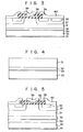
- Fig. 3 is a cross-sectional view showing a conductivity modulation type semiconductor device according to one embodiment of this invention;
- Fig. 4 is a cross-sectional view showing a silicon substrate assembly in the manufacturing process of the semiconductor device shown in Fig. 3; and
- Fig. 5 is a cross-sectional view showing a semiconductor device according to another embodiment of this invention.
- A conductivity modulation semiconductor device according to one embodiment of this invention will be explained below in connection with the manufacturing steps.
- The specific resistance and thickness of an N- type drain region are predetermined in order to obtain a desired source-to-drain withstand voltage. For example, the drain region has a specific resistance of 20 to 30 Ω·cm (an impurity concentration of below 1 x 1014cm-3) and thickness of 50 to 60 µm at a withstand voltage of 500 V and a specific resistance of 50 to 60 Ω·cm (an impurity concentration of below 1 x 10 14 cm-3) and thickness of about 100 µm at a withstand voltage of 1,000 V. To obtain such an impurity concentration, phosphorus, for example, may be used as a dopant.
- With these considerations, a planar N-
type silicon substrate 31 is prepared and an impurity, such as phosphorus, arsenic or antimony, is ion implanted into one surface portion of the silicon substrate and then the surface of the resultant structure is heat treated to form N+type silicon layer 32. Like the N-type silicon substrate, P+type silicon substrate 33 containing a boron of 1 x 10¹⁹ to 1021 cm-3, preferably 1 x 10²⁰, is prepared and it is joined to the N-type silicon substrate by the following method to provide an integral structure. - The N
type silicon substrate 31 and P+type silicon substrate 33 (anode substrate) are sheet-like in configuration and rigid in nature. First, the upper surface of the Ptype silicon substrate 33 and surface of the N-type silicon substrate 31 (N+type silicon layer 32) are mirror-polished to form first and second mirror faces having a surface roughness of below 500 A. Depending upon the surface conditions, a pretreatment process is carried out, using H202+H2S04-HF-diluted H, to eliminate a grease and stain film on the respective faces of the respective substrates. Then, the mirror faces of the silicon substrates are washed with clean water for a few minutes and dried by, for example, a spinner at room temperature. This process eliminates excessive moisture, while moisture assumed to have been absorbed on or in the silicon mirror faces of the respective substrates is left as it is. It is, therefore, necessary to avoid a heat-drying step at above 100°C at which such moisture evaporates. After such step, the silicon mirror faces are placed in a clean outer atmosphere of below Class 1 and intimately joined to each other with no foreign substance left therebetween, providing a semiconductor substrate assembly. In this connection it is to be noted that the outer atmosphere may be an inert atmosphere, such as nitrogen, or a reducing atmosphere. The semiconductor substrate assembly so obtained is heated at above 200°C, preferably 1,000 to 1,200°C to increase the joint strength between the silicon substrates. -
Junction 34 is formed by the joining step between the semiconductor substrates. The semiconductor assembly so obtained has no thermal nor electrical conduction barrier at the junction and a greater physical joint strength can be obtained at the junction. This structure can be treated in the same way as a single structure. - The resultant semiconductor assembly is of a P+-N+-N- structure. The surface of N-
type silicon substrate 31 is polished to a predetermined depth and, in this way, it is adjusted to a depth necessary for the aforementioned drain region. - At the next step, as in the case of a known VDMOSFET, a self-aligning method is used for the resultant structure with a polysilicon layer as a mask to provide a conductivity modulation type MOSFET.
- Approximately 1,000 A-thick
silicon dioxide layer 35 is deposited on the N-type silicon layer, i.e., on the exposed surface of the P+-N+-N- semiconductor structure and then a 2,000 to 3,000 A-thick polycrystalline layer forgate layer 36 as described below is selectively formed onsilicon dioxide layer 35. With the polysilicon layer as a mask, an N type impurity, such as boron, is ion implanted through the relatively thin silicon dioxide layer 35 (hereinafter referred to as an insulating layer) into N-type silicon substrate 31 and annealed to form a plurality of P type body regions 37. - Then, the insulating layer portion where the polysilicon layer is not deposited is removed by a photo- etching method to expose the surfaces of body regions 37. Arsenic or phosphorus is diffused into the exposed surface area of P type body region 37 to form two
N type regions 38, acting as source regions, in P type body region 37. Then, a CVD film is deposited onpolysilicon layer 36 to burypolysilicon layer 36 in the insulating layer, noting that the insulating layer is also covered on the exposed surface portion of the N-type silicon substrate, that is, on the surface portion ofN type region 38 and P type body region 37. - That portion of the insulating layer formed opposite to the polysilicon layer is removed and aluminum, for example, is deposited to provide
gate electrode 39. The aluminum is also deposited on P type body region 37 to providesource electrode 40. Furthermore, gold is deposited on the exposed surface of the P+type silicon substrate 33 to formanode electrode 41. In this way, a conductivity modulation type MOSFET can be produced. - The turn-off time was measured for a conventional semiconductor device and a semiconductor device manufactured according to this invention and found that it was 700 nsec for the conventional semiconductor device and 140 nsec for the present semiconductor device, noting that this measurement was carried out by a sample which uses a current density of 100A and an ON voltage of 2.5 V.
- A semiconductor device according to another embodiment of this invention is explained below with reference to Fig. 5.
- In the embodiment shown in Fig. 5, P-
type silicon layer 50 with a boron concentration of 1 x 10¹⁵ to 1018 cm-3 is deposited by the vapor growth method on a P+type silicon body thereby formingsilicon substrate 33. The resultant structure is joined at P-type silicon layer 50 tosilicon substrate 31. Then, the same manufacturing steps as those explained in connection with the first embodiment are carried out to provide a conductivity modulation type MOSFET. - In the first embodiment, since the impurity concentration of P+
type silicon substrate 33 is higher than that of N+type layer 32 ofsilicon substrate 31, impurity atoms contained in Ptype silicon substrate 33 are rediffused into N+type silicon layer 32 due to a heat load applied in the manufacturing process, causing an inversion layer to form on the N type silicon layer side due to a sequential inversion into a P type. The inversion layer is usually about 10 µm in thickness. In the first embodiment, for example, the N+type silicon layer initially forms at a thickness of 5 to 30 µm. In this way, the N+type silicon layer is formed such that the whole layer is prevented from being inverted due to a progressive rediffusion. - According to the second invention the aforementioned inversion phenomenon can be suppressed due to the presence of the P-type layer, so that control of a high impurity concentration layer is easier.
- As explained in more detail above, the conductivity modulation type semiconductor device of this invention can positively reduce the turn-off time to about one-fifth that of the conventional conductivity modulation type semiconductor device. The use of the present semiconductor device for motor control is thus to be expected.
- Furthermore, according to this invention the difficulty of mass-production is markedly decreased in comparison with the use of the vapor growth method, thus assuring lower costs due to mass-production.
as shown in Fig. 2.
Claims (7)
Priority Applications (1)
| Application Number | Priority Date | Filing Date | Title |
|---|---|---|---|
| EP90115990A EP0406916B1 (en) | 1985-02-20 | 1986-02-18 | Conductivity modulation type semiconductor device and method for manufacturing the same |
Applications Claiming Priority (2)
| Application Number | Priority Date | Filing Date | Title |
|---|---|---|---|
| JP30577/85 | 1985-02-20 | ||
| JP60030577A JPS61191071A (en) | 1985-02-20 | 1985-02-20 | Conductivity modulation type semiconductor device and manufacture thereof |
Related Child Applications (1)
| Application Number | Title | Priority Date | Filing Date |
|---|---|---|---|
| EP90115990.5 Division-Into | 1990-08-21 |
Publications (3)
| Publication Number | Publication Date |
|---|---|
| EP0192229A2 true EP0192229A2 (en) | 1986-08-27 |
| EP0192229A3 EP0192229A3 (en) | 1987-03-25 |
| EP0192229B1 EP0192229B1 (en) | 1991-07-24 |
Family
ID=12307706
Family Applications (2)
| Application Number | Title | Priority Date | Filing Date |
|---|---|---|---|
| EP86102047A Expired EP0192229B1 (en) | 1985-02-20 | 1986-02-18 | Conductivity modulation type semiconductor device and method for manufacturing the same |
| EP90115990A Expired - Lifetime EP0406916B1 (en) | 1985-02-20 | 1986-02-18 | Conductivity modulation type semiconductor device and method for manufacturing the same |
Family Applications After (1)
| Application Number | Title | Priority Date | Filing Date |
|---|---|---|---|
| EP90115990A Expired - Lifetime EP0406916B1 (en) | 1985-02-20 | 1986-02-18 | Conductivity modulation type semiconductor device and method for manufacturing the same |
Country Status (4)
| Country | Link |
|---|---|
| US (1) | US5128277A (en) |
| EP (2) | EP0192229B1 (en) |
| JP (1) | JPS61191071A (en) |
| DE (2) | DE3680352D1 (en) |
Cited By (10)
| Publication number | Priority date | Publication date | Assignee | Title |
|---|---|---|---|---|
| EP0269294A1 (en) * | 1986-11-05 | 1988-06-01 | Kabushiki Kaisha Toshiba | Method of manufacturing a bonded structure type semiconductor substrate |
| EP0365107A2 (en) * | 1988-10-19 | 1990-04-25 | Kabushiki Kaisha Toshiba | Manufacturing method for vertically conductive semiconductor devices |
| EP0405138A2 (en) * | 1989-05-26 | 1991-01-02 | Mitsubishi Denki Kabushiki Kaisha | Insulated gate bipolar transistor and method of making the same |
| WO1999046809A1 (en) * | 1998-03-09 | 1999-09-16 | Harris Corporation | Devices formable by low temperature direct bonding |
| US6274892B1 (en) | 1998-03-09 | 2001-08-14 | Intersil Americas Inc. | Devices formable by low temperature direct bonding |
| US8618582B2 (en) | 2011-09-11 | 2013-12-31 | Cree, Inc. | Edge termination structure employing recesses for edge termination elements |
| US8653534B2 (en) | 2008-05-21 | 2014-02-18 | Cree, Inc. | Junction Barrier Schottky diodes with current surge capability |
| US8664665B2 (en) | 2011-09-11 | 2014-03-04 | Cree, Inc. | Schottky diode employing recesses for elements of junction barrier array |
| US8680587B2 (en) | 2011-09-11 | 2014-03-25 | Cree, Inc. | Schottky diode |
| US9595618B2 (en) | 2010-03-08 | 2017-03-14 | Cree, Inc. | Semiconductor devices with heterojunction barrier regions and methods of fabricating same |
Families Citing this family (3)
| Publication number | Priority date | Publication date | Assignee | Title |
|---|---|---|---|---|
| JPH07107935B2 (en) * | 1988-02-04 | 1995-11-15 | 株式会社東芝 | Semiconductor device |
| JPH07263721A (en) * | 1994-03-25 | 1995-10-13 | Nippondenso Co Ltd | Semiconductor device and manufacture thereof |
| JP3906076B2 (en) * | 2001-01-31 | 2007-04-18 | 株式会社東芝 | Semiconductor device |
Citations (4)
| Publication number | Priority date | Publication date | Assignee | Title |
|---|---|---|---|---|
| DE1514727A1 (en) * | 1965-09-30 | 1969-06-19 | Schaefer Dipl Phys Siegfried | Production of pn junctions by plastic deformation of semiconductors |
| GB2072422A (en) * | 1980-03-25 | 1981-09-30 | Rca Corp | Power mosfet with an anode region |
| GB2088631A (en) * | 1980-12-02 | 1982-06-09 | Gen Electric | Field effect controlled semiconductor rectifier |
| EP0161740A2 (en) * | 1984-05-09 | 1985-11-21 | Kabushiki Kaisha Toshiba | Method of manufacturing semiconductor substrate |
Family Cites Families (12)
| Publication number | Priority date | Publication date | Assignee | Title |
|---|---|---|---|---|
| US3312880A (en) * | 1962-12-12 | 1967-04-04 | Sylvania Electric Prod | Four-layer semiconductor switching device having turn-on and turn-off gain |
| US3324359A (en) * | 1963-09-30 | 1967-06-06 | Gen Electric | Four layer semiconductor switch with the third layer defining a continuous, uninterrupted internal junction |
| US3659334A (en) * | 1970-10-13 | 1972-05-02 | Rca Corp | High power high frequency device |
| JPS4843590A (en) * | 1971-10-04 | 1973-06-23 | ||
| DE2926734C2 (en) * | 1979-07-03 | 1982-09-09 | Licentia Patent-Verwaltungs-Gmbh, 6000 Frankfurt | Thyristor with a pn junction produced by plastic deformation and a method for manufacturing it |
| US4383268A (en) * | 1980-07-07 | 1983-05-10 | Rca Corporation | High-current, high-voltage semiconductor devices having a metallurgical grade substrate |
| US4587713A (en) * | 1984-02-22 | 1986-05-13 | Rca Corporation | Method for making vertical MOSFET with reduced bipolar effects |
| US4631564A (en) * | 1984-10-23 | 1986-12-23 | Rca Corporation | Gate shield structure for power MOS device |
| JPH0770474B2 (en) * | 1985-02-08 | 1995-07-31 | 株式会社東芝 | Method for manufacturing compound semiconductor device |
| US4639754A (en) * | 1985-02-25 | 1987-01-27 | Rca Corporation | Vertical MOSFET with diminished bipolar effects |
| JPS6350013A (en) * | 1986-08-20 | 1988-03-02 | Meidensha Electric Mfg Co Ltd | Manufacture of semiconductor device |
| JP2579979B2 (en) * | 1987-02-26 | 1997-02-12 | 株式会社東芝 | Method for manufacturing semiconductor device |
-
1985
- 1985-02-20 JP JP60030577A patent/JPS61191071A/en active Granted
-
1986
- 1986-02-18 DE DE8686102047T patent/DE3680352D1/en not_active Expired - Lifetime
- 1986-02-18 EP EP86102047A patent/EP0192229B1/en not_active Expired
- 1986-02-18 EP EP90115990A patent/EP0406916B1/en not_active Expired - Lifetime
- 1986-02-18 DE DE3650573T patent/DE3650573T2/en not_active Expired - Lifetime
-
1990
- 1990-10-03 US US07/593,461 patent/US5128277A/en not_active Expired - Lifetime
Patent Citations (4)
| Publication number | Priority date | Publication date | Assignee | Title |
|---|---|---|---|---|
| DE1514727A1 (en) * | 1965-09-30 | 1969-06-19 | Schaefer Dipl Phys Siegfried | Production of pn junctions by plastic deformation of semiconductors |
| GB2072422A (en) * | 1980-03-25 | 1981-09-30 | Rca Corp | Power mosfet with an anode region |
| GB2088631A (en) * | 1980-12-02 | 1982-06-09 | Gen Electric | Field effect controlled semiconductor rectifier |
| EP0161740A2 (en) * | 1984-05-09 | 1985-11-21 | Kabushiki Kaisha Toshiba | Method of manufacturing semiconductor substrate |
Non-Patent Citations (1)
| Title |
|---|
| INTERNATIONAL ELECTRON DEVICES MEETING, TECHNICAL DIGEST, Washington, D.C., 5th-7th December 1983, pages 79-82, IEEE, New York, US; A.M. GOODMAN et al.: "Improved COMFETs with fast switching speed and high-current capability" * |
Cited By (17)
| Publication number | Priority date | Publication date | Assignee | Title |
|---|---|---|---|---|
| EP0269294A1 (en) * | 1986-11-05 | 1988-06-01 | Kabushiki Kaisha Toshiba | Method of manufacturing a bonded structure type semiconductor substrate |
| EP0365107A2 (en) * | 1988-10-19 | 1990-04-25 | Kabushiki Kaisha Toshiba | Manufacturing method for vertically conductive semiconductor devices |
| EP0365107A3 (en) * | 1988-10-19 | 1991-01-02 | Kabushiki Kaisha Toshiba | Manufacturing method for vertically conductive semiconductor devices |
| EP0405138A2 (en) * | 1989-05-26 | 1991-01-02 | Mitsubishi Denki Kabushiki Kaisha | Insulated gate bipolar transistor and method of making the same |
| EP0405138A3 (en) * | 1989-05-26 | 1991-11-27 | Mitsubishi Denki Kabushiki Kaisha | Insulated gate bipolar transistors and methods of making the same |
| US5170239A (en) * | 1989-05-26 | 1992-12-08 | Mitsubishi Denki Kabushiki Kaisha | Insulated gate bipolar transistor having high short-circuit SOA and high latch-up current |
| US5391898A (en) * | 1989-05-26 | 1995-02-21 | Mitsubishi Denki Kabushiki Kaisha | Insulated gate bipolar transistor having high short-circuit and latch-up withstandability |
| EP0690512A1 (en) * | 1989-05-26 | 1996-01-03 | Mitsubishi Denki Kabushiki Kaisha | Insulated gate bipolar transistor and method for fabricating the same |
| WO1999046809A1 (en) * | 1998-03-09 | 1999-09-16 | Harris Corporation | Devices formable by low temperature direct bonding |
| US6274892B1 (en) | 1998-03-09 | 2001-08-14 | Intersil Americas Inc. | Devices formable by low temperature direct bonding |
| US8653534B2 (en) | 2008-05-21 | 2014-02-18 | Cree, Inc. | Junction Barrier Schottky diodes with current surge capability |
| US9595618B2 (en) | 2010-03-08 | 2017-03-14 | Cree, Inc. | Semiconductor devices with heterojunction barrier regions and methods of fabricating same |
| US8618582B2 (en) | 2011-09-11 | 2013-12-31 | Cree, Inc. | Edge termination structure employing recesses for edge termination elements |
| US8664665B2 (en) | 2011-09-11 | 2014-03-04 | Cree, Inc. | Schottky diode employing recesses for elements of junction barrier array |
| US8680587B2 (en) | 2011-09-11 | 2014-03-25 | Cree, Inc. | Schottky diode |
| US9231122B2 (en) | 2011-09-11 | 2016-01-05 | Cree, Inc. | Schottky diode |
| US9865750B2 (en) | 2011-09-11 | 2018-01-09 | Cree, Inc. | Schottky diode |
Also Published As
| Publication number | Publication date |
|---|---|
| JPH0544835B2 (en) | 1993-07-07 |
| EP0406916B1 (en) | 1996-09-25 |
| EP0406916A3 (en) | 1991-08-28 |
| US5128277A (en) | 1992-07-07 |
| DE3650573T2 (en) | 1997-03-06 |
| DE3680352D1 (en) | 1991-08-29 |
| JPS61191071A (en) | 1986-08-25 |
| EP0192229A3 (en) | 1987-03-25 |
| EP0192229B1 (en) | 1991-07-24 |
| DE3650573D1 (en) | 1996-10-31 |
| EP0406916A2 (en) | 1991-01-09 |
Similar Documents
| Publication | Publication Date | Title |
|---|---|---|
| KR100596061B1 (en) | Self-aligned methods of fabricating silicon carbide power devices by implantation and lateral diffusions | |
| US4935386A (en) | Method of manufacturing semiconductor device including substrate bonding and outdiffusion by thermal heating | |
| EP0181091B1 (en) | Schottky gate field effect transistor and manufacturing method thereof | |
| US5933733A (en) | Zero thermal budget manufacturing process for MOS-technology power devices | |
| EP0488440B1 (en) | Process of introduction and diffusion of platinum ions in a slice of silicon | |
| EP0190935A2 (en) | Method of manufacturing semiconductor devices using a bonding process | |
| EP0192229B1 (en) | Conductivity modulation type semiconductor device and method for manufacturing the same | |
| KR100391560B1 (en) | A semiconductor device | |
| JPH09232567A (en) | Mos gate power device and manufacture thereof | |
| US4662058A (en) | Self-aligned gate process for ICS based on modulation doped (Al,Ga) As/GaAs FETs | |
| CA1112374A (en) | Method for forming self-aligned field effect device by ion implantation | |
| US5874338A (en) | MOS-technology power device and process of making same | |
| US4498224A (en) | Method of manufacturing a MOSFET using accelerated ions to form an amorphous region | |
| JPH0578949B2 (en) | ||
| US5753943A (en) | Insulated gate type field effect transistor and method of manufacturing the same | |
| US3860454A (en) | Field effect transistor structure for minimizing parasitic inversion and process for fabricating | |
| US3946419A (en) | Field effect transistor structure for minimizing parasitic inversion and process for fabricating | |
| US4216038A (en) | Semiconductor device and manufacturing process thereof | |
| GB2074374A (en) | Method of making field effect transistors | |
| JPH04206933A (en) | Semiconductor device | |
| JP2688678B2 (en) | Field effect transistor and method of manufacturing the same | |
| Campbell et al. | Trapezoidal-groove Schottky-gate vertical-channel GaAs FET (GaAs static induction transistor) | |
| JPS6027173A (en) | Field effect transistor and manufacture thereof | |
| JPH02159070A (en) | Semiconductor device and manufacture thereof | |
| JPS62163372A (en) | Field effect semiconductor device |
Legal Events
| Date | Code | Title | Description |
|---|---|---|---|
| PUAI | Public reference made under article 153(3) epc to a published international application that has entered the european phase |
Free format text: ORIGINAL CODE: 0009012 |
|
| 17P | Request for examination filed |
Effective date: 19860218 |
|
| AK | Designated contracting states |
Kind code of ref document: A2 Designated state(s): DE FR GB |
|
| PUAL | Search report despatched |
Free format text: ORIGINAL CODE: 0009013 |
|
| AK | Designated contracting states |
Kind code of ref document: A3 Designated state(s): DE FR GB |
|
| 17Q | First examination report despatched |
Effective date: 19890323 |
|
| GRAA | (expected) grant |
Free format text: ORIGINAL CODE: 0009210 |
|
| AK | Designated contracting states |
Kind code of ref document: B1 Designated state(s): DE FR GB |
|
| XX | Miscellaneous (additional remarks) |
Free format text: TEILANMELDUNG 90115990.5 EINGEREICHT AM 18/02/86. |
|
| REF | Corresponds to: |
Ref document number: 3680352 Country of ref document: DE Date of ref document: 19910829 |
|
| ET | Fr: translation filed | ||
| PLBE | No opposition filed within time limit |
Free format text: ORIGINAL CODE: 0009261 |
|
| STAA | Information on the status of an ep patent application or granted ep patent |
Free format text: STATUS: NO OPPOSITION FILED WITHIN TIME LIMIT |
|
| 26N | No opposition filed | ||
| REG | Reference to a national code |
Ref country code: GB Ref legal event code: 746 Effective date: 19981007 |
|
| REG | Reference to a national code |
Ref country code: FR Ref legal event code: D6 |
|
| REG | Reference to a national code |
Ref country code: GB Ref legal event code: IF02 |
|
| PGFP | Annual fee paid to national office [announced via postgrant information from national office to epo] |
Ref country code: FR Payment date: 20050208 Year of fee payment: 20 |
|
| PGFP | Annual fee paid to national office [announced via postgrant information from national office to epo] |
Ref country code: DE Payment date: 20050210 Year of fee payment: 20 |
|
| PGFP | Annual fee paid to national office [announced via postgrant information from national office to epo] |
Ref country code: GB Payment date: 20050216 Year of fee payment: 20 |
|
| REG | Reference to a national code |
Ref country code: GB Ref legal event code: PE20 |
|
| PG25 | Lapsed in a contracting state [announced via postgrant information from national office to epo] |
Ref country code: GB Free format text: LAPSE BECAUSE OF EXPIRATION OF PROTECTION Effective date: 20060217 |