EP0187504A2 - Digital phase correlator - Google Patents
Digital phase correlator Download PDFInfo
- Publication number
- EP0187504A2 EP0187504A2 EP85309222A EP85309222A EP0187504A2 EP 0187504 A2 EP0187504 A2 EP 0187504A2 EP 85309222 A EP85309222 A EP 85309222A EP 85309222 A EP85309222 A EP 85309222A EP 0187504 A2 EP0187504 A2 EP 0187504A2
- Authority
- EP
- European Patent Office
- Prior art keywords
- phase
- clock
- signal
- signals
- delay
- Prior art date
- Legal status (The legal status is an assumption and is not a legal conclusion. Google has not performed a legal analysis and makes no representation as to the accuracy of the status listed.)
- Withdrawn
Links
- 230000003111 delayed effect Effects 0.000 claims description 12
- 238000001514 detection method Methods 0.000 claims description 4
- 230000001934 delay Effects 0.000 claims description 3
- 238000004891 communication Methods 0.000 description 8
- 238000000034 method Methods 0.000 description 3
- 240000007320 Pinus strobus Species 0.000 description 2
- 238000005516 engineering process Methods 0.000 description 2
- 230000001360 synchronised effect Effects 0.000 description 2
- 230000005540 biological transmission Effects 0.000 description 1
- 238000012937 correction Methods 0.000 description 1
- 230000003247 decreasing effect Effects 0.000 description 1
- 238000010586 diagram Methods 0.000 description 1
- 238000004519 manufacturing process Methods 0.000 description 1
- 239000002184 metal Substances 0.000 description 1
- 238000012986 modification Methods 0.000 description 1
- 230000004048 modification Effects 0.000 description 1
- 238000010587 phase diagram Methods 0.000 description 1
- 230000000717 retained effect Effects 0.000 description 1
Images

Classifications
-
- H—ELECTRICITY
- H04—ELECTRIC COMMUNICATION TECHNIQUE
- H04L—TRANSMISSION OF DIGITAL INFORMATION, e.g. TELEGRAPHIC COMMUNICATION
- H04L7/00—Arrangements for synchronising receiver with transmitter
- H04L7/0008—Synchronisation information channels, e.g. clock distribution lines
- H04L7/0012—Synchronisation information channels, e.g. clock distribution lines by comparing receiver clock with transmitter clock
-
- H—ELECTRICITY
- H04—ELECTRIC COMMUNICATION TECHNIQUE
- H04L—TRANSMISSION OF DIGITAL INFORMATION, e.g. TELEGRAPHIC COMMUNICATION
- H04L7/00—Arrangements for synchronising receiver with transmitter
- H04L7/0016—Arrangements for synchronising receiver with transmitter correction of synchronization errors
- H04L7/0033—Correction by delay
- H04L7/0037—Delay of clock signal
Definitions
- the present invention relates generally to phase correlation, and more particularly to a digital phase correlator having particular utility in synchronizing high-frequency signals.
- Timing or clock signals are used to control practically all digital operations to ensure that the logical operations carried out in a digital system are performed at the correct times and in the proper sequence.
- Digital systems which employ clock signals include digital data-communication systems and computers and microprocessors. Many digital communication systems operate in response to a received or incoming clock signal and a free-running, internally generated clock system. For proper operation these clock signals must be properly synchronized; that is, the phase differences between them must be maintained at a minimum.
- Analog phase-locked loops which have long been used in computer and digital communication systems to synchronize clocks of different frequencies and phases, are feedback systems that include a phase comparator, a low-pass filter and an error amplifier in the forward signal path, and a voltage-controlled oscillator in the feedback path.
- the error voltage is equal to zero.
- the voltage-controlled oscillator operates at a set frequency. If an input signal is applied to the system, the phase comparator compares the phase and the frequency of the input with the voltage-controlled oscillator frequency and generates an error voltage that is related to the phase and frequency differences between the two signals. This error voltage is then filtered, amplified and applied to the control terminal of the voltage-controlled oscillator.
- the control voltage forces the frequency and phase of the voltage-controlled oscillator to vary in a direction that reduces the frequency and phase differences between the output of the voltage-controlled oscillator and the input signal.
- phase-locked loop The total time taken by the phase-locked loop to establish phase lock depends on the initial frequency and phase differences between the two clock signals, as well as on the overall loop gain and the low-pass filter bandwidth. This pull- in time is relatively slow and cannot match the speed of fast digital communication systems, which require very high-speed clock phase correlation. For this reason the analog phase-locked loop systems now commercially available can operate only at frequencies of up to 35 mHz.
- Digital phase-locked loop systems are also known and have been used, particularly in higher-speed applications. These digital phase-locked systems employ an EXCLUSIVE-OR gate to generate the phase error between the input and output signals and an up-down counter to replace the voltage-controlled oscillator in the analog phase-locked loop.
- the accuracy of the digital phase-locked loop depends on the accuracy of the fundamental clock and the loop propagation delays.
- the fundamental clock In order to maintain an acceptable accuracy in a digital phase-locked loop, the fundamental clock must have a frequency 16 or more times higher than that of the input and output signals. When the input and output signal frequencies reach the speed limit of digital components used in typical high-speed computer and digital communication systems, the much higher frequency requirement of the fundamental clock can no longer be met by any available digital components. The current, commercially available digital phase-locked loop can thus operate only up to 50 mHz.
- the control circuits namely the phase detector and phase- correction circuit, both operate at lower frequencies than the locked clock signals.
- the digital phase correlator comprises a delay line, a multiplexer, a rotating register and two phase detection flip-flops.
- two clocks with the same frequency land different phase come into the digital correlator, one of the clocks is delayed by the delay line. This delayed clock and the other clock are fed into the phase detection flip-flops to detect the phase difference between the two clocks.
- the initial delay on one clock is either increased or decreased by rotating the single ONE bit in the rotating register to the right or left, thereby to delay one of the clocks by a correct amount and thereby bring the two clocks toward phase synchronization with one another.
- the present invention relates to a high-speed digital phase correlator, substantially as defined in the appended claims and as described in the accompanying specification as considered in connection with the accompanying drawings in which:
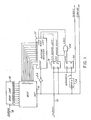
- Fig. 1 there is shown in schematic form an embodiment of the digital phase correlator of the present invention, which receives two clock signals Clock 1 and Clock 2 at lines 10 and 12, respectively.
- Clock 2 is applied to an input of a multitap delay line 14, having a plurality, here, for illustrative purposes, 10'taps, which provides delays at equal increments of ⁇ .
- the delay provided to Clock 2 at tap 4 ⁇ is four times the incremental delay ⁇ .
- the undelayed Clock 2 as well as the outputs of the taps of delay line 14 are applied as the inputs of a switching means or multiplexer 16.
- the other input clock Clock 1 is applied to the data or D inputs of phase-detect flip-flops 18 and 20.
- the two outputs of flip-flop 18, F F 1 and its inverse FF1 are applied respectively to the rotate left and rotate right control inputs of a rotating shift register 22, the plural stages of which are connected to the select lines of multiplexer 16.
- the output of multiplexer 16 which is the delayed Clock 2 signal or Clock 2D, is applied to the input of an nverter 24, the output of which is applied to the clock input of rotating register 22.
- the Clock 2D signal is also applied to the clock or C input of flip-flop 18 and to a fixed delay line 26 which introduces an additional delay of ⁇ .
- the output of delay line 26, which is Clock 2D + ⁇ , is applied to the clock or C input of flip-flop 20.
- the output FF2 of flip-flop 20 is applied, along with the output FF1 of flip-flop 18; to the inputs of an AND gate 28 the output of which is applied to the lock control input of register 22.
- a logic ONE signal is present in only one of the plurality of stages or bits 0, ⁇ , 2 ⁇ , 3 ⁇
- the ONE bit can be shifted between adjacent stages of rotating register 22 either to the right or to the left in response to a right or left shift control signal applied to the corresponding control input of the register.
- the ONE bit is retained or locked in its bit location when a signal is applied to the lock control input of the register.
- a corresponding tap or output of the delay line 14 is enabled, that is, switched to the output of the multiplexer 16 as the delayed Clock 2D signal. That is, for example, if the ONE is located in the 8 ⁇ bit of rotating register 22, the 8 ⁇ tap of delay line 14 is connected through the multiplexer 16 to the phase-detect flip-flops 18 and 20, such that the Clock 2 input on input line 12 is delayed by 8 ⁇ . Similarly, if the ONE is located in the 4 ⁇ bit of register 22, the 4 ⁇ tap of delay line 14 is selected by multiplexer 16 and the Clock 2D signal is, in this case, the Clock 2 signal delayed by 4 ⁇ .
- phase differences between the Clock 1 and Clock 2D are detected by the phase-detect flip-flops 18 and 20 in the manner now described.
- Fig. 2 illustrates the four conditions of relative phase between the Clock 1, Clock 2D and Clock 2D + D signals.
- Clock 1 leads Clock 2D but the leading edges of Clock 2D and Clock 2D + D both lead the falling or trailing edge of Clock 1.
- Clock 1 again leads Clock 2 D but the leading edge of Clock 2D + ⁇ occurs later than the trailing edge of Clock 1.
- Clock 2 D and Clock 2D + ⁇ both lead Clock 1
- Fig. 2d Clock 1 and Clock 2D + ⁇ are in phase.
- the Clock 2D signal strobes a ONE into flip-flop 18 and the delayed Clock 2D + ⁇ signal strobes a ONE into flip-flop 20 in the first condition (Fig. 2a), and a ZERO into flip-flop 20 in the second condition (Fig. 2b).
- FF1 ONE
- FF 2 redundant and need not be used in this decision
- Clock 1 is always leading Clock 2D and Clock 2D must be shifted to the left to reduce the phase difference between these clock signals.
- a rotate left signal is sent to the'rotating register 22 to cause the ONE bit to be shifted one position to the left.
- the rotating register 22 is preferably initialized by establishing the ONE bit at the 5 ⁇ position; after the first left shift, it moves to the 4 position).
- This 4 ⁇ position selects a 4 A delay from the delay line 14 through the multiplexer 16, as described above, thus moving Clock 2D one ⁇ position to the left. This process reduces by one ⁇ the phase difference between Clock 1 and Clock 2D.
- AND gate 28 combines the FF1 output of flip-flop 18 and the FF2 output of flip-flop 20 into .a lock signal to lock the ONE bit in its current bit location in rotating register 22, thereby to lock Clock 1 and Clock 2D in phase.
- the delay line 14 can be of the R-C type, or may be precision metal lines as in a VLSI circuit. Since in VLSI fabrication such a delay line;can be very accurate and each increment A can be in the picosecond (10 -12 second) range, very high-speed and accurate digital phase correlatior can be implemented with VLSI technology.
- the digital phase correlator of the present invention provides significant advantages over the conventional digital phase-locked loop in that the digital correlator of the invention makes use of the input clock to detect and adjust the phase difference of two input clocks.
- the operating speed of the digital phase correlator of the invention is thus the same as that of the input clocks, as compared to conventional digital phase-locked loops, which use a master clock at a frequency 16 or more times greater than that of the input clocks to detect and adjust phase differences.
- the digital phase correlator of the present invention can thus expand the speed limit of phase correlation by a factor of 16 or more as compared to the conventional digital phase-locked loops.
Abstract
Description
- The present invention relates generally to phase correlation, and more particularly to a digital phase correlator having particular utility in synchronizing high-frequency signals.
- Timing or clock signals are used to control practically all digital operations to ensure that the logical operations carried out in a digital system are performed at the correct times and in the proper sequence. Digital systems which employ clock signals include digital data-communication systems and computers and microprocessors. Many digital communication systems operate in response to a received or incoming clock signal and a free-running, internally generated clock system. For proper operation these clock signals must be properly synchronized; that is, the phase differences between them must be maintained at a minimum.
- In recent years the demand for data transmissions at ever-increasing rates has resulted in the requirement for clock signals at ever-increasing frequencies, such that clock frequencies in the order of 60-100 mHz and higher are commonly utilized.
- Analog phase-locked loops, which have long been used in computer and digital communication systems to synchronize clocks of different frequencies and phases, are feedback systems that include a phase comparator, a low-pass filter and an error amplifier in the forward signal path, and a voltage-controlled oscillator in the feedback path. When no input signal is applied to the system, the error voltage is equal to zero. The voltage-controlled oscillator operates at a set frequency. If an input signal is applied to the system, the phase comparator compares the phase and the frequency of the input with the voltage-controlled oscillator frequency and generates an error voltage that is related to the phase and frequency differences between the two signals. This error voltage is then filtered, amplified and applied to the control terminal of the voltage-controlled oscillator. The control voltage forces the frequency and phase of the voltage-controlled oscillator to vary in a direction that reduces the frequency and phase differences between the output of the voltage-controlled oscillator and the input signal.
- The total time taken by the phase-locked loop to establish phase lock depends on the initial frequency and phase differences between the two clock signals, as well as on the overall loop gain and the low-pass filter bandwidth. This pull- in time is relatively slow and cannot match the speed of fast digital communication systems, which require very high-speed clock phase correlation. For this reason the analog phase-locked loop systems now commercially available can operate only at frequencies of up to 35 mHz.
- Digital phase-locked loop systems are also known and have been used, particularly in higher-speed applications. These digital phase-locked systems employ an EXCLUSIVE-OR gate to generate the phase error between the input and output signals and an up-down counter to replace the voltage-controlled oscillator in the analog phase-locked loop. The accuracy of the digital phase-locked loop depends on the accuracy of the fundamental clock and the loop propagation delays.
- In order to maintain an acceptable accuracy in a digital phase-locked loop, the fundamental clock must have a frequency 16 or more times higher than that of the input and output signals. When the input and output signal frequencies reach the speed limit of digital components used in typical high-speed computer and digital communication systems, the much higher frequency requirement of the fundamental clock can no longer be met by any available digital components. The current, commercially available digital phase-locked loop can thus operate only up to 50 mHz.
- For high-speed computer and digital communication systems with data rates of 100 mHz or more, complicated custom circuits are required to synchronize the phases of two different clocks. These circuits are very expensive to fabricate and very difficult to maintain. As a result of the rapid advancement in digital communication technologies, there is a need for a high-speed digital phase correlator that can be fabricated with commercially available and relatively low-cost digital components.
- In an effort to satisfy this need, designs have been proposed.to provide synchronization of high-frequency clock pulses by digital means other than in a phase-locked loop, such as those shown in U.S. Patent Nos. 4,012,598 and 4,386,323. However, none of these devices are capable of operating at high frequencies in the range of 50 mHz or greater such that there is still a need for a practical low-cost, high-speed digital phase .correlator.
- It is an object of the present invention to provide a digital phase correlator capable of providing synchronization for high-frequency clock signals.
- It is a further object of the present invention to provide a digital phase correlator of the type described which makes use of conventional digital components and is thus relatively low in cost and has a relatively low power consumption.
- It is another, more general object of the present invention to provide a low-cost, high-speed digital phase correlator.
- In the digital phase correlator of the present invention, the control circuits, namely the phase detector and phase- correction circuit, both operate at lower frequencies than the locked clock signals. The digital phase correlator comprises a delay line, a multiplexer, a rotating register and two phase detection flip-flops. When two clocks with the same frequency land different phase come into the digital correlator, one of the clocks is delayed by the delay line. This delayed clock and the other clock are fed into the phase detection flip-flops to detect the phase difference between the two clocks. Depending on the result of this phase detection, the initial delay on one clock is either increased or decreased by rotating the single ONE bit in the rotating register to the right or left, thereby to delay one of the clocks by a correct amount and thereby bring the two clocks toward phase synchronization with one another.
- To the accomplishment of the above and such further objects as may hereinafter appear, the present invention relates to a high-speed digital phase correlator, substantially as defined in the appended claims and as described in the accompanying specification as considered in connection with the accompanying drawings in which:
- Fig. 1 is a schematic diagram of an embodiment of a digital phase correlator in accordance with the present invention; and
- Figs. 2a - 2d illustrate the various phase relations of the two clocks and the resulting conditions of the phase-detect flip-flops in the digital phase correlator of Fig. 1.
- Referring to Fig. 1, there is shown in schematic form an embodiment of the digital phase correlator of the present invention, which receives two
clock signals Clock 1 andClock 2 atlines Clock 2 is applied to an input of amultitap delay line 14, having a plurality, here, for illustrative purposes, 10'taps, which provides delays at equal increments of Δ. Thus, the delay provided toClock 2 at tap 4 Δ is four times the incremental delay Δ. Theundelayed Clock 2 as well as the outputs of the taps ofdelay line 14 are applied as the inputs of a switching means or multiplexer 16. - The other
input clock Clock 1 is applied to the data or D inputs of phase-detect flip-flops flop 18,F F1 and its inverse FF1, are applied respectively to the rotate left and rotate right control inputs of arotating shift register 22, the plural stages of which are connected to the select lines of multiplexer 16. - The output of multiplexer 16, which is the
delayed Clock 2 signal orClock 2D, is applied to the input of annverter 24, the output of which is applied to the clock input of rotatingregister 22. TheClock 2D signal is also applied to the clock or C input of flip-flop 18 and to a fixed delay line 26 which introduces an additional delay of Δ. The output of delay line 26, which isClock 2D + Δ, is applied to the clock or C input of flip-flop 20. The output FF2 of flip-flop 20 is applied, along with the output FF1 of flip-flop 18; to the inputs of anAND gate 28 the output of which is applied to the lock control input ofregister 22. - As a result of the operation of the digital phase correlator of Fig. 1, which is now described with reference to the flip-flop condition and phase diagrams of Fig. 2,
Clock 1 andClock 2D are maintained in accurate phase synchronization. - In the operation of the
rotating register 22, as is known to those skilled in the art, a logic ONE signal is present in only one of the plurality of stages orbits 0, Δ, 2 Δ, 3 Δ - ...10Δ. Moreover, the ONE bit can be shifted between adjacent stages of rotating
register 22 either to the right or to the left in response to a right or left shift control signal applied to the corresponding control input of the register. Alternatively, the ONE bit is retained or locked in its bit location when a signal is applied to the lock control input of the register. - Depending on which bit of the rotating shift register contains the logic ONE, a corresponding tap or output of the
delay line 14 is enabled, that is, switched to the output of the multiplexer 16 as thedelayed Clock 2D signal. That is, for example, if the ONE is located in the 8 Δ bit of rotatingregister 22, the 8 Δ tap ofdelay line 14 is connected through the multiplexer 16 to the phase-detect flip-flops Clock 2 input oninput line 12 is delayed by 8 Δ. Similarly, if the ONE is located in the 4 Δ bit ofregister 22, the 4 Δ tap ofdelay line 14 is selected by multiplexer 16 and theClock 2D signal is, in this case, theClock 2 signal delayed by 4 Δ. - The phase differences between the
Clock 1 andClock 2D are detected by the phase-detect flip-flops - Fig. 2 illustrates the four conditions of relative phase between the
Clock 1,Clock 2D andClock 2D + D signals. In the first condition (Fig. 2a),Clock 1 leadsClock 2D but the leading edges ofClock 2D andClock 2D + D both lead the falling or trailing edge ofClock 1. In the second condition (Fig. 2b),Clock 1 again leadsClock 2D but the leading edge ofClock 2D + Δ occurs later than the trailing edge ofClock 1. In the third condition (Fig. 2c),Clock 2D andClock 2D + Δ both leadClock 1, and in the fourth condition (Fig. 2d),Clock 1 andClock 2D + Δ are in phase. - As shown in Figs. 2a and 2b, the
Clock 2D signal strobes a ONE into flip-flop 18 and the delayedClock 2D + Δ signal strobes a ONE into flip-flop 20 in the first condition (Fig. 2a), and a ZERO into flip-flop 20 in the second condition (Fig. 2b). This implies that when FF1 is ONE (FF2 is redundant and need not be used in this decision),Clock 1 is always leadingClock 2D andClock 2D must be shifted to the left to reduce the phase difference between these clock signals. When FF1 is ONE, a rotate left signal is sent to the'rotating register 22 to cause the ONE bit to be shifted one position to the left. (Therotating register 22 is preferably initialized by establishing the ONE bit at the 5 Δ position; after the first left shift, it moves to the 4 position). This 4 Δ position, in turn, selects a 4 A delay from thedelay line 14 through the multiplexer 16, as described above, thus movingClock 2D one Δ position to the left. This process reduces by one Δ the phase difference betweenClock 1 andClock 2D. - In the next clock cycle, if
Clock 1 is still leadingClock 2D, the FF1 output of flip-flop 18 is set to ONE again at the leading edge ofClock 2D, and rotating register.22 is again shifted one position to the left on the trailing edge ofClock 2D to shift the ONE bit to the 3 A position. This removes another Δ away from thedelay line 14 and movesClock 2D one increment further closer toClock 1. This process continues untilClock 1 and Clock. 2D are in phase (Fig. 2d). The in-phase condition is detected when the FF1 output of flip-flop 18 is ZERO and the FF2 output of flip-flop 20 is set to ONE as shown in Fig. 2d. When this condition occurs, ANDgate 28 combines the FF1 output of flip-flop 18 and the FF2 output of flip-flop 20 into .a lock signal to lock the ONE bit in its current bit location in rotatingregister 22, thereby to lockClock 1 andClock 2D in phase. - It should be noted that although the input ;
clocks Clock 1 andClock 2 are out of phase, theoutput clocks Clock 1 andClock 2D are in phase after a few clock cycles and can be used as synchronized clocks for computer and data-communication systems. - When
Clock 2D is leadingClock 1, (Fig. 2c) the FF1 and FF2 outputs of flip-flops rotating register 22 is rotated one position to the right (initially from the 5 A to the 6 Δ position.) This adds one Δ to the delay ofClock 2D and movesClock 2D one A position to the right. IfClock 2D is still leadingClock 1 after the first cycle, the process is repeated untilClock 1 andClock 2D are in phase and then locked in phase as described above. Thedelay line 14 can be of the R-C type, or may be precision metal lines as in a VLSI circuit. Since in VLSI fabrication such a delay line;can be very accurate and each increment A can be in the picosecond (10-12 second) range, very high-speed and accurate digital phase correlatior can be implemented with VLSI technology. - It will thus be appreciated that the digital phase correlator of the present invention provides significant advantages over the conventional digital phase-locked loop in that the digital correlator of the invention makes use of the input clock to detect and adjust the phase difference of two input clocks. The operating speed of the digital phase correlator of the invention is thus the same as that of the input clocks, as compared to conventional digital phase-locked loops, which use a master clock at a frequency 16 or more times greater than that of the input clocks to detect and adjust phase differences. The digital phase correlator of the present invention can thus expand the speed limit of phase correlation by a factor of 16 or more as compared to the conventional digital phase-locked loops.
- It will also be appreciated that other modifications may be made to the embodiment of the digital phase correlator described hereinabove, other than those specifically suggested, without necessarily departing from the spirit and scope of the invention.
Claims (6)
Applications Claiming Priority (2)
| Application Number | Priority Date | Filing Date | Title |
|---|---|---|---|
| US06/689,072 US4604582A (en) | 1985-01-04 | 1985-01-04 | Digital phase correlator |
| US689072 | 1985-01-04 |
Publications (2)
| Publication Number | Publication Date |
|---|---|
| EP0187504A2 true EP0187504A2 (en) | 1986-07-16 |
| EP0187504A3 EP0187504A3 (en) | 1986-10-08 |
Family
ID=24766934
Family Applications (1)
| Application Number | Title | Priority Date | Filing Date |
|---|---|---|---|
| EP85309222A Withdrawn EP0187504A3 (en) | 1985-01-04 | 1985-12-18 | Digital phase correlator |
Country Status (4)
| Country | Link |
|---|---|
| US (1) | US4604582A (en) |
| EP (1) | EP0187504A3 (en) |
| JP (1) | JPS61163745A (en) |
| CA (1) | CA1215750A (en) |
Cited By (4)
| Publication number | Priority date | Publication date | Assignee | Title |
|---|---|---|---|---|
| FR2608871A1 (en) * | 1986-12-18 | 1988-06-24 | Cit Alcatel | Time-division method of multiplexing and demultiplexing synchronous digital streams |
| EP0317821A2 (en) * | 1987-11-25 | 1989-05-31 | Siemens Aktiengesellschaft | High resolution digital phase-lock loop circuit |
| EP0369047A1 (en) * | 1988-11-15 | 1990-05-23 | Siemens Aktiengesellschaft | Arrangement for commuting a clock on a clock with the same frequency but lagging in phase |
| EP0531166A1 (en) * | 1991-09-06 | 1993-03-10 | Xerox Corporation | Seam-less data recovery |
Families Citing this family (44)
| Publication number | Priority date | Publication date | Assignee | Title |
|---|---|---|---|---|
| US4845437A (en) * | 1985-07-09 | 1989-07-04 | Minolta Camera Kabushiki Kaisha | Synchronous clock frequency conversion circuit |
| JPS62276935A (en) * | 1986-01-07 | 1987-12-01 | Fujitsu Ltd | Multiplexer |
| US4756011A (en) * | 1986-12-24 | 1988-07-05 | Bell Communications Research, Inc. | Digital phase aligner |
| US4857868A (en) * | 1988-03-30 | 1989-08-15 | Rockwell International Corporation | Data driven clock generator |
| US4965815A (en) * | 1988-07-21 | 1990-10-23 | U.S. Philips Corporation | Phase detection circuit for stepwise measurement of a phase relation |
| US4998262A (en) * | 1989-10-10 | 1991-03-05 | Hewlett-Packard Company | Generation of topology independent reference signals |
| CA2001266C (en) * | 1989-10-23 | 1996-08-06 | John Robert Long | Digital phase aligner and method for its operation |
| US5079440A (en) * | 1990-03-15 | 1992-01-07 | Intel Corporation | Apparatus for generating computer clock pulses |
| US5045715A (en) * | 1990-03-19 | 1991-09-03 | Apple Computer, Inc. | Circuit for generating stretched clock phases on a cycle by cycle basis |
| US4985640A (en) * | 1990-04-04 | 1991-01-15 | Intel Corporation | Apparatus for generating computer clock pulses |
| GB9007790D0 (en) * | 1990-04-06 | 1990-06-06 | Lines Valerie L | Dynamic memory wordline driver scheme |
| FR2662887B1 (en) * | 1990-06-01 | 1992-08-28 | Telediffusion Fse | METHOD FOR REDUCING THE LOW-FREQUENCY COMPONENT OF THE JIG IN A DIGITAL DATA TRANSMISSION SYSTEM. |
| JPH0440030A (en) * | 1990-06-05 | 1992-02-10 | Mitsubishi Electric Corp | Signal transmitter-receiver |
| DE4025004A1 (en) * | 1990-08-07 | 1992-02-13 | Standard Elektrik Lorenz Ag | CIRCUIT ARRANGEMENT FOR REGENERATING AND SYNCHRONIZING A DIGITAL SIGNAL |
| US5124573A (en) * | 1990-12-20 | 1992-06-23 | International Business Machines | Adjustable clock chopper/expander circuit |
| US5327466A (en) * | 1991-08-28 | 1994-07-05 | Frank Marinaro | 1X asynchronous data sampling clock |
| US5272390A (en) * | 1991-09-23 | 1993-12-21 | Digital Equipment Corporation | Method and apparatus for clock skew reduction through absolute delay regulation |
| US5245637A (en) * | 1991-12-30 | 1993-09-14 | International Business Machines Corporation | Phase and frequency adjustable digital phase lock logic system |
| US5451894A (en) * | 1993-02-24 | 1995-09-19 | Advanced Micro Devices, Inc. | Digital full range rotating phase shifter |
| JP3247190B2 (en) * | 1993-04-13 | 2002-01-15 | 三菱電機株式会社 | Phase locked loop circuit and integrated circuit device |
| FR2711287B1 (en) * | 1993-10-11 | 1996-01-05 | Sgs Thomson Microelectronics | Circuit for indicating the phase relationship between several signals of the same frequency and its application to a circuit for adjusting the phase shifts between these signals. |
| KR0158762B1 (en) * | 1994-02-17 | 1998-12-01 | 세키자와 다다시 | Semiconductor device |
| US6009039A (en) * | 1994-02-17 | 1999-12-28 | Fujitsu Limited | Semiconductor device |
| US5572554A (en) * | 1994-07-29 | 1996-11-05 | Loral Corporation | Synchronizer and method therefor |
| US5796673A (en) * | 1994-10-06 | 1998-08-18 | Mosaid Technologies Incorporated | Delay locked loop implementation in a synchronous dynamic random access memory |
| US5631591A (en) * | 1995-05-30 | 1997-05-20 | National Semiconductor Corporation | Method and apparatus for synchronizing timing signals of two integrated circuit chips |
| JP3639000B2 (en) * | 1995-06-13 | 2005-04-13 | 富士通株式会社 | Phase matching device and delay control circuit |
| US5744991A (en) * | 1995-10-16 | 1998-04-28 | Altera Corporation | System for distributing clocks using a delay lock loop in a programmable logic circuit |
| US6359483B1 (en) * | 1996-02-26 | 2002-03-19 | Lsi Logic Corporation | Integrated circuit clock distribution system |
| US5909130A (en) * | 1996-04-30 | 1999-06-01 | Lucent Technologies Inc. | Digital lock detector for phase-locked loop |
| JP2993463B2 (en) * | 1997-05-08 | 1999-12-20 | 日本電気株式会社 | Synchronous circuit controller |
| US6229367B1 (en) * | 1997-06-26 | 2001-05-08 | Vitesse Semiconductor Corp. | Method and apparatus for generating a time delayed signal with a minimum data dependency error using an oscillator |
| US5898640A (en) * | 1997-09-26 | 1999-04-27 | Advanced Micro Devices, Inc. | Even bus clock circuit |
| KR100280447B1 (en) * | 1998-03-02 | 2001-02-01 | 김영환 | Degital delay locked loop |
| US6516006B1 (en) | 1999-02-16 | 2003-02-04 | Mitsubishi Electric And Electronics U.S.A., Inc. | Self-adjusting clock phase controlled architecture |
| US6519254B1 (en) | 1999-02-26 | 2003-02-11 | Lucent Technologies Inc. | RSVP-based tunnel protocol providing integrated services |
| US6501311B2 (en) * | 2000-01-24 | 2002-12-31 | Broadcom Corporation | System and method for compensating for supply voltage induced signal delay mismatches |
| EP1172962A3 (en) * | 2000-07-13 | 2003-09-03 | Tektronix, Inc. | Bit rate agile clock recovery circuit |
| JP4231230B2 (en) * | 2002-02-05 | 2009-02-25 | セイコーエプソン株式会社 | Pulse waveform shaping apparatus, laser printer, pulse waveform shaping method and laser printer serial video data generation method |
| US6720810B1 (en) * | 2002-06-14 | 2004-04-13 | Xilinx, Inc. | Dual-edge-correcting clock synchronization circuit |
| US7376199B1 (en) * | 2004-08-31 | 2008-05-20 | Xilinx, Inc. | Approach for adjusting the phase of channel-bonded data |
| US7190201B2 (en) | 2005-02-03 | 2007-03-13 | Mosaid Technologies, Inc. | Method and apparatus for initializing a delay locked loop |
| US8258775B2 (en) * | 2009-04-15 | 2012-09-04 | Via Technologies, Inc. | Method and apparatus for determining phase error between clock signals |
| JP7393079B2 (en) * | 2019-03-26 | 2023-12-06 | ラピスセミコンダクタ株式会社 | semiconductor equipment |
Citations (3)
| Publication number | Priority date | Publication date | Assignee | Title |
|---|---|---|---|---|
| EP0037299A1 (en) * | 1980-03-28 | 1981-10-07 | Thomson-Csf | Synchronisation arrangement for digital information transmitted in packets |
| US4386323A (en) * | 1980-01-31 | 1983-05-31 | U.S. Philips Corporation | Arrangement for synchronizing the phase of a local clock signal with an input signal |
| GB2129658A (en) * | 1982-11-09 | 1984-05-16 | Tokyo Shibaura Electric Co | Sampling pulse generator |
Family Cites Families (8)
| Publication number | Priority date | Publication date | Assignee | Title |
|---|---|---|---|---|
| US3028552A (en) * | 1960-04-20 | 1962-04-03 | Ibm | Frequency shifting clock |
| GB1227829A (en) * | 1968-07-17 | 1971-04-07 | ||
| US3908084A (en) * | 1974-10-07 | 1975-09-23 | Bell Telephone Labor Inc | High frequency character receiver |
| US4012598A (en) * | 1976-01-14 | 1977-03-15 | Bell Telephone Laboratories, Incorporated | Method and means for pulse receiver synchronization |
| US4241418A (en) * | 1977-11-23 | 1980-12-23 | Honeywell Information Systems Inc. | Clock system having a dynamically selectable clock period |
| JPS55127745A (en) * | 1979-03-26 | 1980-10-02 | Hitachi Denshi Ltd | Bit buffer system |
| US4290022A (en) * | 1979-04-16 | 1981-09-15 | General Electric Company | Digitally programmable phase shifter |
| FR2458181A1 (en) * | 1979-06-01 | 1980-12-26 | Thomson Csf | CLOCK SIGNAL SYNCHRONIZATION DEVICE AND SYNCHRONOUS DATA TRANSMISSION SYSTEMS INCLUDING SUCH A DEVICE |
-
1985
- 1985-01-04 US US06/689,072 patent/US4604582A/en not_active Expired - Fee Related
- 1985-11-21 JP JP60259935A patent/JPS61163745A/en active Pending
- 1985-11-22 CA CA000495971A patent/CA1215750A/en not_active Expired
- 1985-12-18 EP EP85309222A patent/EP0187504A3/en not_active Withdrawn
Patent Citations (3)
| Publication number | Priority date | Publication date | Assignee | Title |
|---|---|---|---|---|
| US4386323A (en) * | 1980-01-31 | 1983-05-31 | U.S. Philips Corporation | Arrangement for synchronizing the phase of a local clock signal with an input signal |
| EP0037299A1 (en) * | 1980-03-28 | 1981-10-07 | Thomson-Csf | Synchronisation arrangement for digital information transmitted in packets |
| GB2129658A (en) * | 1982-11-09 | 1984-05-16 | Tokyo Shibaura Electric Co | Sampling pulse generator |
Cited By (5)
| Publication number | Priority date | Publication date | Assignee | Title |
|---|---|---|---|---|
| FR2608871A1 (en) * | 1986-12-18 | 1988-06-24 | Cit Alcatel | Time-division method of multiplexing and demultiplexing synchronous digital streams |
| EP0317821A2 (en) * | 1987-11-25 | 1989-05-31 | Siemens Aktiengesellschaft | High resolution digital phase-lock loop circuit |
| EP0317821A3 (en) * | 1987-11-25 | 1990-10-10 | Siemens Aktiengesellschaft | High resolution digital phase-lock loop circuit |
| EP0369047A1 (en) * | 1988-11-15 | 1990-05-23 | Siemens Aktiengesellschaft | Arrangement for commuting a clock on a clock with the same frequency but lagging in phase |
| EP0531166A1 (en) * | 1991-09-06 | 1993-03-10 | Xerox Corporation | Seam-less data recovery |
Also Published As
| Publication number | Publication date |
|---|---|
| EP0187504A3 (en) | 1986-10-08 |
| JPS61163745A (en) | 1986-07-24 |
| US4604582A (en) | 1986-08-05 |
| CA1215750A (en) | 1986-12-23 |
Similar Documents
| Publication | Publication Date | Title |
|---|---|---|
| US4604582A (en) | Digital phase correlator | |
| KR100319890B1 (en) | Delay locked loop and method for controlling the same | |
| US6901126B1 (en) | Time division multiplex data recovery system using close loop phase and delay locked loop | |
| US7587012B2 (en) | Dual loop clock recovery circuit | |
| US6310498B1 (en) | Digital phase selection circuitry and method for reducing jitter | |
| EP0688103B1 (en) | Clock signal extraction apparatus | |
| US7450677B2 (en) | Clock and data recovery apparatus and method thereof | |
| US5887040A (en) | High speed digital data retiming apparatus | |
| GB2331416A (en) | Continuously adjustable delay circuit | |
| JPH08125647A (en) | Integrated circuit device for precise timing recovery and its method | |
| JP2012049863A (en) | Semiconductor device | |
| EP1884057B1 (en) | Data edge-to-clock edge phase detector for high speed circuits | |
| KR100371300B1 (en) | Bit synchronizing circuit | |
| US20020196886A1 (en) | SYNC pulse compensation and regeneration in a clock synchronizer controller | |
| US6421404B1 (en) | Phase-difference detector and clock-recovery circuit using the same | |
| US6667639B2 (en) | Frequency multiplying system having a plurality of output frequencies | |
| KR100324188B1 (en) | Clock recovery circuit | |
| US10396803B2 (en) | Clock and data recovery of sub-rate data | |
| US6259278B1 (en) | Phase detector | |
| JP2848800B2 (en) | Serial digital signal sampling method | |
| KR880000676B1 (en) | Pll having two-frequene vco | |
| US6218907B1 (en) | Frequency comparator and PLL circuit using the same | |
| US4210776A (en) | Linear digital phase lock loop | |
| US7236552B2 (en) | Data transmission | |
| US7382163B2 (en) | Phase frequency detector used in digital PLL system |
Legal Events
| Date | Code | Title | Description |
|---|---|---|---|
| PUAI | Public reference made under article 153(3) epc to a published international application that has entered the european phase |
Free format text: ORIGINAL CODE: 0009012 |
|
| AK | Designated contracting states |
Kind code of ref document: A2 Designated state(s): DE FR GB IT NL SE |
|
| PUAL | Search report despatched |
Free format text: ORIGINAL CODE: 0009013 |
|
| AK | Designated contracting states |
Kind code of ref document: A3 Designated state(s): DE FR GB IT NL SE |
|
| 17P | Request for examination filed |
Effective date: 19861215 |
|
| 17Q | First examination report despatched |
Effective date: 19880714 |
|
| STAA | Information on the status of an ep patent application or granted ep patent |
Free format text: STATUS: THE APPLICATION IS DEEMED TO BE WITHDRAWN |
|
| 18D | Application deemed to be withdrawn |
Effective date: 19890926 |
|
| RIN1 | Information on inventor provided before grant (corrected) |
Inventor name: STRENKOWSKI, JOHN G. Inventor name: YANG, JOHN PAO-AN |