EP0186036B1 - Liquid crystal display device - Google Patents
Liquid crystal display device Download PDFInfo
- Publication number
- EP0186036B1 EP0186036B1 EP85115694A EP85115694A EP0186036B1 EP 0186036 B1 EP0186036 B1 EP 0186036B1 EP 85115694 A EP85115694 A EP 85115694A EP 85115694 A EP85115694 A EP 85115694A EP 0186036 B1 EP0186036 B1 EP 0186036B1
- Authority
- EP
- European Patent Office
- Prior art keywords
- gate
- liquid crystal
- display device
- crystal display
- layer
- Prior art date
- Legal status (The legal status is an assumption and is not a legal conclusion. Google has not performed a legal analysis and makes no representation as to the accuracy of the status listed.)
- Expired - Lifetime
Links
- 239000004973 liquid crystal related substance Substances 0.000 title claims abstract description 44
- 239000004065 semiconductor Substances 0.000 claims abstract description 70
- 239000010408 film Substances 0.000 claims abstract description 56
- 239000010409 thin film Substances 0.000 claims abstract description 52
- 229910021417 amorphous silicon Inorganic materials 0.000 claims description 30
- 239000000758 substrate Substances 0.000 claims description 30
- 239000000463 material Substances 0.000 claims description 13
- 230000003071 parasitic effect Effects 0.000 claims description 10
- 150000001875 compounds Chemical class 0.000 claims description 8
- 229910052751 metal Inorganic materials 0.000 claims description 7
- 239000002184 metal Substances 0.000 claims description 7
- LEVVHYCKPQWKOP-UHFFFAOYSA-N [Si].[Ge] Chemical compound [Si].[Ge] LEVVHYCKPQWKOP-UHFFFAOYSA-N 0.000 claims description 4
- 210000002858 crystal cell Anatomy 0.000 claims description 4
- LQJIDIOGYJAQMF-UHFFFAOYSA-N lambda2-silanylidenetin Chemical compound [Si].[Sn] LQJIDIOGYJAQMF-UHFFFAOYSA-N 0.000 claims description 4
- 150000003377 silicon compounds Chemical class 0.000 claims description 3
- 238000003475 lamination Methods 0.000 claims 1
- 239000011159 matrix material Substances 0.000 abstract description 3
- 238000004519 manufacturing process Methods 0.000 description 6
- 229910052782 aluminium Inorganic materials 0.000 description 5
- XAGFODPZIPBFFR-UHFFFAOYSA-N aluminium Chemical compound [Al] XAGFODPZIPBFFR-UHFFFAOYSA-N 0.000 description 5
- 230000000903 blocking effect Effects 0.000 description 4
- 230000000694 effects Effects 0.000 description 4
- 238000000034 method Methods 0.000 description 4
- 229910052581 Si3N4 Inorganic materials 0.000 description 3
- 238000002161 passivation Methods 0.000 description 3
- 238000000059 patterning Methods 0.000 description 3
- HQVNEWCFYHHQES-UHFFFAOYSA-N silicon nitride Chemical compound N12[Si]34N5[Si]62N3[Si]51N64 HQVNEWCFYHHQES-UHFFFAOYSA-N 0.000 description 3
- VYZAMTAEIAYCRO-UHFFFAOYSA-N Chromium Chemical compound [Cr] VYZAMTAEIAYCRO-UHFFFAOYSA-N 0.000 description 2
- VYPSYNLAJGMNEJ-UHFFFAOYSA-N Silicium dioxide Chemical compound O=[Si]=O VYPSYNLAJGMNEJ-UHFFFAOYSA-N 0.000 description 2
- 230000015572 biosynthetic process Effects 0.000 description 2
- 238000005229 chemical vapour deposition Methods 0.000 description 2
- 229910052804 chromium Inorganic materials 0.000 description 2
- 239000011651 chromium Substances 0.000 description 2
- 238000011109 contamination Methods 0.000 description 2
- 230000006866 deterioration Effects 0.000 description 2
- 239000007789 gas Substances 0.000 description 2
- 229910052732 germanium Inorganic materials 0.000 description 2
- GNPVGFCGXDBREM-UHFFFAOYSA-N germanium atom Chemical compound [Ge] GNPVGFCGXDBREM-UHFFFAOYSA-N 0.000 description 2
- 239000011521 glass Substances 0.000 description 2
- 238000005286 illumination Methods 0.000 description 2
- 238000009413 insulation Methods 0.000 description 2
- 229910052755 nonmetal Inorganic materials 0.000 description 2
- 238000001259 photo etching Methods 0.000 description 2
- 125000006850 spacer group Chemical group 0.000 description 2
- 239000004642 Polyimide Substances 0.000 description 1
- BLRPTPMANUNPDV-UHFFFAOYSA-N Silane Chemical compound [SiH4] BLRPTPMANUNPDV-UHFFFAOYSA-N 0.000 description 1
- XUIMIQQOPSSXEZ-UHFFFAOYSA-N Silicon Chemical compound [Si] XUIMIQQOPSSXEZ-UHFFFAOYSA-N 0.000 description 1
- 229910009201 Sn(CH3)4 Inorganic materials 0.000 description 1
- 230000002411 adverse Effects 0.000 description 1
- -1 black ink Chemical class 0.000 description 1
- 239000004020 conductor Substances 0.000 description 1
- 238000010586 diagram Methods 0.000 description 1
- 230000003993 interaction Effects 0.000 description 1
- 150000002739 metals Chemical class 0.000 description 1
- 229920001721 polyimide Polymers 0.000 description 1
- 238000001556 precipitation Methods 0.000 description 1
- 229910052710 silicon Inorganic materials 0.000 description 1
- 239000010703 silicon Substances 0.000 description 1
- 235000012239 silicon dioxide Nutrition 0.000 description 1
- 239000000377 silicon dioxide Substances 0.000 description 1
- 229910001415 sodium ion Inorganic materials 0.000 description 1
- 238000005476 soldering Methods 0.000 description 1
- VXKWYPOMXBVZSJ-UHFFFAOYSA-N tetramethyltin Chemical compound C[Sn](C)(C)C VXKWYPOMXBVZSJ-UHFFFAOYSA-N 0.000 description 1
Images


Classifications
-
- H—ELECTRICITY
- H01—ELECTRIC ELEMENTS
- H01L—SEMICONDUCTOR DEVICES NOT COVERED BY CLASS H10
- H01L29/00—Semiconductor devices adapted for rectifying, amplifying, oscillating or switching, or capacitors or resistors with at least one potential-jump barrier or surface barrier, e.g. PN junction depletion layer or carrier concentration layer; Details of semiconductor bodies or of electrodes thereof ; Multistep manufacturing processes therefor
- H01L29/66—Types of semiconductor device ; Multistep manufacturing processes therefor
- H01L29/68—Types of semiconductor device ; Multistep manufacturing processes therefor controllable by only the electric current supplied, or only the electric potential applied, to an electrode which does not carry the current to be rectified, amplified or switched
- H01L29/76—Unipolar devices, e.g. field effect transistors
- H01L29/772—Field effect transistors
- H01L29/78—Field effect transistors with field effect produced by an insulated gate
- H01L29/786—Thin film transistors, i.e. transistors with a channel being at least partly a thin film
- H01L29/78651—Silicon transistors
- H01L29/7866—Non-monocrystalline silicon transistors
- H01L29/78663—Amorphous silicon transistors
- H01L29/78666—Amorphous silicon transistors with normal-type structure, e.g. with top gate
-
- G—PHYSICS
- G02—OPTICS
- G02F—OPTICAL DEVICES OR ARRANGEMENTS FOR THE CONTROL OF LIGHT BY MODIFICATION OF THE OPTICAL PROPERTIES OF THE MEDIA OF THE ELEMENTS INVOLVED THEREIN; NON-LINEAR OPTICS; FREQUENCY-CHANGING OF LIGHT; OPTICAL LOGIC ELEMENTS; OPTICAL ANALOGUE/DIGITAL CONVERTERS
- G02F1/00—Devices or arrangements for the control of the intensity, colour, phase, polarisation or direction of light arriving from an independent light source, e.g. switching, gating or modulating; Non-linear optics
- G02F1/01—Devices or arrangements for the control of the intensity, colour, phase, polarisation or direction of light arriving from an independent light source, e.g. switching, gating or modulating; Non-linear optics for the control of the intensity, phase, polarisation or colour
- G02F1/13—Devices or arrangements for the control of the intensity, colour, phase, polarisation or direction of light arriving from an independent light source, e.g. switching, gating or modulating; Non-linear optics for the control of the intensity, phase, polarisation or colour based on liquid crystals, e.g. single liquid crystal display cells
- G02F1/133—Constructional arrangements; Operation of liquid crystal cells; Circuit arrangements
- G02F1/136—Liquid crystal cells structurally associated with a semi-conducting layer or substrate, e.g. cells forming part of an integrated circuit
- G02F1/1362—Active matrix addressed cells
- G02F1/1368—Active matrix addressed cells in which the switching element is a three-electrode device
-
- H—ELECTRICITY
- H01—ELECTRIC ELEMENTS
- H01L—SEMICONDUCTOR DEVICES NOT COVERED BY CLASS H10
- H01L29/00—Semiconductor devices adapted for rectifying, amplifying, oscillating or switching, or capacitors or resistors with at least one potential-jump barrier or surface barrier, e.g. PN junction depletion layer or carrier concentration layer; Details of semiconductor bodies or of electrodes thereof ; Multistep manufacturing processes therefor
- H01L29/40—Electrodes ; Multistep manufacturing processes therefor
- H01L29/41—Electrodes ; Multistep manufacturing processes therefor characterised by their shape, relative sizes or dispositions
- H01L29/423—Electrodes ; Multistep manufacturing processes therefor characterised by their shape, relative sizes or dispositions not carrying the current to be rectified, amplified or switched
- H01L29/42312—Gate electrodes for field effect devices
- H01L29/42316—Gate electrodes for field effect devices for field-effect transistors
- H01L29/4232—Gate electrodes for field effect devices for field-effect transistors with insulated gate
- H01L29/42384—Gate electrodes for field effect devices for field-effect transistors with insulated gate for thin film field effect transistors, e.g. characterised by the thickness or the shape of the insulator or the dimensions, the shape or the lay-out of the conductor
-
- H—ELECTRICITY
- H01—ELECTRIC ELEMENTS
- H01L—SEMICONDUCTOR DEVICES NOT COVERED BY CLASS H10
- H01L29/00—Semiconductor devices adapted for rectifying, amplifying, oscillating or switching, or capacitors or resistors with at least one potential-jump barrier or surface barrier, e.g. PN junction depletion layer or carrier concentration layer; Details of semiconductor bodies or of electrodes thereof ; Multistep manufacturing processes therefor
- H01L29/66—Types of semiconductor device ; Multistep manufacturing processes therefor
- H01L29/68—Types of semiconductor device ; Multistep manufacturing processes therefor controllable by only the electric current supplied, or only the electric potential applied, to an electrode which does not carry the current to be rectified, amplified or switched
- H01L29/76—Unipolar devices, e.g. field effect transistors
- H01L29/772—Field effect transistors
- H01L29/78—Field effect transistors with field effect produced by an insulated gate
- H01L29/786—Thin film transistors, i.e. transistors with a channel being at least partly a thin film
- H01L29/78606—Thin film transistors, i.e. transistors with a channel being at least partly a thin film with supplementary region or layer in the thin film or in the insulated bulk substrate supporting it for controlling or increasing the safety of the device
- H01L29/78633—Thin film transistors, i.e. transistors with a channel being at least partly a thin film with supplementary region or layer in the thin film or in the insulated bulk substrate supporting it for controlling or increasing the safety of the device with a light shield
Definitions
- This invention relates to a liquid crystal display device comprising: a liquid crystal cell including first and second transparent substrates spaced apart a small distance and facing each other and a liquid crystal sealed between said first and second transparent substrates; a common electrode constituted by a transparent conductive film formed on the inner surface of said first transparent substrate; a plurality of display electrodes constituted by a transparent conductive film formed on the inner surface of said second transparent substrate; a plurality of thin film transistors having respective drains connected to respective ones of the said plurality of display electrodes; each of said thin film transistors including: a drain electrode constituted by a portion of said display electrode; a source electrode electrically connected to a corresponding source bus; a semiconductor layer provided between and overlying said drain and source electrodes; a gate insulating film overlying said semiconductor layer; and a gate electrode connected to a corresponding gate bus and formed on said gate insulating film, an edge of said gate electrode being spaced back from the corresponding edge of said gate insulating film, so that the gate electrode only partly
- Such a device is employable for displaying an image, for instance, and may constitute an active matrix type liquid crystal display device, that has a plurality of display electrodes provided in a liquid crystal cell and selectively drivable by thin film transistors for display.
- a prior art liquid crystal display device is disclosed in "Electronics International", May 19, 1982 at page 94.
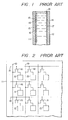
- Another such display device of conventional type has a structure as shown in Fig. 1.
- the device comprises a pair of transparent substrates of glass or the like facing each other.
- a spacer 13 is provided between the substrates 11 and 12 along the edges thereof.
- a liquid crystal 14 is sealed between the substrates 11 and 12.
- the substrates 11 and 12, spacer 13 and liquid crystal 14 constitute a liquid crystal cell.
- a plurality of display electrodes 15 consisting of a transparent conductive film are formed on the inner surface of one of the transparent substrates, i.e. substrate 11.
- thin film transistors 16 are formed as switching elements such that they are contiguous to the display electrodes 15 with their drains connected thereto.
- a common electrode 17 is formed on the other transparent substrate 12. The common electrode 17 faces the plurality of display electrodes 15.
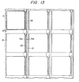
- the display electrodes 15 serve as picture element electrodes, for instance. As shown in Fig. 2, they are square in shape and arranged in a closely spaced-apart relation to one another. They are arranged in rows and columns on the transparent substrate 11. Gate buses 18 are formed such that they extend near and along the individual rows of display electrodes 15. Source buses 19 are formed such that they extend near and along the individual columns of display electrodes 15. The thin film transistors 16 noted above are formed at the intersections of the gate buses 18 and source buses 19. Each thin film transistor 16 has its gate connected to the associated gate bus 18, its source connected to the associated source bus 19 and its drain connected to the corresponding display electrode 15.
- the thin film transistor 16 has a structure as shown in Figs. 3 and 4.
- the display electrodes 15 and source buses 19 are formed from a transparent conductive film, e.g., an ITO, on the transparent substrate 11.
- a semiconductor layer 21 of amorphous silicon or the like is formed such that it strides parallel and closely spaced-apart portions of each display electrode 15 and the associated source bus 19.
- a gate insulating film 22 of silicon nitride or the like is formed on the semiconductor layer 21.
- a gate electrode 23 is formed on the gate insulating film 22 such that it overlies part of each display electrode 15 and associated source bus 19 via the gate insulating film 22 and each semiconductor layer 21. One end of the gate electrode 23 is connected to the associated gate bus 18.
- Portions of the display electrode 15 and source bus 19 facing each gate electrode 23 constitute drain and source electrodes 15a and 19a, respectively.
- the thin film transistor 16 is constituted by these electrodes 15a and 19a, the semiconductor layer 21, the gate insulating film 22 and the gate electrode 23.
- the individual gate electrodes 23 and gate buses 18 are formed simultaneously from aluminum, for instance.
- the semiconductor layer 21 is formed only over the region where the thin film transistor 16 is formed. Therefore, there is a considerable level difference between the gate electrode 23 and gate bus 18 with respect to the substrate 11. Due to this level difference, breakage of connection between the gate electrode 23 and gate bus 18 is liable to result.
- each of the semiconductor layer 21 and the gate insulating film 22 is formed over the entire surface other than the regions of display electrode 15 and source bus 19 in the same pattern as that of the contiguous gate bus 18 and gate electrode 23 to be formed.
- an aluminum layer, for instance, for the gate bus 18 and gate electrode 23 is formed over the two layers.
- a parasitic thin film transistor is formed by a portion (not shown) of the semiconductor layer 21 extending beneath the gate bus 18, gate insulating film 22, source bus 19 and drain electrode 15a.
- the amorphous silicon of the semiconductor layer 21 is photo-conductive, and its resistivity is reduced from 109 ⁇ -cm to about 104 ⁇ -cm when it is illuminated by light of 100,000 luxes. Therefore, when the semiconductor layer portion of the parasitic thin film transistor is illuminated, a current leak from the source bus 19 adjacent to the thin film transistor 16 is caused to deteriorate the on-off ratio thereof.
- a light-blocking layer 25 of chromium or like metal is formed such that it faces the semiconductor layer 21, as shown in Fig. 5.
- the light-blocking layer 25 is insulated from display electrode 15 and source bus 19 by an insulating layer 27. It may be thought to form the light-blocking layer 25 such that it faces the entire surface of the semiconductor layer portion to avoid the influence of the parasitic thin film transistor noted above. In this case, however, the electrostatic capacitance between the light-blocking layer and gate bus is increased too much to permit high speed control of the thin film transistor.
- the source bus terminal is constituted by the same material as the source bus, while the gate bus terminal is constituted by the same material as the gate bus.
- the source bus terminal is made of a transparent conductive material, e.g., ITO, while the gate bus terminal is made of aluminum. Since the two terminals are made of different materials, their connection to an external drive circuit requires different connection steps suited to these materials. The connection process, therefore, is rather cumbersome.
- the ITO constituting the source bus 19 has a comparatively low electric conductivity, that is, the source bus 19 has a comparatively high electric resistance. Therefore, a comparatively large difference in the drive voltage is produced between the opposite ends of the source bus 19. In other words, the transistors provided along the source bus can not be driven with a uniform voltage. This leads to a brightness slope in the screen of the liquid crystal display device according to the potential gradient along the source bus. It may be thought to increase the thickness of the source bus 19 to solve this problem. Doing so, however, would result in the precipitation of In during the formation of ITO by the plasma chemical vapor deposition process. The ITO film is thus denatured to deteriorate the characteristics of the thin film transistor. Further, since the source bus 19 is transparent, light leaks from portions of the source bus 19 which are not overlied by the transistors 16 and gate buses 18. This deteriorates the contrast of the displayed image.
- SID 84 Digest, 1984 discloses at page 308 a colour LCD addressed by a-Si thin-film transistors in which the gate electrode is narrower than the underlying a-Si.
- the gate insulating film extends substantially over the entire glass substrate, so that the gate electrode is completely isolated from the semiconductor layer and current leaks therefore cannot occur.
- An object of the invention is to provide a liquid crystal display device, which can be comparatively readily manufactured, can reduce the possibility of contamination of semiconductor layers in its manufacturing process, and has comparatively long surface distances of the source and drain electrodes from the gate electrode so that sufficient insulation can be maintained between these parts.
- Another object of the invention is to provide a liquid crystal display device, which can be readily connected to an external drive circuit.
- a further object of the invention is to provide a liquid crystal display device, with which a display image having high contrast can be obtained.
- a further object of the invention is to provide a liquid crystal display device, in which gate buses and gate electrodes have less level difference with respect to the associated substrate so that they are less liable to be broken and the on-off ratio of thin film transistors is high, and which is capable of high speed operation.
- a still further object of the invention is to provide a liquid crystal display device, in which the influence of parasitic transistors is reduced.
- the display device initially defined is characterized in that said gate insulating film has the same pattern as and perfectly overlies said semiconductor layer.
- the semiconductor layer and gate insulating film have extensions extending under the gate bus, and the gate bus and gate electrode have less level difference with respect to the associated transparent substrate so that they are less liable to be broken.
- a light-blocking layer may be formed such that it faces the semiconductor layer of the thin film transistor.
- the light-blocking layer may have an extension having an extra width on each side and extending to occupy the junction of the gate bus and corresponding gate electrode. The influence of the parasitic transistor is blocked by the extra width portion.
- the semiconductor layer and gate insulating layer have extensions extending under the gate bus, and the ratio L/W3 of the distance L between the gate bus and the nearest thin film transistor connected to the gate bus to the width W3 of the gate bus is set such that the current that flows from the nearest thin film transistor to the corresponding display electrode is higher by the order of one digit place or above than the current flowing from a parasitic transistor to the nearest thin film transistor on the side of the gate bus terminal to the display electrode.
- the ratio L/W3 is selected to be preferably higher than 4.5, for example.
- each of the source bus terminals is formed as a double-layered structure of a layer of the same material as that of the source buses and a layer of the same metal as the gate buses, the latter layer being formed on the former layer so that the portions of both the source bus terminals and the gate bus terminals can be directly connected to an external drive circuit.
- auxiliary conductive layers of the same material as the gate buses are formed on the source buses such that they are spaced apart from the gate buses and gate electrodes.
- the auxiliary conductive layers have an effect of reducing the resistance of the source buses, so that display having a uniform brightness can be obtained over the entire screen.
- the auxiliary conductive layers block light, so that substantially no light is transmitted at all time. Thus it is possible to obtain image display having a satisfactory contrast.
- amorphous silicon is used for the semiconductor layer of the thin film transistor, and a light-blocking layer of an amorphous silicon compound semiconductor having a smaller energy band gap than the energy band gap of amorphous silicon is formed such that it is contiguous to the semiconductor layer.
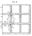
- Fig. 6 shows an embodiment of the liquid crystal display device according to the invention.
- This embodiment of device like the device described before in connection with Fig. 2, has display electrodes 15 arranged as picture element electrodes in rows and columns. Parts like those in Figs. 1 to 4 are designated by like reference numerals.
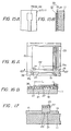
- Fig. 6 is a plan view similar to Fig. 3.
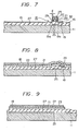
- Fig. 7 is a sectional view similar to Fig. 4, showing a thin film transistor 16.
- Fig. 8 is a sectional view taken along and showing a gate bus 18.
- Fig. 9 is a sectional view taken along and showing a channel region of the thin film transistor 16.
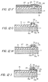
- Fig. 10 is a sectional view taken along and showing a gate bus. The structure shown in Figs. 6 through 10 will now be described with reference to Figs. 11 through 14 in the order of the steps of manufacture.
- each light-blocking layer 25 is formed on a portion of transparent substrate 11 between a region 15', which is to be occupied by a display electrode 15, and a region 19', which is to be occupied by a source bus 19.
- the light-blocking layer 25 overlies portions of regions 15a' and 19a' which are to serve as source and drain electrodes 15a and 19a, respectively.
- the light-blocking layer 25 is made of chromium, for instance and completely faces a so-called channel region of thin film transistor 16. In this embodiment, it extends into a region 26, which is to be occupied by a gate bus, to form a blocking portion 25a.
- the blocking portion 25a overlying the region 26 has extra width on each side with respect to the rest of it corresponding to the channel region.
- the film 28 will constitute the display electrodes 15 and source buses 19.
- the transparent conductive film 28 and ohmic contact layer 29 are then selectively photo-etched to form display electrodes 15, drain electrodes 15a, source buses 19 and source electrodes 19a, as shown in Figs. 7 to 10 and 13. At this time, the ohmic contact layer 29 remains on each display electrode 15 and source bus 19, as shown in Fig. 12E.
- a semiconductor layer 21 of amorphous silicon or the like is then formed on and over the entire surface of the wafer, as shown in Fig. 12F.
- a gate insulating film 22, e.g., a silicon nitride film, is formed on the semiconductor film 21.
- the semiconductor layer 21 and gate insulating film 22 are then selectively photo-etched to leave those regions constituting the thin film transistors 16, i.e. the regions striding across the opposing marginal edges of the display electrodes 15 and the source buses 19, and also those regions corresponding to the gate buses 18 but being slightly wider than them.
- the portions of the photo-etched semiconductor layer 21 left above the blocking portions 25a of the light-blocking layer 25 have a width W2 which is slightly larger than the width W1 of the portions 25a photo-etched semiconductor layer 21 left as parts of the thin film transistors as shown in Fig. 14.
- the ohmic contact layer 29 over the display electrodes 15 and source buses 19 is removed except for portions over the drain and source electrodes 15a and 19a.
- the semiconductor layer 21 and gate insulating film 22 are patterned with entirely the same pattern so that they perfectly overlie each other.
- the semiconductor layer 21 is in ohmic contact with the drain and source electrodes 15a and 19a via the ohmic contact layer 29.
- a metal layer e.g., an aluminum layer 31, which will constitute the gate electrodes, is formed as shown in Fig. 12H.
- This layer is then selectively photo-etched to form the gate electrodes 23 and gate buses 18, as shown in Figs. 6 to 10. This patterning is done such that the edges of the gate electrode 23 and gate bus 18 are not flush with the corresponding edges of the patterned gate insulating film 22 but are inwardly spaced apart therefrom by a slight distance d, e.g., 2 to 3 ⁇ m or above as shown in Figs. 6, 7 and 10.
- auxiliary conductive layers 32 are preferably formed from an aluminum layer 31 on the source buses 19 each to extend along one side of the adjacent display electrode 15 between adjacent two gate buses 18, as shown in Figs. 6 and 7. That is, the source bus 19 preferably has a double-layer structure. It is also preferable to form source bus terminals 33 in a similar double-layer structure as shown in Figs. 15A and 15B, where each source bus terminal 33 consists of a layer 19 of the same material (e.g. ITO) as the source bus 19 and an auxiliary conductive layer 32.
- ITO the same material
- L/W3 is set to 4.5 or above.
- the end of the semiconductor layer portion 21a extending underneath the gate bus 18 is connected to the gate bus terminal 38, and a sort of parasitic FET is formed by the gate bus terminal 38 as the source along with the drain electrode 15a, semiconductor layer 21a and gate bus 18.
- the afore-mentioned ratio L/W3 is set such that the current that flows from channel of the thin film transistor 16 to the display electrode 15 is higher by the order of one digit place or above than the current flowing from the parasitic FET to the display electrode 15.
- a passivation film 35 consisting of a transparent insulating film, e.g., of silicon nitride, polyimide, etc., is formed over the entire surface, as shown in Fig. 12I.
- the passivation film 35 prevents direct contact of the thin film transistors 16 with the liquid crystal 14. Thus, it improves the stability. In addition, it reduces leak current between the gate 23 and source and drain electrodes 19a and 15a.
- the semiconductor layer 21 and gate insulating film 22 are formed under the entirety of the gate electrode 23 of each thin film transistor 16 and each gate bus 18.
- the difference in level between the gate electrode 23 and the gate bus 18 with respect to the substrate 11 is reduced that much to reduce the possibility of breakage of the connection between the gate electrode 23 and the gate bus 18.
- the possibility of short-circuit between the gate and the source buses 18 and 19 is reduced by the presence of the two layers, i.e., the semiconductor layer 21 and the gate insulating film 22, between these buses 18 and 19.
- the side edges of the gate electrode 23 and gate bus 18 are spaced apart inwardly, by the distance d in Fig. 7, from the corresponding side edges of the gate insulating film 22.
- the surface distance of the drain or source electrode 15a or 19a from the gate electrode 23 is increased that much to reduce the possibility of current leak between these electrodes.
- the gate insulating film 22 and semiconductor layer 21 has the same pattern and perfectly over lie each other. Since these two layers are patterned simultaneously, the possibility of contamination between these two layers is reduced.
- the auxiliary conductive layer 32 is formed on the source bus 19 as described above, the thickness of the source bus is increased that much to reduce the possibility of breakage of the bus. In addition, the electric resistance is reduced. Besides, the auxiliary conductive layer 32 is formed simultaneously with the formation of the gate electrode 23 and does not require any additional step of manufacture. Moreover, the double-layer structure of the source bus terminal 33 consisting of the material of the source bus 19 and the auxiliary conductive layer 32 as described before in connection with Figs. 15A and 15B, has a further advantage.
- the surface of the source bus terminal 33, which is to be connected to the external part, is constituted by the same material as the gate bus terminal 38. Thus, the source and gate bus terminals can be connected simultaneously and under the same conditions to an external drive circuit by means of thermal press or soldering, which is very convenient.
- the light-blocking layer 25 with the extra width portion 25a is provided.
- the semiconductor layer portion 21a extending underneath the gate bus 18 undergoes a resistance reduction when it receives external light, i.e., ambient external light or illumination light.
- the extra width portion 25a substantially eliminates such current increase.
- the extra width portion 25a eliminates the interaction between the semiconductor layer portion 21a underneath the gate bus 18 and the channel portion of the thin film transistor 16. If the light-blocking layer 25 is formed underneath the entire length of each gate bus 18, the increase of the current when the thin film transistors 16 are turned off can be significantly reduced. In this case, however, a large electrostatic capacitance is formed between the light-blocking layer 25 and gate bus 18, and coupled to the gate electrode 23, which is undesired.
- the source buses 19 are constituted by a transparent conductive film, which has a comparatively high resistance. If it is intended to reduce the resistance of each source bus 19 by increasing the thickness thereof, the manufacturing process is extended. In addition, deterioration of the thin film transistor characteristics due to denaturing is liable to result. Since the source buses 19 are transparent, the liquid crystal display device can transmit light in the regions of the source buses 19 at all time. The contrast of the displayed image is thus correspondingly deteriorated.
- the auxiliary conductive layer 32 blocks light and can improve the contrast that much. In addition, it reduces the resistance of each source bus 19. This has an effect of improving the uniformity of brightness of the image display on the display device.
- the passivation film 35 eliminates mutual adverse effects of the liquid crystal 14 and thin film transistors 16. In addition, it reduces the possibility of such fault as a short-circuit between buses due to rubbing. Further, it can block any residual DC component of a liquid crystal drive signal waveform, i.e., it will prevent such DC component from being applied across the liquid crystal 14.
- the light-blocking layer 25 has been made of a metal.
- Fig. 17 shows an instance, which uses a non-metal light-blocking layer.
- the non-metal light-blocking layer 25' is formed on transparent substrate 11, and a semiconductor layer 21 of amorphous silicon is formed on the layer 25'.
- light-blocking layer 25', semiconductor layer 21, gate insulating film 22 and gate electrode 23 are formed by simultaneous selective photo-etching patterning using the same mask.
- display electrode 15 and source bus 19 are formed directly on the substrate 11 such that they have edges contiguous to corresponding edges of the display electrode 15 and source bus 19.
- an insulating layer capable of blocking sodium ions may be formed on transparent substrate 11, and display electrode 15, source bus 19 and light-blocking layer 25' may be formed on the insulating layer.
- the light-blocking layer 25' of this example is made of a compound semiconductor containing amorphous silicon.
- This compound semiconductor has a narrower energy band gap and no less resistivity than those of the amorphous silicon constituting the semiconductor layer 21.
- compound semiconductors as amorphous silicon germanium and amorphous silicon tin may be used.
- the energy band gap of these compound semiconductors is 1.0 to 1.7 electron volts, which is narrower than that of the amorphous silicon semiconductor layer 21, namely 1.7 to 20 electron volts.
- the light-blocking layer 25' may be formed using a so-called plasma chemical vapor deposition process.
- a binary compound semiconductor layer of amorphous silicon germanium may be obtained by using SiH and GeH gases as sources of components and by suitably controlling their mole ratio.
- the layer thus formed contains silicon and germanium in atomic weight proportions of about 0.8 : 0.2. These proportions may be suitably varied by appropriately selecting the mole ratio of the vapor growth. Usually, germanium is contained more than the ratio of 0.8 : 0.2 noted above.
- a binary compound semiconductor of amorphous silicon tin may be obtained by suitably selecting the mole ratio of SiH4 and Sn(CH3)4, i.e., by controlling the gas flow.
- a resistivity of 108 to 1012 ⁇ -cm which is substantially the same as the resistivity of the amorphous silicon semiconductor layer 21. It is possible to form first a layer of amorphous silicon germanium or amorphous silicon tin as the light-blocking layer and continually form an amorphous silicon layer, i.e., the semiconductor layer 21.
- the amorphous silicon compound semiconductor light-blocking layer is free from the problems of the electrostatic capacitance and insulation between it and the display electrode and source bus. In addition, it can be readily formed.
- the light-blocking layer 25' may be omitted.
- the display electrodes 15 are not limited to the picture element electrodes and may be used in other forms as well. For example, seven display electrodes may be arranged as respective segments of a figure eight and selectively driven for the display of a figure.
Abstract
Description
- This invention relates to a liquid crystal display device comprising: a liquid crystal cell including first and second transparent substrates spaced apart a small distance and facing each other and a liquid crystal sealed between said first and second transparent substrates; a common electrode constituted by a transparent conductive film formed on the inner surface of said first transparent substrate; a plurality of display electrodes constituted by a transparent conductive film formed on the inner surface of said second transparent substrate; a plurality of thin film transistors having respective drains connected to respective ones of the said plurality of display electrodes; each of said thin film transistors including: a drain electrode constituted by a portion of said display electrode; a source electrode electrically connected to a corresponding source bus; a semiconductor layer provided between and overlying said drain and source electrodes; a gate insulating film overlying said semiconductor layer; and a gate electrode connected to a corresponding gate bus and formed on said gate insulating film, an edge of said gate electrode being spaced back from the corresponding edge of said gate insulating film, so that the gate electrode only partly overlies said gate insulating film.
- Such a device is described in "A 7.23-in. Diagonal Color LCD Addressed by a-Si TFTs" by Ugai et al published in 1984 SID Digest, page 308.
- Such a device is employable for displaying an image, for instance, and may constitute an active matrix type liquid crystal display device, that has a plurality of display electrodes provided in a liquid crystal cell and selectively drivable by thin film transistors for display.
- A prior art liquid crystal display device is disclosed in "Electronics International", May 19, 1982 at page 94. Another such display device of conventional type has a structure as shown in Fig. 1. The device comprises a pair of transparent substrates of glass or the like facing each other. A
spacer 13 is provided between thesubstrates liquid crystal 14 is sealed between thesubstrates substrates spacer 13 andliquid crystal 14 constitute a liquid crystal cell. A plurality ofdisplay electrodes 15 consisting of a transparent conductive film are formed on the inner surface of one of the transparent substrates, i.e.substrate 11. Alsothin film transistors 16 are formed as switching elements such that they are contiguous to thedisplay electrodes 15 with their drains connected thereto. Acommon electrode 17 is formed on the othertransparent substrate 12. Thecommon electrode 17 faces the plurality ofdisplay electrodes 15. - The
display electrodes 15 serve as picture element electrodes, for instance. As shown in Fig. 2, they are square in shape and arranged in a closely spaced-apart relation to one another. They are arranged in rows and columns on thetransparent substrate 11.Gate buses 18 are formed such that they extend near and along the individual rows ofdisplay electrodes 15.Source buses 19 are formed such that they extend near and along the individual columns ofdisplay electrodes 15. Thethin film transistors 16 noted above are formed at the intersections of thegate buses 18 andsource buses 19. Eachthin film transistor 16 has its gate connected to the associatedgate bus 18, its source connected to the associatedsource bus 19 and its drain connected to thecorresponding display electrode 15. - When one of the
gate buses 18 and one of thesource buses 19 are selected, a voltage is applied between the selected buses. As a result, only the correspondingthin film transistor 16 is turned on. Charge is stored on thedisplay electrode 15 connected to the drain of the "on"thin film transistor 16. A voltage is applied across only a portion of theliquid crystal 14 between thisdisplay electrode 15 and thecommon electrode 17. Only thisdisplay electrode 15 is thus rendered transparent or opaque. In this way, only selected display electrodes are driven for display. Actually, selected display electrodes are usually rendered transparent or opaque in combination with a polarizer (not shown). - Usually, the
thin film transistor 16 has a structure as shown in Figs. 3 and 4. Referring to these Figures, thedisplay electrodes 15 andsource buses 19 are formed from a transparent conductive film, e.g., an ITO, on thetransparent substrate 11. Asemiconductor layer 21 of amorphous silicon or the like is formed such that it strides parallel and closely spaced-apart portions of eachdisplay electrode 15 and the associatedsource bus 19. Agate insulating film 22 of silicon nitride or the like is formed on thesemiconductor layer 21. Agate electrode 23 is formed on thegate insulating film 22 such that it overlies part of eachdisplay electrode 15 and associatedsource bus 19 via thegate insulating film 22 and eachsemiconductor layer 21. One end of thegate electrode 23 is connected to the associatedgate bus 18. Portions of thedisplay electrode 15 andsource bus 19 facing eachgate electrode 23 constitute drain andsource electrodes thin film transistor 16 is constituted by theseelectrodes semiconductor layer 21, the gateinsulating film 22 and thegate electrode 23. Theindividual gate electrodes 23 andgate buses 18 are formed simultaneously from aluminum, for instance. - In the above prior art structure, the
semiconductor layer 21 is formed only over the region where thethin film transistor 16 is formed. Therefore, there is a considerable level difference between thegate electrode 23 andgate bus 18 with respect to thesubstrate 11. Due to this level difference, breakage of connection between thegate electrode 23 andgate bus 18 is liable to result. - Accordingly, it has been proposed to form the
semiconductor layer 21 and thegate insulating film 22 such that each of them has the same pattern as that of thegate electrode 23 andgate bus 18, as shown in Fig. 5. More specifically, in this proposal each of thesemiconductor layer 21 and gateinsulating film 22 is formed over the entire surface other than the regions ofdisplay electrode 15 andsource bus 19 in the same pattern as that of thecontiguous gate bus 18 andgate electrode 23 to be formed. Then an aluminum layer, for instance, for thegate bus 18 andgate electrode 23, is formed over the two layers. With this structure, the level difference between thegate bus 18 andgate electrode 23 with respect to thesubstrate 11 is reduced to reduce the possibility of breakage of connection. In this case, however, the surface distance (i.e. distance along the surface) between thegate electrode 23 and thesource electrode 19a and that between thegate electrode 23 anddrain electrode 15a are reduced, leading to the problems of current leaks between these parts. - Further, with the structure noted above a parasitic thin film transistor is formed by a portion (not shown) of the
semiconductor layer 21 extending beneath thegate bus 18, gateinsulating film 22,source bus 19 anddrain electrode 15a. The amorphous silicon of thesemiconductor layer 21 is photo-conductive, and its resistivity is reduced from 10⁹Ω-cm to about 10⁴Ω-cm when it is illuminated by light of 100,000 luxes. Therefore, when the semiconductor layer portion of the parasitic thin film transistor is illuminated, a current leak from thesource bus 19 adjacent to thethin film transistor 16 is caused to deteriorate the on-off ratio thereof. - In order to prevent deterioration of the on-off ratio of the
thin film transistor 16 with the illumination of thesemiconductor layer 21 thereof, a light-blockinglayer 25 of chromium or like metal is formed such that it faces thesemiconductor layer 21, as shown in Fig. 5. In this case, the light-blockinglayer 25 is insulated fromdisplay electrode 15 andsource bus 19 by aninsulating layer 27. It may be thought to form the light-blockinglayer 25 such that it faces the entire surface of the semiconductor layer portion to avoid the influence of the parasitic thin film transistor noted above. In this case, however, the electrostatic capacitance between the light-blocking layer and gate bus is increased too much to permit high speed control of the thin film transistor. - To reduce the electrostatic capacitance between the light-blocking
layer 25 and drain andsource electrodes layer 25 and gate bus, it may be thought to increase the thickness of theinsulating layer 27. Doing so, however, requires increased time for manufacture and deteriorates the yield. - In a further aspect, the source bus terminal is constituted by the same material as the source bus, while the gate bus terminal is constituted by the same material as the gate bus. For example, the source bus terminal is made of a transparent conductive material, e.g., ITO, while the gate bus terminal is made of aluminum. Since the two terminals are made of different materials, their connection to an external drive circuit requires different connection steps suited to these materials. The connection process, therefore, is rather cumbersome.
- Further, the ITO constituting the
source bus 19 has a comparatively low electric conductivity, that is, thesource bus 19 has a comparatively high electric resistance. Therefore, a comparatively large difference in the drive voltage is produced between the opposite ends of thesource bus 19. In other words, the transistors provided along the source bus can not be driven with a uniform voltage. This leads to a brightness slope in the screen of the liquid crystal display device according to the potential gradient along the source bus. It may be thought to increase the thickness of thesource bus 19 to solve this problem. Doing so, however, would result in the precipitation of In during the formation of ITO by the plasma chemical vapor deposition process. The ITO film is thus denatured to deteriorate the characteristics of the thin film transistor. Further, since thesource bus 19 is transparent, light leaks from portions of thesource bus 19 which are not overlied by thetransistors 16 andgate buses 18. This deteriorates the contrast of the displayed image. - SID 84 Digest, 1984 discloses at page 308 a colour LCD addressed by a-Si thin-film transistors in which the gate electrode is narrower than the underlying a-Si. Here the gate insulating film extends substantially over the entire glass substrate, so that the gate electrode is completely isolated from the semiconductor layer and current leaks therefore cannot occur.
- An object of the invention is to provide a liquid crystal display device, which can be comparatively readily manufactured, can reduce the possibility of contamination of semiconductor layers in its manufacturing process, and has comparatively long surface distances of the source and drain electrodes from the gate electrode so that sufficient insulation can be maintained between these parts.
- Another object of the invention is to provide a liquid crystal display device, which can be readily connected to an external drive circuit.
- A further object of the invention is to provide a liquid crystal display device, with which a display image having high contrast can be obtained.
- A further object of the invention is to provide a liquid crystal display device, in which gate buses and gate electrodes have less level difference with respect to the associated substrate so that they are less liable to be broken and the on-off ratio of thin film transistors is high, and which is capable of high speed operation.
- A still further object of the invention is to provide a liquid crystal display device, in which the influence of parasitic transistors is reduced.
- According to the invention, the display device initially defined is characterized in that said gate insulating film has the same pattern as and perfectly overlies said semiconductor layer.
- According to one embodiment of the invention, the semiconductor layer and gate insulating film have extensions extending under the gate bus, and the gate bus and gate electrode have less level difference with respect to the associated transparent substrate so that they are less liable to be broken. In addition, a light-blocking layer may be formed such that it faces the semiconductor layer of the thin film transistor. The light-blocking layer may have an extension having an extra width on each side and extending to occupy the junction of the gate bus and corresponding gate electrode. The influence of the parasitic transistor is blocked by the extra width portion.
- According to a further embodiment of the invention, the semiconductor layer and gate insulating layer have extensions extending under the gate bus, and the ratio L/W₃ of the distance L between the gate bus and the nearest thin film transistor connected to the gate bus to the width W₃ of the gate bus is set such that the current that flows from the nearest thin film transistor to the corresponding display electrode is higher by the order of one digit place or above than the current flowing from a parasitic transistor to the nearest thin film transistor on the side of the gate bus terminal to the display electrode. The ratio L/W₃ is selected to be preferably higher than 4.5, for example.
- According to another embodiment of the invention, each of the source bus terminals is formed as a double-layered structure of a layer of the same material as that of the source buses and a layer of the same metal as the gate buses, the latter layer being formed on the former layer so that the portions of both the source bus terminals and the gate bus terminals can be directly connected to an external drive circuit.
- According to a further embodiment of the invention, auxiliary conductive layers of the same material as the gate buses are formed on the source buses such that they are spaced apart from the gate buses and gate electrodes. The auxiliary conductive layers have an effect of reducing the resistance of the source buses, so that display having a uniform brightness can be obtained over the entire screen. In addition, the auxiliary conductive layers block light, so that substantially no light is transmitted at all time. Thus it is possible to obtain image display having a satisfactory contrast.
- According to a still further embodiment of the invention, amorphous silicon is used for the semiconductor layer of the thin film transistor, and a light-blocking layer of an amorphous silicon compound semiconductor having a smaller energy band gap than the energy band gap of amorphous silicon is formed such that it is contiguous to the semiconductor layer.
- Further, the features noted above may be combined.
- For a better understanding of the invention, and to show the same may be carried into effect, reference will now be made, by way of example, to the accompanying drawings, in which:-
- Fig. 1 is a fragmentary sectional view showing a usual liquid crystal display device;
- Fig. 2 is a circuit diagram showing an electric circuit of display electrodes and thin film transistors of the liquid crystal display device shown in Fig. 1;
- Fig. 3 is a fragmentary plan view
showing display electrodes 15 andthin film transistors 16 in the prior art structure shown in Fig. 2; - Fig. 4 is a sectional view taken along line 101-101 in Fig. 3;
- Fig. 5 is a sectional view showing a prior art thin film transistor with a light-blocking layer;
- Fig. 6 is a fragmentary plan view similar to Fig. 3 but showing a main portion of a liquid crystal display device according to the invention;
- Fig. 7 is a sectional view taken along line 102-102 in Fig. 6;
- Fig. 8 is a sectional view taken along line 103-103 in Fig. 6;
- Fig. 9 is a sectional view taken along line 104-104 in Fig. 6;
- Fig. 10 is a sectional view taken along line 105-105 in Fig. 6;
- Fig. 11 is a fragmentary plan view showing an arrangement with light-blocking
layers 25 formed on a transparent substrate; - Figs. 12A to 12I are sectional views illustrating a process of manufacture of the display electrodes and thin film transistors shown in Fig. 6;
- Fig. 13 is a fragmentary sectional view showing display electrodes and source buses;
- Fig. 14 is a fragmentary plan view showing semiconductor layers;
- Figs. 15A and 15B are a fragmentary plan view and a fragmentary sectional view, respectively, showing a source bus terminal;
- Figs. 16A and 16B are a fragmentary plan view and a fragmentary sectional view, respectively, showing a gate bus terminal; and
- Fig. 17 is a fragmentary sectional view showing a thin film transistor with a light-blocking
layer 25 continuous to asemiconductor layer 21. - Fig. 6 shows an embodiment of the liquid crystal display device according to the invention. This embodiment of device, like the device described before in connection with Fig. 2, has
display electrodes 15 arranged as picture element electrodes in rows and columns. Parts like those in Figs. 1 to 4 are designated by like reference numerals. - Fig. 6 is a plan view similar to Fig. 3. Fig. 7 is a sectional view similar to Fig. 4, showing a
thin film transistor 16. Fig. 8 is a sectional view taken along and showing agate bus 18. Fig. 9 is a sectional view taken along and showing a channel region of thethin film transistor 16. Fig. 10 is a sectional view taken along and showing a gate bus. The structure shown in Figs. 6 through 10 will now be described with reference to Figs. 11 through 14 in the order of the steps of manufacture. - In this embodiment, light-blocking layers are formed. More specifically, as shown in Figs. 11 and 12A, each light-blocking
layer 25 is formed on a portion oftransparent substrate 11 between a region 15', which is to be occupied by adisplay electrode 15, and a region 19', which is to be occupied by asource bus 19. The light-blockinglayer 25 overlies portions ofregions 15a' and 19a' which are to serve as source anddrain electrodes layer 25 is made of chromium, for instance and completely faces a so-called channel region ofthin film transistor 16. In this embodiment, it extends into aregion 26, which is to be occupied by a gate bus, to form a blockingportion 25a. The blockingportion 25a overlying theregion 26 has extra width on each side with respect to the rest of it corresponding to the channel region. - Subsequently, an insulating
layer 27 of silicon dioxide, for instance, is formed over the entire surface of thetransparent substrate 11, as shown in Figs. 7 to 10 and 12B. A transparentconductive film 28, of ITO for instance, is then formed on and over the entire surface of the insulatingfilm 27. Thefilm 28 will constitute thedisplay electrodes 15 andsource buses 19. Anohmic contact layer 29, of n⁺-type amorphous silicon for instance, is then formed on and over the entire surface of the transparentconductive film 28, as shown in Fig. 12D, so that ohmic contact with the semiconductor layer can be reliably obtained. The transparentconductive film 28 andohmic contact layer 29 are then selectively photo-etched to formdisplay electrodes 15,drain electrodes 15a,source buses 19 andsource electrodes 19a, as shown in Figs. 7 to 10 and 13. At this time, theohmic contact layer 29 remains on eachdisplay electrode 15 andsource bus 19, as shown in Fig. 12E. - A
semiconductor layer 21 of amorphous silicon or the like is then formed on and over the entire surface of the wafer, as shown in Fig. 12F. Agate insulating film 22, e.g., a silicon nitride film, is formed on thesemiconductor film 21. Thesemiconductor layer 21 andgate insulating film 22 are then selectively photo-etched to leave those regions constituting thethin film transistors 16, i.e. the regions striding across the opposing marginal edges of thedisplay electrodes 15 and thesource buses 19, and also those regions corresponding to thegate buses 18 but being slightly wider than them. The portions of the photo-etchedsemiconductor layer 21 left above the blockingportions 25a of the light-blockinglayer 25 have a width W₂ which is slightly larger than the width W₁ of theportions 25a photo-etchedsemiconductor layer 21 left as parts of the thin film transistors as shown in Fig. 14. At the time of the selective photo-etching patterning of thegate insulating film 22 andsemiconductor layer 21, theohmic contact layer 29 over thedisplay electrodes 15 andsource buses 19 is removed except for portions over the drain andsource electrodes semiconductor layer 21 andgate insulating film 22 are patterned with entirely the same pattern so that they perfectly overlie each other. Thesemiconductor layer 21 is in ohmic contact with the drain andsource electrodes ohmic contact layer 29. - Subsequently, a metal layer, e.g., an
aluminum layer 31, which will constitute the gate electrodes, is formed as shown in Fig. 12H. This layer is then selectively photo-etched to form thegate electrodes 23 andgate buses 18, as shown in Figs. 6 to 10. This patterning is done such that the edges of thegate electrode 23 andgate bus 18 are not flush with the corresponding edges of the patternedgate insulating film 22 but are inwardly spaced apart therefrom by a slight distance d, e.g., 2 to 3 µm or above as shown in Figs. 6, 7 and 10. Further, auxiliaryconductive layers 32 are preferably formed from analuminum layer 31 on thesource buses 19 each to extend along one side of theadjacent display electrode 15 between adjacent twogate buses 18, as shown in Figs. 6 and 7. That is, thesource bus 19 preferably has a double-layer structure. It is also preferable to formsource bus terminals 33 in a similar double-layer structure as shown in Figs. 15A and 15B, where eachsource bus terminal 33 consists of alayer 19 of the same material (e.g. ITO) as thesource bus 19 and an auxiliaryconductive layer 32. - Further, at a terminal 38 of each
gate bus 18, as shown in Figs. 16A and 16B, denoting the width of thegate bus 18 by W₃ and the distance between the end of thegate insulating film 22 andsource electrode 19a under thegate bus 18 by L, L/W₃ is set to 4.5 or above. With the structure of this embodiment, the end of the semiconductor layer portion 21a extending underneath thegate bus 18 is connected to thegate bus terminal 38, and a sort of parasitic FET is formed by thegate bus terminal 38 as the source along with thedrain electrode 15a, semiconductor layer 21a andgate bus 18. The afore-mentioned ratio L/W₃ is set such that the current that flows from channel of thethin film transistor 16 to thedisplay electrode 15 is higher by the order of one digit place or above than the current flowing from the parasitic FET to thedisplay electrode 15. - After the
thin film transistors 16 have been formed, apassivation film 35 consisting of a transparent insulating film, e.g., of silicon nitride, polyimide, etc., is formed over the entire surface, as shown in Fig. 12I. Thepassivation film 35 prevents direct contact of thethin film transistors 16 with theliquid crystal 14. Thus, it improves the stability. In addition, it reduces leak current between thegate 23 and source anddrain electrodes - As has been shown, with the liquid crystal display device according to the invention the
semiconductor layer 21 andgate insulating film 22 are formed under the entirety of thegate electrode 23 of eachthin film transistor 16 and eachgate bus 18. Thus, the difference in level between thegate electrode 23 and thegate bus 18 with respect to thesubstrate 11 is reduced that much to reduce the possibility of breakage of the connection between thegate electrode 23 and thegate bus 18. In addition, the possibility of short-circuit between the gate and thesource buses semiconductor layer 21 and thegate insulating film 22, between thesebuses - Further, according to the invention the side edges of the
gate electrode 23 andgate bus 18 are spaced apart inwardly, by the distance d in Fig. 7, from the corresponding side edges of thegate insulating film 22. Thus, the surface distance of the drain orsource electrode gate electrode 23 is increased that much to reduce the possibility of current leak between these electrodes. Further, thegate insulating film 22 andsemiconductor layer 21 has the same pattern and perfectly over lie each other. Since these two layers are patterned simultaneously, the possibility of contamination between these two layers is reduced. - Further, where the auxiliary
conductive layer 32 is formed on thesource bus 19 as described above, the thickness of the source bus is increased that much to reduce the possibility of breakage of the bus. In addition, the electric resistance is reduced. Besides, the auxiliaryconductive layer 32 is formed simultaneously with the formation of thegate electrode 23 and does not require any additional step of manufacture. Moreover, the double-layer structure of thesource bus terminal 33 consisting of the material of thesource bus 19 and the auxiliaryconductive layer 32 as described before in connection with Figs. 15A and 15B, has a further advantage. The surface of thesource bus terminal 33, which is to be connected to the external part, is constituted by the same material as thegate bus terminal 38. Thus, the source and gate bus terminals can be connected simultaneously and under the same conditions to an external drive circuit by means of thermal press or soldering, which is very convenient. - Further, according to the invention the light-blocking
layer 25 with theextra width portion 25a is provided. The semiconductor layer portion 21a extending underneath thegate bus 18 undergoes a resistance reduction when it receives external light, i.e., ambient external light or illumination light. Unless theextra width portion 25a is provided, a current increase would result from the resistance reduction at the time when thethin film transistor 16 is turned off. Theextra width portion 25a substantially eliminates such current increase. In other words, theextra width portion 25a eliminates the interaction between the semiconductor layer portion 21a underneath thegate bus 18 and the channel portion of thethin film transistor 16. If the light-blockinglayer 25 is formed underneath the entire length of eachgate bus 18, the increase of the current when thethin film transistors 16 are turned off can be significantly reduced. In this case, however, a large electrostatic capacitance is formed between the light-blockinglayer 25 andgate bus 18, and coupled to thegate electrode 23, which is undesired. - The
source buses 19 are constituted by a transparent conductive film, which has a comparatively high resistance. If it is intended to reduce the resistance of eachsource bus 19 by increasing the thickness thereof, the manufacturing process is extended. In addition, deterioration of the thin film transistor characteristics due to denaturing is liable to result. Since thesource buses 19 are transparent, the liquid crystal display device can transmit light in the regions of thesource buses 19 at all time. The contrast of the displayed image is thus correspondingly deteriorated. The auxiliaryconductive layer 32, however, blocks light and can improve the contrast that much. In addition, it reduces the resistance of eachsource bus 19. This has an effect of improving the uniformity of brightness of the image display on the display device. - The
passivation film 35 eliminates mutual adverse effects of theliquid crystal 14 andthin film transistors 16. In addition, it reduces the possibility of such fault as a short-circuit between buses due to rubbing. Further, it can block any residual DC component of a liquid crystal drive signal waveform, i.e., it will prevent such DC component from being applied across theliquid crystal 14. - In the above embodiment, the light-blocking
layer 25 has been made of a metal. However, it is possible to provide light-blocking layers made of materials other than metals, e.g., black ink, a light-blocking insulating film or a compound semiconductor composed of amorphous silicon and a light-absorbing metal. - Fig. 17 shows an instance, which uses a non-metal light-blocking layer. In this instance, the non-metal light-blocking layer 25' is formed on
transparent substrate 11, and asemiconductor layer 21 of amorphous silicon is formed on the layer 25'. In this example, light-blocking layer 25',semiconductor layer 21,gate insulating film 22 and gate electrode 23 (gate bus 18) are formed by simultaneous selective photo-etching patterning using the same mask. Subsequently,display electrode 15 andsource bus 19 are formed directly on thesubstrate 11 such that they have edges contiguous to corresponding edges of thedisplay electrode 15 andsource bus 19. As an alternative to this example, an insulating layer capable of blocking sodium ions may be formed ontransparent substrate 11, anddisplay electrode 15,source bus 19 and light-blocking layer 25' may be formed on the insulating layer. - The light-blocking layer 25' of this example is made of a compound semiconductor containing amorphous silicon. This compound semiconductor has a narrower energy band gap and no less resistivity than those of the amorphous silicon constituting the
semiconductor layer 21. For example, such compound semiconductors as amorphous silicon germanium and amorphous silicon tin may be used. The energy band gap of these compound semiconductors is 1.0 to 1.7 electron volts, which is narrower than that of the amorphoussilicon semiconductor layer 21, namely 1.7 to 20 electron volts. - The light-blocking layer 25' may be formed using a so-called plasma chemical vapor deposition process. A binary compound semiconductor layer of amorphous silicon germanium may be obtained by using SiH and GeH gases as sources of components and by suitably controlling their mole ratio. The layer thus formed contains silicon and germanium in atomic weight proportions of about 0.8 : 0.2. These proportions may be suitably varied by appropriately selecting the mole ratio of the vapor growth. Usually, germanium is contained more than the ratio of 0.8 : 0.2 noted above. A binary compound semiconductor of amorphous silicon tin may be obtained by suitably selecting the mole ratio of SiH₄ and Sn(CH₃)₄, i.e., by controlling the gas flow. In either case, it is possible to obtain a resistivity of 10⁸ to 10¹² Ω-cm, which is substantially the same as the resistivity of the amorphous
silicon semiconductor layer 21. It is possible to form first a layer of amorphous silicon germanium or amorphous silicon tin as the light-blocking layer and continually form an amorphous silicon layer, i.e., thesemiconductor layer 21. - The amorphous silicon compound semiconductor light-blocking layer is free from the problems of the electrostatic capacitance and insulation between it and the display electrode and source bus. In addition, it can be readily formed.
- The light-blocking layer 25', however, may be omitted. Further, the
display electrodes 15 are not limited to the picture element electrodes and may be used in other forms as well. For example, seven display electrodes may be arranged as respective segments of a figure eight and selectively driven for the display of a figure.
Claims (14)
- A liquid crystal display device comprising:
a liquid crystal cell including first and second transparent substrates (11, 12) spaced apart a small distance and facing each other and a liquid crystal (14) sealed between said first and second transparent substrates (11, 12);
a common electrode (17) constituted by a transparent conductive film formed on the inner surface of said first transparent substrate (12);
a plurality of display electrodes (15) constituted by a transparent conductive film formed on the inner surface of said second transparent substrate (11);
a plurality of thin film transistors (16) having respective drains connected to respective ones of the said plurality of display electrodes (15);
each of said thin film transistors (16) including:
a drain electrode (15a) constituted by a portion of said display electrode;
a source electrode (19a) electrically connected to a corresponding source bus (19);
a semiconductor layer (21) provided between and overlying said drain and source electrodes (15a, 19a);
a gate insulating film (22) overlying said semiconductor layer (21); and
a gate electrode (23) connected to a corresponding gate bus (18) and formed on said gate insulating film (22), an edge of said gate electrode (23) being spaced back from the corresponding edge of said gate insulating film (22), so that the gate electrode only partly overlies said gate insulating film,
characterized in that:
said gate insulating film (22) has the same pattern as and perfectly overlies said semiconductor layer (21). - A liquid crystal display device according to claim 1 wherein auxiliary conductive layers (32) are formed on said source buses from the same material as said gate buses and spaced apart from said gate electrodes and said gate buses.
- A liquid crystal display device according to claim 1 or 2 wherein said source buses (19) have terminals each constituted by a lamination of a first layer of the same material as said source buses and a second layer of the same material as said gate bus.
- A liquid crystal display device according to any one of claims 1 to 3 wherein said semiconductor layer (21) and gate insulating film (22) have extensions (21a) provided underneath said gate bus (18).
- A liquid crystal display device according to claim 4 further comprising a parasitic transistor being formed by said drain electrode (15a), said semiconductor extension layer (21a) and said gate bus (18),
wherein the ratio L/W₃ is selected such that the current which flows from the nearest thin film transistor to the corresponding display electrode is higher by at least an order of magnitude than the current flowing via said parasitic transistor to said display electrode, where L is the distance from one end of each said extension to the nearest thin film transistor connected to said gate bus, and W₃ is the width of said gate bus. - A liquid crystal display device according to claim 5 wherein said ratio L/W₃ is 4.5 or above.
- A liquid crystal display device according to any preceding claim further comprising:
light-blocking layers (25) each formed on said second transparent substrate and each facing a respective said thin film transistors (16) above thereof. - A liquid crystal display device according to claim 7 further comprising:
extra width portions (25a) each formed as an extension of each of said light-blocking layers (25) and substantially occupying an area of intersection between said gate bus (18) and said source bus (19). - A liquid crystal display device according to claim 7 or 8 comprising:
said light-blocking layers being constituted by an amorphous silicon compound semiconductor having a narrower energy band gap and resistivity no less than that of amorphous silicon. - A liquid crystal display device according to any one of claims 7 to 9 wherein each said light-blocking layer has an extra width portion formed as an extension thereof to occupy an area of intersection between said gate bus (18) and source bus (19).
- A liquid crystal display device according to claim 10 wherein each said light-blocking layer with said extra width portion is constituted by a metal layer and an insulating layer is formed between said light-blocking layer and the corresponding semiconductor layer.
- A liquid crystal display device according to claim 10 wherein said light-blocking layers with said extra width portions have substantially the same resistivity as the resistivity of said semiconductor layers and are each continuous to the corresponding semiconductor layer.
- A liquid crystal display device according to claim 12 wherein said semiconductor layers are made of amorphous silicon and said light-blocking layers with said extra width portions are made of a compound semiconductor such as amorphous silicon germanium and amorphous silicon tin with an energy band gap less than the energy band gap of amorphous silicon.
- A liquid crystal display device according to any of claims 7 to 13 wherein said source and drain electrodes are contiguous to said light-blocking layer and said light-blocking layer, semiconductor layer, gate insulating film and gate electrode have the same pattern.
Priority Applications (1)
| Application Number | Priority Date | Filing Date | Title |
|---|---|---|---|
| AT85115694T ATE91805T1 (en) | 1984-12-10 | 1985-12-10 | LIQUID CRYSTAL DISPLAY DEVICE. |
Applications Claiming Priority (2)
| Application Number | Priority Date | Filing Date | Title |
|---|---|---|---|
| JP59260474A JPS61138285A (en) | 1984-12-10 | 1984-12-10 | Liquid crystal display element |
| JP260474/84 | 1984-12-10 |
Publications (3)
| Publication Number | Publication Date |
|---|---|
| EP0186036A2 EP0186036A2 (en) | 1986-07-02 |
| EP0186036A3 EP0186036A3 (en) | 1988-09-07 |
| EP0186036B1 true EP0186036B1 (en) | 1993-07-21 |
Family
ID=17348447
Family Applications (1)
| Application Number | Title | Priority Date | Filing Date |
|---|---|---|---|
| EP85115694A Expired - Lifetime EP0186036B1 (en) | 1984-12-10 | 1985-12-10 | Liquid crystal display device |
Country Status (5)
| Country | Link |
|---|---|
| US (1) | US4723838A (en) |
| EP (1) | EP0186036B1 (en) |
| JP (1) | JPS61138285A (en) |
| AT (1) | ATE91805T1 (en) |
| DE (1) | DE3587470T2 (en) |
Families Citing this family (40)
| Publication number | Priority date | Publication date | Assignee | Title |
|---|---|---|---|---|
| US4857907A (en) * | 1986-04-30 | 1989-08-15 | 501 Sharp Kabushiki Kaisha | Liquid-crystal display device |
| US4903094A (en) * | 1986-08-26 | 1990-02-20 | General Electric Company | Memory cell structure having radiation hardness |
| DE3808400A1 (en) * | 1987-05-14 | 1988-12-01 | Licentia Gmbh | Liquid crystal display device |
| JPS64930A (en) * | 1987-06-24 | 1989-01-05 | Alps Electric Co Ltd | Liquid crystal element |
| JP2786628B2 (en) * | 1987-10-15 | 1998-08-13 | シャープ株式会社 | Liquid crystal panel electrode structure |
| US4960719A (en) * | 1988-02-04 | 1990-10-02 | Seikosha Co., Ltd. | Method for producing amorphous silicon thin film transistor array substrate |
| JPH01217421A (en) * | 1988-02-26 | 1989-08-31 | Seikosha Co Ltd | Amorphous silicon thin film transistor array substrate and its production |
| US5245452A (en) * | 1988-06-24 | 1993-09-14 | Matsushita Electronics Corporation | Active matric drive liquid crystal display device using polycrystalline silicon pixel electrodes |
| US5053347A (en) * | 1989-08-03 | 1991-10-01 | Industrial Technology Research Institute | Amorphous silicon thin film transistor with a depletion gate |
| US5084777A (en) * | 1989-11-14 | 1992-01-28 | Greyhawk Systems, Inc. | Light addressed liquid crystal light valve incorporating electrically insulating light blocking material of a-SiGe:H |
| WO1991007689A1 (en) * | 1989-11-14 | 1991-05-30 | Greyhawk Systems, Inc. | Improved light addressed liquid crystal light valve incorporating electrically insulating light blocking material |
| WO1991010170A1 (en) * | 1989-12-22 | 1991-07-11 | Manufacturing Sciences, Inc. | Programmable masking apparatus |
| JP2538086B2 (en) * | 1990-01-11 | 1996-09-25 | 松下電器産業株式会社 | Liquid crystal display device and manufacturing method thereof |
| US5098860A (en) * | 1990-05-07 | 1992-03-24 | The Boeing Company | Method of fabricating high-density interconnect structures having tantalum/tantalum oxide layers |
| GB2245741A (en) * | 1990-06-27 | 1992-01-08 | Philips Electronic Associated | Active matrix liquid crystal devices |
| FR2679057B1 (en) * | 1991-07-11 | 1995-10-20 | Morin Francois | LIQUID CRYSTAL, ACTIVE MATRIX AND HIGH DEFINITION SCREEN STRUCTURE. |
| US6556257B2 (en) * | 1991-09-05 | 2003-04-29 | Sony Corporation | Liquid crystal display device |
| JPH07175084A (en) * | 1993-12-21 | 1995-07-14 | Hitachi Ltd | Liquid crystal display device and its production |
| US5691782A (en) * | 1994-07-08 | 1997-11-25 | Sanyo Electric Co., Ltd. | Liquid-crystal display with inter-line short-circuit preventive function and process for producing same |
| US5614729A (en) * | 1994-07-08 | 1997-03-25 | Hosiden Corporation | Top gate thin-film transistor |
| US5539219A (en) * | 1995-05-19 | 1996-07-23 | Ois Optical Imaging Systems, Inc. | Thin film transistor with reduced channel length for liquid crystal displays |
| US5532180A (en) * | 1995-06-02 | 1996-07-02 | Ois Optical Imaging Systems, Inc. | Method of fabricating a TFT with reduced channel length |
| US5650358A (en) * | 1995-08-28 | 1997-07-22 | Ois Optical Imaging Systems, Inc. | Method of making a TFT having a reduced channel length |
| JP3149793B2 (en) * | 1996-07-22 | 2001-03-26 | 日本電気株式会社 | Reflective liquid crystal display device and method of manufacturing the same |
| JP2798066B2 (en) | 1996-08-05 | 1998-09-17 | 日本電気株式会社 | Thin film transistor, manufacturing method thereof and display device |
| GB9626487D0 (en) * | 1996-12-17 | 1997-02-05 | Philips Electronics Nv | Electronic devices and their manufacture |
| JPH11174491A (en) * | 1997-12-08 | 1999-07-02 | Nec Corp | Active matrix liquid crystal display device |
| JP3022443B2 (en) * | 1997-11-05 | 2000-03-21 | 日本電気株式会社 | Semiconductor device and method of manufacturing the same |
| JP3617458B2 (en) * | 2000-02-18 | 2005-02-02 | セイコーエプソン株式会社 | Substrate for display device, liquid crystal device and electronic device |
| GB0029315D0 (en) * | 2000-12-01 | 2001-01-17 | Koninkl Philips Electronics Nv | Method of increasing the conductivity of a transparent conductive layer |
| KR100721304B1 (en) * | 2000-12-29 | 2007-05-25 | 엘지.필립스 엘시디 주식회사 | Liquid Crystal Panel used for a Liquid Crystal Display Device and method for fabricating the same |
| US9176353B2 (en) * | 2007-06-29 | 2015-11-03 | Semiconductor Energy Laboratory Co., Ltd. | Liquid crystal display device |
| US8921858B2 (en) * | 2007-06-29 | 2014-12-30 | Semiconductor Energy Laboratory Co., Ltd. | Light-emitting device |
| US8330887B2 (en) * | 2007-07-27 | 2012-12-11 | Semiconductor Energy Laboratory Co., Ltd. | Liquid crystal display device and electronic device |
| CN101807583B (en) | 2009-02-18 | 2011-07-27 | 北京京东方光电科技有限公司 | TFT-LCD (Thin Film Transistor Liquid Crystal Display) array substrate and manufacture method thereof |
| CN102269900B (en) * | 2010-06-03 | 2013-04-24 | 北京京东方光电科技有限公司 | Thin film transistor (TFT) array substrate and making method thereof |
| KR101731047B1 (en) * | 2010-12-01 | 2017-05-12 | 삼성디스플레이 주식회사 | Ir sensing transistor and manufacturing method of display device including thesame |
| KR20130027188A (en) * | 2011-09-07 | 2013-03-15 | 삼성디스플레이 주식회사 | Display device and manufacturing method thereof |
| KR102105485B1 (en) * | 2012-11-23 | 2020-04-29 | 삼성디스플레이 주식회사 | Thin-film transistor substrate and method of manufacturing the same |
| KR102112844B1 (en) * | 2013-10-15 | 2020-05-19 | 삼성디스플레이 주식회사 | Organic light emitting diode display and method for preparing the same |
Family Cites Families (7)
| Publication number | Priority date | Publication date | Assignee | Title |
|---|---|---|---|---|
| DE1789084B2 (en) * | 1961-08-17 | 1973-05-30 | Rca Corp., New York, N.Y. (V.St.A.) | THIN-LAYER CONNECTOR AND METHOD FOR MAKING IT |
| US3671820A (en) * | 1970-04-27 | 1972-06-20 | Rudolph R Haering | High voltage thin-film transistor |
| US4094582A (en) * | 1976-10-18 | 1978-06-13 | Rca Corporation | Liquid crystal matrix display device with transistors |
| JPS5715469A (en) * | 1980-07-02 | 1982-01-26 | Matsushita Electric Ind Co Ltd | Thin film transistor for transmission type display panel and manufacture thereof |
| JPS58170067A (en) * | 1982-03-31 | 1983-10-06 | Fujitsu Ltd | Thin film transistor and manufacture thereof |
| FR2533072B1 (en) * | 1982-09-14 | 1986-07-18 | Coissard Pierre | METHOD FOR MANUFACTURING ELECTRONIC CIRCUITS BASED ON THIN FILM TRANSISTORS AND CAPACITORS |
| US4597001A (en) * | 1984-10-05 | 1986-06-24 | General Electric Company | Thin film field-effect transistors with tolerance to electrode misalignment |
-
1984
- 1984-12-10 JP JP59260474A patent/JPS61138285A/en active Granted
-
1985
- 1985-12-04 US US06/804,556 patent/US4723838A/en not_active Expired - Lifetime
- 1985-12-10 DE DE85115694T patent/DE3587470T2/en not_active Expired - Fee Related
- 1985-12-10 EP EP85115694A patent/EP0186036B1/en not_active Expired - Lifetime
- 1985-12-10 AT AT85115694T patent/ATE91805T1/en not_active IP Right Cessation
Also Published As
| Publication number | Publication date |
|---|---|
| EP0186036A3 (en) | 1988-09-07 |
| DE3587470T2 (en) | 1993-12-09 |
| DE3587470D1 (en) | 1993-08-26 |
| ATE91805T1 (en) | 1993-08-15 |
| EP0186036A2 (en) | 1986-07-02 |
| JPS61138285A (en) | 1986-06-25 |
| JPH0584490B2 (en) | 1993-12-02 |
| US4723838A (en) | 1988-02-09 |
Similar Documents
| Publication | Publication Date | Title |
|---|---|---|
| EP0186036B1 (en) | Liquid crystal display device | |
| US6475837B2 (en) | Electro-optical device | |
| CN100502047C (en) | Thin film transistor | |
| US5061648A (en) | Method of fabricating a thin-film transistor | |
| US5614427A (en) | Method of making an array of TFTs having reduced parasitic capacitance | |
| US5650637A (en) | Active matrix assembly | |
| US6812489B2 (en) | Liquid crystal display | |
| US6278504B1 (en) | Thin film transistor for liquid crystal display device having a semiconductor layer's width smaller than a width of the gate, drain and source electrodes | |
| JPH05251705A (en) | Thin-film transistor | |
| US6064091A (en) | Thin film transistors having an active region composed of intrinsic and amorphous semiconducting layers | |
| US20010045995A1 (en) | Liquid crystal display and manufacturing method therfor | |
| JPH09252140A (en) | Thin film semiconductor device | |
| GB2362509A (en) | Thin film transistor (TFT) with front and back channel gates connected together | |
| JPH077155A (en) | Structure and preparation of thin film transistor | |
| JPH1126768A (en) | Thin film transistor for liquid, crystal display | |
| JPH04360583A (en) | Thin film transistor | |
| KR19990003501A (en) | Thin film transistor and method of manufacturing same | |
| EP0150728A2 (en) | Liquid crystal displays operated by amorphous silicon alloy diodes | |
| JP2668317B2 (en) | Active matrix panel | |
| JP2675587B2 (en) | Matrix type liquid crystal display panel | |
| JPH05235398A (en) | Thin film photosensor | |
| JPH11154752A (en) | Thin film transistor, liquid crystal display device using the same and manufacture of tft array substrate | |
| JP2656555B2 (en) | Thin film transistor, active matrix circuit substrate using the same, and image display device | |
| JPH0990406A (en) | Liquid crystal display device | |
| JPH0685440B2 (en) | Thin film transistor |
Legal Events
| Date | Code | Title | Description |
|---|---|---|---|
| PUAI | Public reference made under article 153(3) epc to a published international application that has entered the european phase |
Free format text: ORIGINAL CODE: 0009012 |
|
| 17P | Request for examination filed |
Effective date: 19851210 |
|
| AK | Designated contracting states |
Kind code of ref document: A2 Designated state(s): AT BE CH DE FR GB IT LI LU NL SE |
|
| PUAL | Search report despatched |
Free format text: ORIGINAL CODE: 0009013 |
|
| AK | Designated contracting states |
Kind code of ref document: A3 Designated state(s): AT BE CH DE FR GB IT LI LU NL SE |
|
| 17Q | First examination report despatched |
Effective date: 19910603 |
|
| RAP1 | Party data changed (applicant data changed or rights of an application transferred) |
Owner name: HOSIDEN CORPORATION |
|
| GRAA | (expected) grant |
Free format text: ORIGINAL CODE: 0009210 |
|
| AK | Designated contracting states |
Kind code of ref document: B1 Designated state(s): AT BE CH DE FR GB IT LI LU NL SE |
|
| PG25 | Lapsed in a contracting state [announced via postgrant information from national office to epo] |
Ref country code: SE Effective date: 19930721 Ref country code: LI Effective date: 19930721 Ref country code: IT Free format text: LAPSE BECAUSE OF FAILURE TO SUBMIT A TRANSLATION OF THE DESCRIPTION OR TO PAY THE FEE WITHIN THE PRESCRIBED TIME-LIMIT;WARNING: LAPSES OF ITALIAN PATENTS WITH EFFECTIVE DATE BEFORE 2007 MAY HAVE OCCURRED AT ANY TIME BEFORE 2007. THE CORRECT EFFECTIVE DATE MAY BE DIFFERENT FROM THE ONE RECORDED. Effective date: 19930721 Ref country code: CH Effective date: 19930721 Ref country code: BE Effective date: 19930721 Ref country code: AT Effective date: 19930721 |
|
| REF | Corresponds to: |
Ref document number: 91805 Country of ref document: AT Date of ref document: 19930815 Kind code of ref document: T |
|
| ET | Fr: translation filed | ||
| REF | Corresponds to: |
Ref document number: 3587470 Country of ref document: DE Date of ref document: 19930826 |
|
| REG | Reference to a national code |
Ref country code: CH Ref legal event code: PL |
|
| PG25 | Lapsed in a contracting state [announced via postgrant information from national office to epo] |
Ref country code: LU Free format text: LAPSE BECAUSE OF NON-PAYMENT OF DUE FEES Effective date: 19931231 |
|
| PLBE | No opposition filed within time limit |
Free format text: ORIGINAL CODE: 0009261 |
|
| STAA | Information on the status of an ep patent application or granted ep patent |
Free format text: STATUS: NO OPPOSITION FILED WITHIN TIME LIMIT |
|
| 26N | No opposition filed | ||
| REG | Reference to a national code |
Ref country code: GB Ref legal event code: 732E |
|
| PGFP | Annual fee paid to national office [announced via postgrant information from national office to epo] |
Ref country code: FR Payment date: 19971030 Year of fee payment: 13 |
|
| REG | Reference to a national code |
Ref country code: FR Ref legal event code: TP |
|
| NLS | Nl: assignments of ep-patents |
Owner name: HOSIDEN AND PHILIPS DISPLAY CORPORATION |
|
| PGFP | Annual fee paid to national office [announced via postgrant information from national office to epo] |
Ref country code: GB Payment date: 19971201 Year of fee payment: 13 |
|
| PGFP | Annual fee paid to national office [announced via postgrant information from national office to epo] |
Ref country code: NL Payment date: 19971231 Year of fee payment: 13 |
|
| PGFP | Annual fee paid to national office [announced via postgrant information from national office to epo] |
Ref country code: DE Payment date: 19980123 Year of fee payment: 13 |
|
| PG25 | Lapsed in a contracting state [announced via postgrant information from national office to epo] |
Ref country code: GB Free format text: LAPSE BECAUSE OF NON-PAYMENT OF DUE FEES Effective date: 19981210 |
|
| PG25 | Lapsed in a contracting state [announced via postgrant information from national office to epo] |
Ref country code: NL Free format text: LAPSE BECAUSE OF NON-PAYMENT OF DUE FEES Effective date: 19990701 |
|
| GBPC | Gb: european patent ceased through non-payment of renewal fee |
Effective date: 19981210 |
|
| PG25 | Lapsed in a contracting state [announced via postgrant information from national office to epo] |
Ref country code: FR Free format text: LAPSE BECAUSE OF NON-PAYMENT OF DUE FEES Effective date: 19990831 |
|
| NLV4 | Nl: lapsed or anulled due to non-payment of the annual fee |
Effective date: 19990701 |
|
| REG | Reference to a national code |
Ref country code: FR Ref legal event code: ST |
|
| PG25 | Lapsed in a contracting state [announced via postgrant information from national office to epo] |
Ref country code: DE Free format text: LAPSE BECAUSE OF NON-PAYMENT OF DUE FEES Effective date: 19991001 |