EP0180751A2 - Verfahren zum Herstellen von Galliumarsenid-Dünnschicht-Solar-zellen - Google Patents
Verfahren zum Herstellen von Galliumarsenid-Dünnschicht-Solar-zellen Download PDFInfo
- Publication number
- EP0180751A2 EP0180751A2 EP85112052A EP85112052A EP0180751A2 EP 0180751 A2 EP0180751 A2 EP 0180751A2 EP 85112052 A EP85112052 A EP 85112052A EP 85112052 A EP85112052 A EP 85112052A EP 0180751 A2 EP0180751 A2 EP 0180751A2
- Authority
- EP
- European Patent Office
- Prior art keywords
- gallium arsenide
- layer
- solar cells
- epitaxial
- gallium
- Prior art date
- Legal status (The legal status is an assumption and is not a legal conclusion. Google has not performed a legal analysis and makes no representation as to the accuracy of the status listed.)
- Withdrawn
Links
- JBRZTFJDHDCESZ-UHFFFAOYSA-N AsGa Chemical compound [As]#[Ga] JBRZTFJDHDCESZ-UHFFFAOYSA-N 0.000 title claims abstract description 25
- 229910001218 Gallium arsenide Inorganic materials 0.000 title claims abstract description 25
- 238000004519 manufacturing process Methods 0.000 title claims abstract description 7
- 239000010409 thin film Substances 0.000 title claims abstract description 7
- 229910052732 germanium Inorganic materials 0.000 claims abstract description 15
- GNPVGFCGXDBREM-UHFFFAOYSA-N germanium atom Chemical compound [Ge] GNPVGFCGXDBREM-UHFFFAOYSA-N 0.000 claims abstract description 15
- 239000000758 substrate Substances 0.000 claims abstract description 11
- 239000013078 crystal Substances 0.000 claims abstract description 9
- 230000008021 deposition Effects 0.000 claims abstract description 7
- 230000005855 radiation Effects 0.000 claims abstract description 6
- 238000000034 method Methods 0.000 claims description 15
- 238000002425 crystallisation Methods 0.000 claims description 9
- 230000008025 crystallization Effects 0.000 claims description 9
- 239000007789 gas Substances 0.000 claims description 8
- 238000000151 deposition Methods 0.000 claims description 6
- 238000000407 epitaxy Methods 0.000 claims description 6
- XYFCBTPGUUZFHI-UHFFFAOYSA-N Phosphine Chemical compound P XYFCBTPGUUZFHI-UHFFFAOYSA-N 0.000 claims description 4
- 229910052739 hydrogen Inorganic materials 0.000 claims description 4
- 239000001257 hydrogen Substances 0.000 claims description 4
- 229910052785 arsenic Inorganic materials 0.000 claims description 3
- RQNWIZPPADIBDY-UHFFFAOYSA-N arsenic atom Chemical compound [As] RQNWIZPPADIBDY-UHFFFAOYSA-N 0.000 claims description 3
- 239000011521 glass Substances 0.000 claims description 3
- 239000004065 semiconductor Substances 0.000 claims description 3
- 229910052710 silicon Inorganic materials 0.000 claims description 3
- 239000010703 silicon Substances 0.000 claims description 3
- OAICVXFJPJFONN-UHFFFAOYSA-N Phosphorus Chemical compound [P] OAICVXFJPJFONN-UHFFFAOYSA-N 0.000 claims description 2
- 239000002019 doping agent Substances 0.000 claims description 2
- UPWPDUACHOATKO-UHFFFAOYSA-K gallium trichloride Chemical compound Cl[Ga](Cl)Cl UPWPDUACHOATKO-UHFFFAOYSA-K 0.000 claims description 2
- 229910052698 phosphorus Inorganic materials 0.000 claims description 2
- 239000011574 phosphorus Substances 0.000 claims description 2
- 229910000073 phosphorus hydride Inorganic materials 0.000 claims description 2
- 239000000203 mixture Substances 0.000 claims 2
- 125000004435 hydrogen atom Chemical class [H]* 0.000 claims 1
- -1 organometallic gallium compounds Chemical class 0.000 claims 1
- XCZXGTMEAKBVPV-UHFFFAOYSA-N trimethylgallium Chemical group C[Ga](C)C XCZXGTMEAKBVPV-UHFFFAOYSA-N 0.000 claims 1
- 239000000463 material Substances 0.000 abstract description 2
- QZLIUFNMYYCGQN-UHFFFAOYSA-N [Ge].[P] Chemical class [Ge].[P] QZLIUFNMYYCGQN-UHFFFAOYSA-N 0.000 description 4
- 229910021419 crystalline silicon Inorganic materials 0.000 description 3
- UFHFLCQGNIYNRP-UHFFFAOYSA-N Hydrogen Chemical compound [H][H] UFHFLCQGNIYNRP-UHFFFAOYSA-N 0.000 description 2
- XUIMIQQOPSSXEZ-UHFFFAOYSA-N Silicon Chemical compound [Si] XUIMIQQOPSSXEZ-UHFFFAOYSA-N 0.000 description 2
- 238000011161 development Methods 0.000 description 2
- 230000018109 developmental process Effects 0.000 description 2
- ATJFFYVFTNAWJD-UHFFFAOYSA-N Tin Chemical compound [Sn] ATJFFYVFTNAWJD-UHFFFAOYSA-N 0.000 description 1
- HCHKCACWOHOZIP-UHFFFAOYSA-N Zinc Chemical compound [Zn] HCHKCACWOHOZIP-UHFFFAOYSA-N 0.000 description 1
- 229910017817 a-Ge Inorganic materials 0.000 description 1
- 230000006978 adaptation Effects 0.000 description 1
- MDPILPRLPQYEEN-UHFFFAOYSA-N aluminium arsenide Chemical compound [As]#[Al] MDPILPRLPQYEEN-UHFFFAOYSA-N 0.000 description 1
- 229910021417 amorphous silicon Inorganic materials 0.000 description 1
- 244000052616 bacterial pathogen Species 0.000 description 1
- XOYLJNJLGBYDTH-UHFFFAOYSA-M chlorogallium Chemical compound [Ga]Cl XOYLJNJLGBYDTH-UHFFFAOYSA-M 0.000 description 1
- 238000002109 crystal growth method Methods 0.000 description 1
- 238000010894 electron beam technology Methods 0.000 description 1
- 239000011888 foil Substances 0.000 description 1
- 150000002431 hydrogen Chemical class 0.000 description 1
- 150000002902 organometallic compounds Chemical class 0.000 description 1
- 238000002360 preparation method Methods 0.000 description 1
- 230000001737 promoting effect Effects 0.000 description 1
- 230000006798 recombination Effects 0.000 description 1
- 238000005215 recombination Methods 0.000 description 1
- 239000007858 starting material Substances 0.000 description 1
- 239000011701 zinc Substances 0.000 description 1
- 229910052725 zinc Inorganic materials 0.000 description 1
Images
Classifications
-
- H—ELECTRICITY
- H01—ELECTRIC ELEMENTS
- H01L—SEMICONDUCTOR DEVICES NOT COVERED BY CLASS H10
- H01L31/00—Semiconductor devices sensitive to infrared radiation, light, electromagnetic radiation of shorter wavelength or corpuscular radiation and specially adapted either for the conversion of the energy of such radiation into electrical energy or for the control of electrical energy by such radiation; Processes or apparatus specially adapted for the manufacture or treatment thereof or of parts thereof; Details thereof
- H01L31/0248—Semiconductor devices sensitive to infrared radiation, light, electromagnetic radiation of shorter wavelength or corpuscular radiation and specially adapted either for the conversion of the energy of such radiation into electrical energy or for the control of electrical energy by such radiation; Processes or apparatus specially adapted for the manufacture or treatment thereof or of parts thereof; Details thereof characterised by their semiconductor bodies
- H01L31/0256—Semiconductor devices sensitive to infrared radiation, light, electromagnetic radiation of shorter wavelength or corpuscular radiation and specially adapted either for the conversion of the energy of such radiation into electrical energy or for the control of electrical energy by such radiation; Processes or apparatus specially adapted for the manufacture or treatment thereof or of parts thereof; Details thereof characterised by their semiconductor bodies characterised by the material
- H01L31/0264—Inorganic materials
- H01L31/0304—Inorganic materials including, apart from doping materials or other impurities, only AIIIBV compounds
-
- C—CHEMISTRY; METALLURGY
- C30—CRYSTAL GROWTH
- C30B—SINGLE-CRYSTAL GROWTH; UNIDIRECTIONAL SOLIDIFICATION OF EUTECTIC MATERIAL OR UNIDIRECTIONAL DEMIXING OF EUTECTOID MATERIAL; REFINING BY ZONE-MELTING OF MATERIAL; PRODUCTION OF A HOMOGENEOUS POLYCRYSTALLINE MATERIAL WITH DEFINED STRUCTURE; SINGLE CRYSTALS OR HOMOGENEOUS POLYCRYSTALLINE MATERIAL WITH DEFINED STRUCTURE; AFTER-TREATMENT OF SINGLE CRYSTALS OR A HOMOGENEOUS POLYCRYSTALLINE MATERIAL WITH DEFINED STRUCTURE; APPARATUS THEREFOR
- C30B25/00—Single-crystal growth by chemical reaction of reactive gases, e.g. chemical vapour-deposition growth
- C30B25/02—Epitaxial-layer growth
- C30B25/18—Epitaxial-layer growth characterised by the substrate
-
- H—ELECTRICITY
- H01—ELECTRIC ELEMENTS
- H01L—SEMICONDUCTOR DEVICES NOT COVERED BY CLASS H10
- H01L21/00—Processes or apparatus adapted for the manufacture or treatment of semiconductor or solid state devices or of parts thereof
- H01L21/02—Manufacture or treatment of semiconductor devices or of parts thereof
- H01L21/02104—Forming layers
- H01L21/02365—Forming inorganic semiconducting materials on a substrate
- H01L21/02367—Substrates
- H01L21/0237—Materials
- H01L21/02373—Group 14 semiconducting materials
- H01L21/02381—Silicon, silicon germanium, germanium
-
- H—ELECTRICITY
- H01—ELECTRIC ELEMENTS
- H01L—SEMICONDUCTOR DEVICES NOT COVERED BY CLASS H10
- H01L21/00—Processes or apparatus adapted for the manufacture or treatment of semiconductor or solid state devices or of parts thereof
- H01L21/02—Manufacture or treatment of semiconductor devices or of parts thereof
- H01L21/02104—Forming layers
- H01L21/02365—Forming inorganic semiconducting materials on a substrate
- H01L21/02367—Substrates
- H01L21/0237—Materials
- H01L21/02422—Non-crystalline insulating materials, e.g. glass, polymers
-
- H—ELECTRICITY
- H01—ELECTRIC ELEMENTS
- H01L—SEMICONDUCTOR DEVICES NOT COVERED BY CLASS H10
- H01L21/00—Processes or apparatus adapted for the manufacture or treatment of semiconductor or solid state devices or of parts thereof
- H01L21/02—Manufacture or treatment of semiconductor devices or of parts thereof
- H01L21/02104—Forming layers
- H01L21/02365—Forming inorganic semiconducting materials on a substrate
- H01L21/02436—Intermediate layers between substrates and deposited layers
- H01L21/02439—Materials
- H01L21/02455—Group 13/15 materials
- H01L21/02463—Arsenides
-
- H—ELECTRICITY
- H01—ELECTRIC ELEMENTS
- H01L—SEMICONDUCTOR DEVICES NOT COVERED BY CLASS H10
- H01L21/00—Processes or apparatus adapted for the manufacture or treatment of semiconductor or solid state devices or of parts thereof
- H01L21/02—Manufacture or treatment of semiconductor devices or of parts thereof
- H01L21/02104—Forming layers
- H01L21/02365—Forming inorganic semiconducting materials on a substrate
- H01L21/02436—Intermediate layers between substrates and deposited layers
- H01L21/02516—Crystal orientation
-
- H—ELECTRICITY
- H01—ELECTRIC ELEMENTS
- H01L—SEMICONDUCTOR DEVICES NOT COVERED BY CLASS H10
- H01L21/00—Processes or apparatus adapted for the manufacture or treatment of semiconductor or solid state devices or of parts thereof
- H01L21/02—Manufacture or treatment of semiconductor devices or of parts thereof
- H01L21/02104—Forming layers
- H01L21/02365—Forming inorganic semiconducting materials on a substrate
- H01L21/02518—Deposited layers
- H01L21/02521—Materials
- H01L21/02538—Group 13/15 materials
- H01L21/02546—Arsenides
-
- H—ELECTRICITY
- H01—ELECTRIC ELEMENTS
- H01L—SEMICONDUCTOR DEVICES NOT COVERED BY CLASS H10
- H01L21/00—Processes or apparatus adapted for the manufacture or treatment of semiconductor or solid state devices or of parts thereof
- H01L21/02—Manufacture or treatment of semiconductor devices or of parts thereof
- H01L21/02104—Forming layers
- H01L21/02365—Forming inorganic semiconducting materials on a substrate
- H01L21/02612—Formation types
- H01L21/02617—Deposition types
- H01L21/0262—Reduction or decomposition of gaseous compounds, e.g. CVD
-
- H—ELECTRICITY
- H01—ELECTRIC ELEMENTS
- H01L—SEMICONDUCTOR DEVICES NOT COVERED BY CLASS H10
- H01L21/00—Processes or apparatus adapted for the manufacture or treatment of semiconductor or solid state devices or of parts thereof
- H01L21/02—Manufacture or treatment of semiconductor devices or of parts thereof
- H01L21/02104—Forming layers
- H01L21/02365—Forming inorganic semiconducting materials on a substrate
- H01L21/02656—Special treatments
- H01L21/02664—Aftertreatments
- H01L21/02667—Crystallisation or recrystallisation of non-monocrystalline semiconductor materials, e.g. regrowth
- H01L21/02675—Crystallisation or recrystallisation of non-monocrystalline semiconductor materials, e.g. regrowth using laser beams
-
- H—ELECTRICITY
- H01—ELECTRIC ELEMENTS
- H01L—SEMICONDUCTOR DEVICES NOT COVERED BY CLASS H10
- H01L21/00—Processes or apparatus adapted for the manufacture or treatment of semiconductor or solid state devices or of parts thereof
- H01L21/02—Manufacture or treatment of semiconductor devices or of parts thereof
- H01L21/02104—Forming layers
- H01L21/02365—Forming inorganic semiconducting materials on a substrate
- H01L21/02656—Special treatments
- H01L21/02664—Aftertreatments
- H01L21/02667—Crystallisation or recrystallisation of non-monocrystalline semiconductor materials, e.g. regrowth
- H01L21/02689—Crystallisation or recrystallisation of non-monocrystalline semiconductor materials, e.g. regrowth using particle beams
-
- H—ELECTRICITY
- H01—ELECTRIC ELEMENTS
- H01L—SEMICONDUCTOR DEVICES NOT COVERED BY CLASS H10
- H01L31/00—Semiconductor devices sensitive to infrared radiation, light, electromagnetic radiation of shorter wavelength or corpuscular radiation and specially adapted either for the conversion of the energy of such radiation into electrical energy or for the control of electrical energy by such radiation; Processes or apparatus specially adapted for the manufacture or treatment thereof or of parts thereof; Details thereof
- H01L31/18—Processes or apparatus specially adapted for the manufacture or treatment of these devices or of parts thereof
- H01L31/184—Processes or apparatus specially adapted for the manufacture or treatment of these devices or of parts thereof the active layers comprising only AIIIBV compounds, e.g. GaAs, InP
- H01L31/1844—Processes or apparatus specially adapted for the manufacture or treatment of these devices or of parts thereof the active layers comprising only AIIIBV compounds, e.g. GaAs, InP comprising ternary or quaternary compounds, e.g. Ga Al As, In Ga As P
-
- Y—GENERAL TAGGING OF NEW TECHNOLOGICAL DEVELOPMENTS; GENERAL TAGGING OF CROSS-SECTIONAL TECHNOLOGIES SPANNING OVER SEVERAL SECTIONS OF THE IPC; TECHNICAL SUBJECTS COVERED BY FORMER USPC CROSS-REFERENCE ART COLLECTIONS [XRACs] AND DIGESTS
- Y02—TECHNOLOGIES OR APPLICATIONS FOR MITIGATION OR ADAPTATION AGAINST CLIMATE CHANGE
- Y02E—REDUCTION OF GREENHOUSE GAS [GHG] EMISSIONS, RELATED TO ENERGY GENERATION, TRANSMISSION OR DISTRIBUTION
- Y02E10/00—Energy generation through renewable energy sources
- Y02E10/50—Photovoltaic [PV] energy
- Y02E10/544—Solar cells from Group III-V materials
-
- Y—GENERAL TAGGING OF NEW TECHNOLOGICAL DEVELOPMENTS; GENERAL TAGGING OF CROSS-SECTIONAL TECHNOLOGIES SPANNING OVER SEVERAL SECTIONS OF THE IPC; TECHNICAL SUBJECTS COVERED BY FORMER USPC CROSS-REFERENCE ART COLLECTIONS [XRACs] AND DIGESTS
- Y10—TECHNICAL SUBJECTS COVERED BY FORMER USPC
- Y10S—TECHNICAL SUBJECTS COVERED BY FORMER USPC CROSS-REFERENCE ART COLLECTIONS [XRACs] AND DIGESTS
- Y10S148/00—Metal treatment
- Y10S148/048—Energy beam assisted EPI growth
-
- Y—GENERAL TAGGING OF NEW TECHNOLOGICAL DEVELOPMENTS; GENERAL TAGGING OF CROSS-SECTIONAL TECHNOLOGIES SPANNING OVER SEVERAL SECTIONS OF THE IPC; TECHNICAL SUBJECTS COVERED BY FORMER USPC CROSS-REFERENCE ART COLLECTIONS [XRACs] AND DIGESTS
- Y10—TECHNICAL SUBJECTS COVERED BY FORMER USPC
- Y10S—TECHNICAL SUBJECTS COVERED BY FORMER USPC CROSS-REFERENCE ART COLLECTIONS [XRACs] AND DIGESTS
- Y10S148/00—Metal treatment
- Y10S148/056—Gallium arsenide
-
- Y—GENERAL TAGGING OF NEW TECHNOLOGICAL DEVELOPMENTS; GENERAL TAGGING OF CROSS-SECTIONAL TECHNOLOGIES SPANNING OVER SEVERAL SECTIONS OF THE IPC; TECHNICAL SUBJECTS COVERED BY FORMER USPC CROSS-REFERENCE ART COLLECTIONS [XRACs] AND DIGESTS
- Y10—TECHNICAL SUBJECTS COVERED BY FORMER USPC
- Y10S—TECHNICAL SUBJECTS COVERED BY FORMER USPC CROSS-REFERENCE ART COLLECTIONS [XRACs] AND DIGESTS
- Y10S148/00—Metal treatment
- Y10S148/09—Laser anneal
-
- Y—GENERAL TAGGING OF NEW TECHNOLOGICAL DEVELOPMENTS; GENERAL TAGGING OF CROSS-SECTIONAL TECHNOLOGIES SPANNING OVER SEVERAL SECTIONS OF THE IPC; TECHNICAL SUBJECTS COVERED BY FORMER USPC CROSS-REFERENCE ART COLLECTIONS [XRACs] AND DIGESTS
- Y10—TECHNICAL SUBJECTS COVERED BY FORMER USPC
- Y10S—TECHNICAL SUBJECTS COVERED BY FORMER USPC CROSS-REFERENCE ART COLLECTIONS [XRACs] AND DIGESTS
- Y10S438/00—Semiconductor device manufacturing: process
- Y10S438/933—Germanium or silicon or Ge-Si on III-V
Definitions
- the patent application relates to a method for producing thin-film solar cells with a predominantly semiconductor body consisting of gallium arsenide, which is produced by epitaxial deposition of its layers from the gas phase on an electrically conductive substrate and in which to promote epitaxial growth prior to the gallium arsenide deposition A germanium layer is applied to the substrate.
- Thin-film solar cells made of amorphous silicon which, although they can be produced inexpensively using the glow discharge process, have low stability and an efficiency which is too low (approximately 5%).
- crystalline silicon solar cells are known which can be produced inexpensively in the form of strips or foils at high surface speeds, but which have an efficiency which is too low.
- a high degree of efficiency is achieved if the crystalline silicon solar cells are produced using conventional crystal growth methods, i.e. with a low wedge area. They are relatively expensive and unsuitable for mass production.
- Thin-film solar cells made of gallium arsenide as known for example from DE-OS 2714243 mentioned at the outset, have a higher theoretical efficiency (24 to 28%) than the aforementioned crystalline silicon solar cells; however, the preparation of the gallium arsenide epitaxial layers with a sufficient grain size, preferably in the columnar structure, presents difficulties. Another problem is the selection of inexpensive lattice-matched substrate material.
- the object of the invention is to solve the problems just described and to produce cheap, highly efficient and stable solar cells on the basis of gallium arsenide as the semiconductor body.
- the invention makes itself the from the essay by Shirley S. Chu et al. from the Jorunal of Applied Physics, Vol. 48, No. 11, November 1977, on pages 4848 to 4849, knowledge of promoting the growth of gallium arsenide layers on recrystallized germanium layers, but uses high-energy radiation for the crystallization, the crystallization structures produced which preferably in the range of 100 ⁇ m, which dictate the grain size in the growing layer.
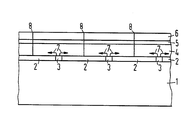
- the reference numeral 1 denotes a substrate body made of, for example, metallized glass or a flat silicon obtained by strip drawing. Then a highly doped, amorphous germanium layer 2 (a-Ge: P: H) with a phosphorus content of at least 1% by decomposing German (GeH.) And phosphine (PH,) in a low-pressure glow discharge reactor in a layer thickness of 0.2 deposited to 0.5 ⁇ m.
- a-Ge: P: H a highly doped, amorphous germanium layer 2 with a phosphorus content of at least 1% by decomposing German (GeH.) And phosphine (PH,) in a low-pressure glow discharge reactor in a layer thickness of 0.2 deposited to 0.5 ⁇ m.
- This germanium-phosphor layer 2 is crystallized with the aid of a pulsed or continuous wave laser of suitable wavelength (for germanium in the range of 1 ⁇ m) at certain points 3 (or lines), preferably with ⁇ 001> or ⁇ 111> orientation. This crystallization can also be achieved with an electron beam.
- ⁇ 001> and ⁇ 111> orientations are preferred crystal orientations for germanium.
- a subsequent gallium arsenide epitaxy carried out in a known manner and also suitable for the production of solar cells, for example from the organometallic compound Ga (CH,) and arsenic hydrogen or from arsenic hydrogen (AsH,) and gallium trichloride (GaCl 3 ) starts at the crystallization points (lines) 3.
- a deposition of gallium arsenide (4) on the amorphous areas of the germanium-phosphor layer 2 cannot take place due to the lack of lattice adaptation.
- the gallium arsenide of layer 4 starting from the predetermined crystallization points 3, the distances between which are preferably between 100 and 200 ⁇ m and the extent of which extends over approximately 5 ⁇ m, spreads laterally over the entire area in the direction of arrow 7 until the crystal fronts adjacent “epitaxial region” (3) meet.
- the growth areas are (001) or (111) areas.
- comm boundaries 8 are formed, which, however, are formed perpendicularly or approximately perpendicularly to the substrate surface 1 and thus have no appreciably harmful influence on the current collection of the solar cell.
- the grain boundaries 8 can be passivated by the hydrogen diffusing out of the amorphous germanium-phosphor layer 2 during epitaxy.
- the gallium arsenide is deposited at temperatures between 700 and 800 ° C, the gallium arsenide is deposited in crystalline form. At these temperatures, the amorphous germanium can crystallize, which favors gallium arsenide grain growth.
- the highly doped germanium-phosphor layer 2 forms the ohmic contact of the gallium arsenide solar cell with the conductive back contact (substrate 1).
- the crystallization structures (3) generated with the laser are selected in the range of 100 ⁇ m; this structure consequently also specifies the grain size. As is known from the literature, 10 ⁇ m grains are sufficient to achieve the high efficiency of monocrystalline gallium arsenide solar cells.
- a second gallium arsenide layer 5 of p-type with tin as dopant is deposited in a layer thickness of 0.2 to 1 ⁇ m in a known manner, and finally the arrangement is covered with a layer 6 consisting of a mixed aluminum-arsenic crystal.
- the layer 6, which has a layer thickness of 0.5 to .mu.m, is p-doped and serves as a window layer. It widens the band gap between the conduction and valence bands and prevents surface recombinations.
Abstract
Description
- Die Patentanmeldung betrifft ein Verfahren zum Herstellen von Dünnschicht-Solarzellen mit einem überwiegen aus Galliumarsenid bestehenden Halbleiterkörper, der durch epitaktische Abscheidung seiner Schichten aus der Gasphase auf einem elektrisch leitenden Substrat erzeugt wird und bei dem zur Begünstigung des epitaktischen Wachstums vor der Galliumarsenid-Abscheidung auf dem Substrat eine Germaniumschicht aufgebracht wird.
- Ein Veriahren dieser Art ist aus der DE-OS 2714243 zu entnehmen.
- Die Entwicklung von hocheffizienten (Wirkungsgrade größer 20 %), billigen und stabilen Solarzellen hat bis heute noch zu keinem zufriedenstellenden Ergebnis geführt. Es sind Dünnschicht-Solarzellen aus amorphem Silizium bekannt, die zwar kostengünstig im Glimmentladungsverfahren herstellbar sind, aber eine geringe Stabilität und einen zu niedrigen Wirkungsgrad (ungefähr 5 %) besitzen.
- Desweiteren sind kristalline Silizium-Solarzellen bekannt, die mit hoher Flächengeschwindigkeit in Bänder-oder Folienform kostengünstig hergestellt werden können, aber einen zu niedrigen Wirkungsgrad aufweisen.
- Ein hoher Wirkungsgrad wird erzielt, wenn die kristallinen Siliziumsolarzellen nach konventionellen Kristallzüchtungsverfahren, also mit niedriger Flächengeschwindig keil hergestellt werden. Sie sind relativ teuer und für eine Massenproduktion ungeeignet.
- Ein wichtiger Faktor bei der Herstellung kristalliner Solarzellen ist auch die Wahl geeigneten Ausgangsmaterials. Es soll billig und einfach verarbeitbar sein und die für einen hohen Wirkungsgrad entsprechende Reinheit besitzen.
- Dünnschicht-Solarzellen aus Galliumarsenid, wie beispielsweise aus der eingangs genannten DE-OS 2714243 bekannt, weisen einen höheren theoretischen Wirkungsgrad (24 bis 28 %) als die vorgenannten kristallinen Siliziumsolarzellen auf; die Herstellung der Galliumarsenid-Epitaxieschichten mit ausreichender Komgröße, vorzugsweise in Kolumnarstruktur, bereitet jedoch Schwierigkeiten. Ein weiteres Problem ist auch die Auswahl an billigem Substratmaterial mit Gitteranpassung.
- Die Erfindung stellt sich die Aufgabe, die eben beschriebenen Probleme zu lösen und auf der Basis von Galliumarsenid als Halbleiterkörper billige, hocheffiziente und stabile Solarzellen herzustellen.
- Die erfindungsgemäße Aufgabe wird bei einem Verfahren der eingangs genannten Art durch den Ablauf folgender Verfahrensschritte gelöst
-
- a) es werden billige Substrate wie metallisiertes Glas oder Flächensilizium verwendet, auf denen die Germaniumschicht hochdotiert und im amorphen Zustand niedergeschlagen wird,
- b) die amorphe Germaniumschicht wird an bestimmten vorgegebenen Punkten oder Linien mittels energiereicher Strahlung in Bezirke mit definierter Kristallorientierung übergeführt und
- c) die Parameter bei der Gasphasenepitaxie des GaJliumarsenid werden so eingestellt, daß sich ausgehend von den Kristallisationsbezirken die epitaktische Schicht lateral flächendeckend ausbreitet, bis die Kristallfront benachbarter Epitaxiebezirke aneinander stossen.
- Die Erfindung macht sich dabei die aus dem Aufsatz von Shirley S. Chu et al. aus dem Jorunal of Applied Physics, Vol. 48, Nr. 11, November 1977, auf den Seiten 4848 bis 4849 gewonnene Erkenntnis der Begünstigung des Wachstums von Galliumarsenidschichten auf rekristallisierten Germaniumschichten zunutze, verwendet aber zur Kristallisierung energiereiche Strahlung, wobei die erzeugten Kristallisationsstrukturen, die vorzugsweise im Bereich von 100 um liegen, die Korngröße in der wachsenden Schicht vorgeben.
- Vorteilhafte Weiterbildungen der Erfindung ergeben sich aus den Unteransprüchen.
- Die Erfindung wird im folgenden anhand der Figur, welche im Schnittbild eine durch das erfindungsgemäße Verfahren hergestellte Dünnschicht-Solarzelle darstellt, noch näher erläutert.
- Mit dem Bezugszeichen 1 ist ein Substratkörper aus beispielsweise metallisiertem Glas oder einem durch Bandziehen gewonnen Flächensilizium bezeichnet. Darauf wird eine hochdotierte, amorphe Germaniumschicht 2 (a-Ge:P:H) mit einem Phosphorgehalt von mindestens 1 % durch Zersetzen von German (GeH.) und Phosphin (PH,) in einem Niederdruck-Glimmentladungsreaktor in einer Schichtdicke von 0,2 bis 0,5 um abgeschieden.
- Diese Germanium-Phosphor-Schicht 2 wird mit Hilfe eines gepulsten oder Dauerstrich-Laser geeigneter Wellenlänge (für Germanium im Bereich von 1 um) an bestimmten Punk ten 3 (oder Linien) vorzugsweise mit < 001 > - oder < 111 > -Orientierung kristallisiert. Diese Kristallisierung läßt sich auch mit einem Elektronenstrahl erreichen. Die < 001 > - und die <111> -Orientierung sind bevorzugte Kristallorientierungen für Germanium.
- Eine nachfolgende, in bekannter Weise durchgeführte und auch für die Herstellung von Solarzellen geeignete Gallium-Arsenid-Epitaxie, zum Beispiel aus der metallorganischen Verbindung Ga(CH,), und Arsen-Wasserstoff oder aus Arsen-Wasserstoff (AsH,) und Galliumtrichlorid (GaCl3) setzt an den Kristallisationspunkten (Linien) 3 an. Eine Abscheidung von Galliumarsenid (4) auf den amorphen Bereichen der Germanium-Phosphor-Schicht 2 kann wegen der fehlenden Gitteranpassung nicht stattfinden.
- Das Gallium-Arsenid der Schicht 4 breitet sich ausgehend von den vorgegebenen Kristallisationspunkten 3, deren Abstände vorzugsweise zwischen 100 und 200 um liegen und deren Ausdehnung sich über ca. 5 um erstrecken, in Pfeilrichtung 7 lateral flächendeckend aus, bis die Kristallfronten benachbarter "Epitaxiebereich" (3) aufeinander treffen. Die Wachstumsflächen sind (001)- oder (111 )-Flächen. An den Treffpunkten bilden sich Komgrenzen 8, die sich aber senkrecht oder annähernd senkrecht zur Substratoberfläche 1 ausbilden und so für die Stromsammlung der Solarzelle keinen nennenswert schädlichen Einfluß ausüben. Außerdem können die Komgrenzen 8 durch den bei der Epitaxie aus der amorphen Germanium-Phosphor-Schicht 2 ausdiffundierenden Wasserstoff passiviert werden.
- Erfolgt die Abscheidung des Galliumarsenids bei Temperaturen zwischen 700 und 800°C, so scheidet sich das Galliumarsenid kristallin ab. Bei diesen Temperaturen kann das amorphe Germanium kristallisieren, wodurch das Galliumarsenid-Kornwachstum begünstigt wird. Die hoch dotierte Germanium-Phosphor-Schicht 2 bildet den ohmschen Kontakt der Galliumarsenid-Solarzelle zum leitenden Rückkontakt (Substrat 1).
- Die mit dem Laser erzeugten Kristallisationstrukturen (3) werden im Bereich von 100 um gewählt; diese Struktur gibt dann konsequenterweise auch die Korngröße vor. Wie aus der Literatur bekannt ist, reichen bereits 10 um große Körner aus, um den hohen Wirkungsgrad von monokristallinen Galliumarsenid-Solarzellen zu erreichen.
- Die erste Galliumarsenid-Schicht 4, welche beispielsweise mit einer aus Zink bestehenden Dotierung vom n-Leitungstyp abgeschieden wird, weist eine Schichtdicke von 3 bis 5 µm auf. Darauf wird in bekannter Weise eine zweite Galliumarsenid-Schicht 5 vom p-Leitungstyp mit Zinn als Dotierstoff in einer Schichtdicke von 0,2 bis 1 µm abgeschieden und schließlich die Anordnung mit einer Schicht 6 bestehend aus einem Galiium-Aluminium-Arsen-Mischkristall bedeckt. Die Schicht 6, welche eine Schichtdicke von 0,5 bis um aufweist, ist p-dotiert und dient als Fensterschicht. Sie weitet den Bandabstand zwischen Leitungs-und Valenzband auf und verhindert Oberflächenrekombinationen.
- Da die einzelnen Prozeßschritte nacheinander durch einfaches Zuschalten der verschiedenen Reaktionsgase in einem abgeschlossenen System ablaufen, wird in kostengünstiger Weise eine hohe Reinheit der amorphen hochdotierten Germaniumschicht 2 gewährleistet, so daß die sonst empfindliche Galliumarsenid-Gasphasenepitaxie von störenden Fremdkeimen nicht initiiert werden kann.
Claims (9)
Applications Claiming Priority (2)
| Application Number | Priority Date | Filing Date | Title |
|---|---|---|---|
| DE3437233 | 1984-10-10 | ||
| DE3437233 | 1984-10-10 |
Publications (2)
| Publication Number | Publication Date |
|---|---|
| EP0180751A2 true EP0180751A2 (de) | 1986-05-14 |
| EP0180751A3 EP0180751A3 (de) | 1988-09-07 |
Family
ID=6247604
Family Applications (1)
| Application Number | Title | Priority Date | Filing Date |
|---|---|---|---|
| EP85112052A Withdrawn EP0180751A3 (de) | 1984-10-10 | 1985-09-24 | Verfahren zum Herstellen von Galliumarsenid-Dünnschicht-Solar-zellen |
Country Status (3)
| Country | Link |
|---|---|
| US (1) | US4657603A (de) |
| EP (1) | EP0180751A3 (de) |
| JP (1) | JPS6195578A (de) |
Cited By (13)
| Publication number | Priority date | Publication date | Assignee | Title |
|---|---|---|---|---|
| EP0244081A1 (de) * | 1986-03-28 | 1987-11-04 | Canon Kabushiki Kaisha | Verfahren zur Herstellung eines Kristalls und Kristallkörper, die nach diesem Verfahren hergestellt werden |
| EP0276961A2 (de) * | 1987-01-26 | 1988-08-03 | Canon Kabushiki Kaisha | Sonnenzelle und ihr Herstellungsverfahren |
| EP0284434A2 (de) * | 1987-03-27 | 1988-09-28 | Canon Kabushiki Kaisha | Verfahren zur Herstellung von Kristallen |
| EP0284433A2 (de) * | 1987-03-27 | 1988-09-28 | Canon Kabushiki Kaisha | Kristalline Gegenstände und Verfahren zu ihrer Herstellung |
| EP0284441A2 (de) * | 1987-03-26 | 1988-09-28 | Canon Kabushiki Kaisha | Kristallisches Verbundprodukt der II-VI-Gruppe und Verfahren zu seiner Herstellung |
| EP0288166A2 (de) * | 1987-03-26 | 1988-10-26 | Canon Kabushiki Kaisha | Verfahren zur selektiven Herstellung von III-V Halbleiterschichten |
| EP0289117A2 (de) * | 1987-03-02 | 1988-11-02 | Canon Kabushiki Kaisha | Verfahren zur Herstellung von Kristallen auf einem Substrat |
| EP0334110A3 (en) * | 1988-03-24 | 1990-03-14 | Siemens Aktiengesellschaft | Process for producing polycristalline layers with large crystals for thin film semiconductor devices, like solar cells |
| US5010033A (en) * | 1987-03-27 | 1991-04-23 | Canon Kabushiki Kaisha | Process for producing compound semiconductor using an amorphous nucleation site |
| EP0484922A1 (de) * | 1990-11-07 | 1992-05-13 | Canon Kabushiki Kaisha | III-V Verbindungs-Halbleiter-Vorrichtung, Drucker- und Anzeigevorrichtung unter Verwendung derselben, und Verfahren zur Herstellung dieser Vorrichtung |
| US5254211A (en) * | 1987-03-27 | 1993-10-19 | Canon Kabushiki Kaisha | Method for forming crystals |
| DE19605245A1 (de) * | 1996-02-13 | 1997-08-14 | Siemens Ag | Verfahren zur Erzeugung von Kristallisationszentren auf der Oberfläche eines Substrats |
| US5846320A (en) * | 1986-03-31 | 1998-12-08 | Canon Kabushiki Kaisha | Method for forming crystal and crystal article obtained by said method |
Families Citing this family (31)
| Publication number | Priority date | Publication date | Assignee | Title |
|---|---|---|---|---|
| US4772564A (en) * | 1985-10-30 | 1988-09-20 | Astrosystems, Inc. | Fault tolerant thin-film photovoltaic cell fabrication process |
| US4781766A (en) * | 1985-10-30 | 1988-11-01 | Astrosystems, Inc. | Fault tolerant thin-film photovoltaic cell and method |
| JPS63108709A (ja) * | 1986-10-25 | 1988-05-13 | Toyota Central Res & Dev Lab Inc | 半導体装置およびその製造方法 |
| CA1331950C (en) * | 1987-03-26 | 1994-09-13 | Hiroyuki Tokunaga | Iii - v group compound crystal article and process for producing the same |
| US5281283A (en) * | 1987-03-26 | 1994-01-25 | Canon Kabushiki Kaisha | Group III-V compound crystal article using selective epitaxial growth |
| US5364815A (en) * | 1987-03-27 | 1994-11-15 | Canon Kabushiki Kaisha | Crystal articles and method for forming the same |
| US5304820A (en) * | 1987-03-27 | 1994-04-19 | Canon Kabushiki Kaisha | Process for producing compound semiconductor and semiconductor device using compound semiconductor obtained by same |
| EP0297867B1 (de) * | 1987-07-01 | 1993-10-06 | Nec Corporation | Verfahren zur Züchtung eines Halbleiterkristalles aus III-V-Gruppen-Verbindung auf einem Si-Substrat |
| US5363799A (en) * | 1987-08-08 | 1994-11-15 | Canon Kabushiki Kaisha | Method for growth of crystal |
| AU623601B2 (en) * | 1987-08-08 | 1992-05-21 | Canon Kabushiki Kaisha | Method for growth of crystal |
| AU623861B2 (en) * | 1987-08-08 | 1992-05-28 | Canon Kabushiki Kaisha | Crystal article, method for producing the same and semiconductor device utilizing the same |
| EP0307109A1 (de) * | 1987-08-24 | 1989-03-15 | Canon Kabushiki Kaisha | Verfahren zur Herstellung eines Halbleiterkristalls und dabei hergestellter Halbleiterkristall |
| EP0312202A1 (de) * | 1987-08-24 | 1989-04-19 | Canon Kabushiki Kaisha | Verfahren zur Herstellung eines Kristalls |
| US4914053A (en) * | 1987-09-08 | 1990-04-03 | Texas Instruments Incorporated | Heteroepitaxial selective-area growth through insulator windows |
| US4826784A (en) * | 1987-11-13 | 1989-05-02 | Kopin Corporation | Selective OMCVD growth of compound semiconductor materials on silicon substrates |
| JPH01315127A (ja) * | 1988-03-18 | 1989-12-20 | Fujitsu Ltd | ガリウムヒ素層の形成方法 |
| US5238879A (en) * | 1988-03-24 | 1993-08-24 | Siemens Aktiengesellschaft | Method for the production of polycrystalline layers having granular crystalline structure for thin-film semiconductor components such as solar cells |
| US4935385A (en) * | 1988-07-22 | 1990-06-19 | Xerox Corporation | Method of forming intermediate buffer films with low plastic deformation threshold using lattice mismatched heteroepitaxy |
| US4994867A (en) * | 1988-07-22 | 1991-02-19 | Xerox Corporation | Intermediate buffer films with low plastic deformation threshold for lattice mismatched heteroepitaxy |
| US5190613A (en) * | 1988-10-02 | 1993-03-02 | Canon Kabushiki Kaisha | Method for forming crystals |
| JP2858434B2 (ja) * | 1989-03-31 | 1999-02-17 | キヤノン株式会社 | 結晶の形成方法および結晶物品 |
| US5094697A (en) * | 1989-06-16 | 1992-03-10 | Canon Kabushiki Kaisha | Photovoltaic device and method for producing the same |
| US5256594A (en) * | 1989-06-16 | 1993-10-26 | Intel Corporation | Masking technique for depositing gallium arsenide on silicon |
| JPH076960A (ja) * | 1993-06-16 | 1995-01-10 | Fuji Electric Co Ltd | 多結晶半導体薄膜の生成方法 |
| JP3322440B2 (ja) * | 1993-06-24 | 2002-09-09 | 三洋電機株式会社 | 薄膜多結晶シリコンの製造方法 |
| US5897331A (en) * | 1996-11-08 | 1999-04-27 | Midwest Research Institute | High efficiency low cost thin film silicon solar cell design and method for making |
| US6184144B1 (en) | 1997-10-10 | 2001-02-06 | Cornell Research Foundation, Inc. | Methods for growing defect-free heteroepitaxial layers |
| ES2232299B1 (es) * | 2003-11-04 | 2006-03-16 | Isofoton, S.A. | Procedimientos de ensamblaje de modulos fotovoltaicos de concentracion. |
| DE102005045096A1 (de) * | 2005-09-21 | 2007-03-29 | Institut für Physikalische Hochtechnologie e.V. | Dünnschichtsolarzelle und Verfahren zur Herstellung eines Halbleiterbauelements |
| JP4921205B2 (ja) * | 2007-02-27 | 2012-04-25 | 株式会社えいむ | メニューブック |
| CN102479848A (zh) * | 2010-11-24 | 2012-05-30 | 吉富新能源科技(上海)有限公司 | 三五族半导体的太阳能电池结构及其制作方法 |
Family Cites Families (3)
| Publication number | Priority date | Publication date | Assignee | Title |
|---|---|---|---|---|
| US4053350A (en) * | 1975-07-11 | 1977-10-11 | Rca Corporation | Methods of defining regions of crystalline material of the group iii-v compounds |
| US4370510A (en) * | 1980-09-26 | 1983-01-25 | California Institute Of Technology | Gallium arsenide single crystal solar cell structure and method of making |
| US4392297A (en) * | 1980-11-20 | 1983-07-12 | Spire Corporation | Process of making thin film high efficiency solar cells |
-
1985
- 1985-09-20 US US06/778,487 patent/US4657603A/en not_active Expired - Fee Related
- 1985-09-24 EP EP85112052A patent/EP0180751A3/de not_active Withdrawn
- 1985-10-08 JP JP60222906A patent/JPS6195578A/ja active Pending
Non-Patent Citations (3)
| Title |
|---|
| APPLIED PHYSICS LETTERS, Band 41, Nr. 4, August 1982, Seiten 347-349, New York, US; B.-Y. TSAUR et al.: "Low-dislocation-density GaAs epilayers grown on Ge-coated Si substrates by means of lateral epitaxial overgrowth" * |
| EXTENDED ABSTRACTS, Band 84, Nr. 2, 1984, Seite 451, New Orleans, US; S.S. CHU et al.: "Gallium arsenide thin films on recrystallized germanium substrates" * |
| JOURNAL OF APPLIED PHYSICS, Band 48, Nr. 11, November 1977, Seiten 4848-4849, New York, US; S.S CHU et al.: "Gallium arsenide films on recrystallized germanium films" * |
Cited By (23)
| Publication number | Priority date | Publication date | Assignee | Title |
|---|---|---|---|---|
| US5733369A (en) * | 1986-03-28 | 1998-03-31 | Canon Kabushiki Kaisha | Method for forming crystal |
| US5853478A (en) * | 1986-03-28 | 1998-12-29 | Canon Kabushiki Kaisha | Method for forming crystal and crystal article obtained by said method |
| EP0244081A1 (de) * | 1986-03-28 | 1987-11-04 | Canon Kabushiki Kaisha | Verfahren zur Herstellung eines Kristalls und Kristallkörper, die nach diesem Verfahren hergestellt werden |
| EP0476713A3 (en) * | 1986-03-28 | 1992-08-05 | Canon Kabushiki Kaisha | Method for forming crystal and crystal article obtained by said method |
| US5846320A (en) * | 1986-03-31 | 1998-12-08 | Canon Kabushiki Kaisha | Method for forming crystal and crystal article obtained by said method |
| EP0276961A2 (de) * | 1987-01-26 | 1988-08-03 | Canon Kabushiki Kaisha | Sonnenzelle und ihr Herstellungsverfahren |
| EP0276961A3 (de) * | 1987-01-26 | 1989-03-08 | Canon Kabushiki Kaisha | Sonnenzelle und ihr Herstellungsverfahren |
| EP0289117A2 (de) * | 1987-03-02 | 1988-11-02 | Canon Kabushiki Kaisha | Verfahren zur Herstellung von Kristallen auf einem Substrat |
| EP0289117A3 (en) * | 1987-03-02 | 1989-03-15 | Canon Kabushiki Kaisha | Method of forming crystals on a substrate |
| EP0288166A2 (de) * | 1987-03-26 | 1988-10-26 | Canon Kabushiki Kaisha | Verfahren zur selektiven Herstellung von III-V Halbleiterschichten |
| EP0284441A2 (de) * | 1987-03-26 | 1988-09-28 | Canon Kabushiki Kaisha | Kristallisches Verbundprodukt der II-VI-Gruppe und Verfahren zu seiner Herstellung |
| EP0288166A3 (en) * | 1987-03-26 | 1989-10-04 | Canon Kabushiki Kaisha | Process for selective formation of iii - v group compound film |
| EP0284441A3 (de) * | 1987-03-26 | 1989-10-04 | Canon Kabushiki Kaisha | Kristallisches Verbundprodukt der II-VI-Gruppe und Verfahren zu seiner Herstellung |
| EP0284434A3 (de) * | 1987-03-27 | 1989-03-22 | Canon Kabushiki Kaisha | Verfahren zur Herstellung von Kristallen |
| US5010033A (en) * | 1987-03-27 | 1991-04-23 | Canon Kabushiki Kaisha | Process for producing compound semiconductor using an amorphous nucleation site |
| US5254211A (en) * | 1987-03-27 | 1993-10-19 | Canon Kabushiki Kaisha | Method for forming crystals |
| EP0284433A3 (de) * | 1987-03-27 | 1989-03-08 | Canon Kabushiki Kaisha | Kristalline Gegenstände und Verfahren zu ihrer Herstellung |
| EP0284433A2 (de) * | 1987-03-27 | 1988-09-28 | Canon Kabushiki Kaisha | Kristalline Gegenstände und Verfahren zu ihrer Herstellung |
| EP0284434A2 (de) * | 1987-03-27 | 1988-09-28 | Canon Kabushiki Kaisha | Verfahren zur Herstellung von Kristallen |
| EP0334110A3 (en) * | 1988-03-24 | 1990-03-14 | Siemens Aktiengesellschaft | Process for producing polycristalline layers with large crystals for thin film semiconductor devices, like solar cells |
| EP0484922A1 (de) * | 1990-11-07 | 1992-05-13 | Canon Kabushiki Kaisha | III-V Verbindungs-Halbleiter-Vorrichtung, Drucker- und Anzeigevorrichtung unter Verwendung derselben, und Verfahren zur Herstellung dieser Vorrichtung |
| US5659184A (en) * | 1990-11-07 | 1997-08-19 | Canon Kabushiki Kaisha | III-V compound semiconductor device with a polycrystalline structure with minimum grain size of 0.6 μm and printer and display device utilizing the same |
| DE19605245A1 (de) * | 1996-02-13 | 1997-08-14 | Siemens Ag | Verfahren zur Erzeugung von Kristallisationszentren auf der Oberfläche eines Substrats |
Also Published As
| Publication number | Publication date |
|---|---|
| US4657603A (en) | 1987-04-14 |
| EP0180751A3 (de) | 1988-09-07 |
| JPS6195578A (ja) | 1986-05-14 |
Similar Documents
| Publication | Publication Date | Title |
|---|---|---|
| EP0180751A2 (de) | Verfahren zum Herstellen von Galliumarsenid-Dünnschicht-Solar-zellen | |
| DE4019209C2 (de) | ||
| DE4019219C2 (de) | ||
| DE4138121C2 (de) | Verfahren zur Herstellung einer Solarzelle | |
| DE69530859T2 (de) | Verfahren zur herstellung einer mehrschicht-solarzelle | |
| DE3426338C2 (de) | ||
| DE2943211C2 (de) | Amorphe Halbleiter auf Silizium- und/oder Germaniumbasis, ihre Verwendung und ihre Herstellung durch Glimmentladung | |
| DE3823249A1 (de) | Halbleitereinrichtung | |
| DE2538325C2 (de) | Verfahren zur Herstellung von Halbleiterbauelementen | |
| DE3105819A1 (de) | Amorphe filmsolarzelle | |
| DE3119481A1 (de) | Verfahren zum herstellen einer p-leitfaehigen halbleiterlegierung | |
| DE3446956C2 (de) | ||
| DE2702860A1 (de) | Solarzelle und verfahren zu ihrer herstellung | |
| DE3244626A1 (de) | Sperrschicht-fotoelement und herstellungsverfahren dafuer | |
| DE2618733A1 (de) | Halbleiterbauelement mit heterouebergang | |
| DE2231926B2 (de) | Verfahren zur Herstellung von Halbleitermaterial | |
| DE2749607C3 (de) | Halbleiteranordnung und Verfahren zu deren Herstellung | |
| DE2844070A1 (de) | Amorpher halbleiter | |
| DE19634617A1 (de) | Solarzelle | |
| DE102012104140A1 (de) | Verbesserte Emitterstruktur und Verfahren zur Herstellung einer Silicium-Solarzelle mit Heteroübergang | |
| DE19622704A1 (de) | Epitaxialwafer und Verfahren zu seiner Herstellung | |
| DE2832153C2 (de) | Verfahren zur Herstellung von Halbleitervorrichtungen | |
| DE2154386B2 (de) | Verfahren zum Herstellen einer epitaktischen Halbleiterschicht auf einem Halbleitersubstrat durch Abscheiden aus einem Reaktionsgas/Trägergas-Gemisch | |
| WO2010057613A2 (de) | Tandemsolarzelle aus kristallinem silizium und kristallinem siliziumcarbid sowie verfahren zu dessen herstellung | |
| DE2752107A1 (de) | Elektrolumineszenzelement und verfahren zu seiner herstellung |
Legal Events
| Date | Code | Title | Description |
|---|---|---|---|
| PUAI | Public reference made under article 153(3) epc to a published international application that has entered the european phase |
Free format text: ORIGINAL CODE: 0009012 |
|
| AK | Designated contracting states |
Kind code of ref document: A2 Designated state(s): DE FR GB IT |
|
| PUAL | Search report despatched |
Free format text: ORIGINAL CODE: 0009013 |
|
| AK | Designated contracting states |
Kind code of ref document: A3 Designated state(s): DE FR GB IT |
|
| STAA | Information on the status of an ep patent application or granted ep patent |
Free format text: STATUS: THE APPLICATION IS DEEMED TO BE WITHDRAWN |
|
| 18D | Application deemed to be withdrawn |
Effective date: 19890331 |
|
| RIN1 | Information on inventor provided before grant (corrected) |
Inventor name: KRUEHLER, WOLFGANG, DR. Inventor name: GRABMAIER, JOSEF, DR. |