EP0170392B1 - High frequency connector - Google Patents
High frequency connector Download PDFInfo
- Publication number
- EP0170392B1 EP0170392B1 EP85304446A EP85304446A EP0170392B1 EP 0170392 B1 EP0170392 B1 EP 0170392B1 EP 85304446 A EP85304446 A EP 85304446A EP 85304446 A EP85304446 A EP 85304446A EP 0170392 B1 EP0170392 B1 EP 0170392B1
- Authority
- EP
- European Patent Office
- Prior art keywords
- connector
- conductor
- housing
- central conductor
- high frequency
- Prior art date
- Legal status (The legal status is an assumption and is not a legal conclusion. Google has not performed a legal analysis and makes no representation as to the accuracy of the status listed.)
- Expired - Lifetime
Links
Images


Classifications
-
- H—ELECTRICITY
- H01—ELECTRIC ELEMENTS
- H01R—ELECTRICALLY-CONDUCTIVE CONNECTIONS; STRUCTURAL ASSOCIATIONS OF A PLURALITY OF MUTUALLY-INSULATED ELECTRICAL CONNECTING ELEMENTS; COUPLING DEVICES; CURRENT COLLECTORS
- H01R24/00—Two-part coupling devices, or either of their cooperating parts, characterised by their overall structure
- H01R24/38—Two-part coupling devices, or either of their cooperating parts, characterised by their overall structure having concentrically or coaxially arranged contacts
- H01R24/40—Two-part coupling devices, or either of their cooperating parts, characterised by their overall structure having concentrically or coaxially arranged contacts specially adapted for high frequency
- H01R24/52—Two-part coupling devices, or either of their cooperating parts, characterised by their overall structure having concentrically or coaxially arranged contacts specially adapted for high frequency mounted in or to a panel or structure
-
- H—ELECTRICITY
- H01—ELECTRIC ELEMENTS
- H01R—ELECTRICALLY-CONDUCTIVE CONNECTIONS; STRUCTURAL ASSOCIATIONS OF A PLURALITY OF MUTUALLY-INSULATED ELECTRICAL CONNECTING ELEMENTS; COUPLING DEVICES; CURRENT COLLECTORS
- H01R2103/00—Two poles
Definitions
- a prior art connector 36 of the type using a glass bead 38 is shown.
- the bead 38 comprises a tube 39 made of metal and a center conductor pin 40 which is fixed in place by glass 42 at the center of the tube 38.
- the bead 38 is inserted into the housing 12 to align with a conductor on the microstrip substrate 14, then solder is poured into a bore 44 provided in the upper end of the housing 12 so as to fix the bead 38 in place, then the center conductor pin 40 and a conductor portion of the substrate 14 are soldered to each other, and then the connector 36 is screwed into the housing 12.
Description
- The present invention relates to a high frequency connector adapted for interconnecting a microstrip circuit and an external circuit and, more particularly, to a connector structure suited to connect transverse electromagnetic mode (TEM) waves which lie in a 0.3-30 GHz frequency band, and starts from DE-A-2603187.
- A microstrip substrate is an implementation recently developed for the circuit construction of various equipments of the kind which use the microwave band. One of the major problems with a microstrip substrate is the interconnection between the substrate and an external circuit. Figs. 1 and 2 show different prior art connectors which may be used to interconnect a conductor section of a microstrip substrate, which is received in a housing, to a coaxial cable. In Fig. 1, a
connector 10 is fit in abore 18 formed in awall 16 of ahousing 12, which accommodates amicrostrip substrate 14 therein. Specifically, theconnector 10 comprises ashell 20 provided with aflange 22 and amale screw 24 which is to mate with an external circuit, anintermediary insertion member 26 coupled in theshell 20 and in thebore 18 of thewall 16 of thehousing 12, and acenter conductor 28 supported by aninsulator 30 inside thehollow shell 20 andinsertion member 26. Before mounting theconnector 10 to thehousing 12, themicrostrip substrate 14 is fixed in a predetermined position inside thehousing 12. Then, theinsertion member 26 of theconnector 10 is inserted into thebore 18 of thehousing 12, then acenter conductor pin 34 provided with a connectingribbon 32 beforehand is inserted into a slittedportion 28a of thecenter conductor 28 from inside thehousing 12, and then theribbon 32 is soldered to a corresponding conductor portion on thesubstrate 14. - In Fig. 2, a
prior art connector 36 of the type using aglass bead 38 is shown. Thebead 38 comprises atube 39 made of metal and acenter conductor pin 40 which is fixed in place byglass 42 at the center of thetube 38. In assembly, thebead 38 is inserted into thehousing 12 to align with a conductor on themicrostrip substrate 14, then solder is poured into abore 44 provided in the upper end of thehousing 12 so as to fix thebead 38 in place, then thecenter conductor pin 40 and a conductor portion of thesubstrate 14 are soldered to each other, and then theconnector 36 is screwed into thehousing 12. - The problem with the connector configuration shown in Fig. 1 is that due to the substantial inductive impedance of the
ribbon 32 the voltage standing-wave ratio (VSWR) is high at frequencies higher than several gigaherzs. Another problem is that the connection of theribbon 32 requires extra steps. Meanwhile, the connector configuration shown in Fig. 2 is disadvantageous in that a considerable number of steps are necessary for thebead 38 to be fixed in place by solder, which is poured into thebore 44 of thehousing 12, and in that the manipulation for replacing the microstrip substrate is intricate. In addition, both the connectors shown in Figs. 1 and 2 are expensive to produce and need expensive structural parts. - In DE-A-2603187, there is described a coaxial connector having an inner conductor which projects from a body of insulating material. The body of insulating material is dimensioned to match an opening in the wall of the housing, so that with the help of the wall of the housing it is possible to guide the inner conductor into a position of contact with a conducting strip inside the housing in a mechanically stable manner.
- US-A-3601766 describes a member for terminating a coaxial cable, the members being screwed on to the end of the coaxial cable in such a way that the end of the inner conductor of the cable is deflected during screwing by a tapered head on the end of a centrally located conductor pin and held between an inner surface of an insulating insert and the tapered head in order to provide a good electrical contact between the inner conductor of the cable and conductor pin.
- The embodiments of the invention which are to be described below enable a microstrip circuit to be connected to an external circuit with a desired microwave transmission characteristic, using a connector which is simple in construction and easy to assemble.
- The scope of the invention is defined in claim 1.
- In one embodiment of the invention to be described there is a connector for interconnecting an external circuit with a high frequency circuit mounted on a housing. The connector includes a tubular shell made of metal for mounting on the housing, the tubular shell is hollow and functions as an external conductor, and an elongate central conductor extends on and along the central axis of the connector and is designed to connect at one end to the high frequency circuit and at the other end to the external circuit. A support member made of insulating material supports the central conductor in the tubular shell of the connector and the central conductor is cantilevered by the support member at a point of the central conductor which is remote from the one end. A tip of the one end is thus free and movable.
- The high frequency connector to be described has a portion of the central conductor which is designed to contact a high frequency microstrip circuit resiliently and is supported so that it can deviate from and return towards the central axis of the connector thereby promoting easy and positive interconnection. The connector is particularly, although not exclusively, applicable to TEM mode waves lying in the frequency band of 0.3-30 GHz.
- Prior art arrangements and embodiments of the invention will now be described, by way of example, with reference to the accompanying drawings in which:-
- Figs. 1 and 2 are sections each showing a prior art high frequency connector;
- Fig. 3 is a section of a high frequency connector embodying the present invention;
- Figs, 4 and 5 show the connector of Fig. 3 mounted on a housing, which has a microstrip substrate therein, as well as a mounting procedure;
- Fig. 6 is a section of a connector in accordance with another embodiment of the present invention;
- Fig. 7 shows the connector of Fig. 6 mounted on a housing, which has a microstrip substrate therein, as well as a mounting procedure;
- Fig. 8 is a section of a connector in accordance with another embodiment of the present invention;
- Fig. 9 shows the connector of Fig. 8 mounted on a housing, which has a microstrip substrate therein, as well as a mounting procedure;
- Figs. 10 and 11 are sections of a connector in accordance with another embodiment of the present invention which is positioned perpendicularly to a microstrip substrate;
- Fig. 12 is a perspective view of a portion of the microstrip substrate with which the tip of a center conductor of the connector shown in any of Figs. 3-11 makes contact;
- Fig. 13 is a plan view of the substrate portion of Fig. 12;
- Fig. 14 is a perspective view of a modification to the substrate portion shown in Fig. 12;
- Fig. 15 shows a manner of contact between a connector center conductor and a microstrip substrate conductor;
- Figs. 16A-16D show various configurations of that portion of a connector center condutor which makes contact with a microstrip substrate;
- Fig. 17 is a diagram explanatory of calculation associated with a cantilever which represents a connector center conductor;
- Fig. 18 is a perspective view of a pair of clamp jigs adapted to determine an amount deviation of a connector center conductor;
- Fig. 19 is a section of the clamp jig shown in Fig. 18; and
- Figs. 20A-20C are front views of different slit configurations which may be provided in a connector center conductor.
- While the high frequency connector of the present invention is susceptible of numerous physical embodiments, depending upon the environment and requirements of use, substantial numbers of the herein shown and described embodiments have been made, tested and used, and all have performed in an eminently satisfactory manner.
- Referring to Fig. 3, a connector embodying the present invention is shown and generally designated by the
reference numeral 50. Fig. 4 shows the connector of Fig. 3 in a position mounted on ahousing 66 which has a microstrip circuit therein. As shown, theconnector 50 comprises ashell 52 which includes amating member 54 which in turn is provided with amale screw 56 and aflange 58, and aninsulator 60 for supporting acenter conductor 62. The left end of thecenter conductor 62 as viewed in Fig. 3 is rigidly retained by theinsulator 60 inside themale screw 56. - A characteristic feature of the illustrative embodiment is that the
center conductor 62 is cantilevered at its side (right-hand side as viewed in Fig. 3) adapted to connect to a microstrip circuit and terminates at a free end at that side. In addition, thetip 62a of thecenter conductor 62 is deviated from the axis of theshell 52 and mechanically movable within a certain limited range. Theinsulator 60 is made of tetrafluoroethylene, or Teflon (trade name), or like low-loss dielectric material. Theinsulator 60 andcenter conductor 62 are prevented from rotating relative to theshell 52 byresin 64 which is injected and then cured. In Fig. 4, the lengthwise dimention of a projection included in themating member 54 coincides with the depth of abore 66a provided in thehousing 66 within the range of machining errors, so that the relative position between thecenter conductor 62 and themicrostrip substrate 68 is adequately restricted. Thecenter conductor 62 has aslit 62b at its left end as seen in the drawings in which a center conductor of another connector is engageable. - Two different methods are available for mounting the
connector 50 on thehousing 66. One of them is such that, as shown in Fig. 4, themicrostrip substrate 68 is fixed to thehousing 66, then theconnector 50 is inserted into thehousing 66 with thetip 62a of thecenter conductor 62 directed upwardly, and then theconnector 50 is rotated 180 degrees about its axis to cause theconductor tip 62a to abut against a conductor surface on themicrostrip substrate 68 under predetermined pressure. Preferably, athin sheet 70 of polyester or polyimid, for example, is placed between theconductor tip 62a and thesubstrate 68 in order to avoid possible damage to the conductor surface on thesubstrate 68. The other method is such that, as shown in Fig. 5, theconductor tip 62a is raised by means of awire 72 and then themicrostrip substrate 68 is inserted as indicated by an arrow to a predetermined fixing position. - The
conductor tip 62a may be formed using a shape-memorizing alloy. In such a case, theconnector 50 will be inserted into thehousing 66 after processing, such as cooling, thedeformable conductor tip 62a to a temperature other than room temperature to straighten it: upon return to room temperature, theconductor tip 62a will show a given amount of deviation to exert an adequate contact pressure on thesubstrate 68. - Referring to Figs. 6 and 7, another embodiment of the present invention is shown. A connector, generally 74, in accordance with this particular embodiment has the
mating member 54 of theshell 52 which is relatively short, thebore 66a in thehousing 66 being correspondingly reduced in depth. As shown in Fig. 7, theconnector 74 with such a configuration is held in an inclined position and then inserted into thebore 66a. Such eliminates the need for handling theconductor tip 62a in the manner shown in Fig. 5. - In any of the two embodiments described above, after the
connector housing 66, theflange 58 is fastened to thehousing 66 by means of screws or the like (not shown). - Referring to Fig. 8, another embodiment of the present invention is shown. A connector, generally 76, has the
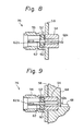
insulator 60 for supporting thecenter conductor 62 which is relatively short. Specifically, the dielectric which supports thecenter conductor 62 is dimensioned as small as possible so that thecenter conductor 62 may be surrounded by air, thereby increasing the cutoff frequency for needless modes. Theconnector 76 is shown in a mounted position in Fig. 9. - Referring to Figs. 10 and 11, another embodiment of the present invention is shown in which a
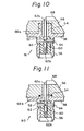
connector housing 66 such that thecenter conductor 62 extends perpendicular to themicrostrip substrate 68. In Fig. 10, theshell 52 is provided with a relativelylong mating member 54 while, in Fig. 11, it is provided with a relativelyshort mating member 54. In any of the configurations shown in Figs. 10 and 11, as shown in Fig. 12, a generally L-shaped conductor piece, or contact, 84 is thermally bonded or soldered to an end of aconductor 82 which is provided on the surface of themicrostrip substrate 68. This particular portion of thesubstrate 68 is shown in a plan view in Fig. 13. Alternatively, as shown in Fig. 14, aside conductor 86 may be provided on thesubstrate 68 by baking a conductor paste. - As shown in Fig. 15, the
conductor tip 62a having a circular cross-section makes line-to-line contact with theconductor 82 on thesubstrate 68. Conductors having a circular cross-section are inexpensive to produce and, therefore, suitably applicable to general-purpose high frequency connectors. However, concerning millimeter wave applications, contacting portions of the center conductors should preferably be machined in order to allow a minimum of discontinuity of the line. Preferred configurations of the contacting portions of a center conductor are shown in sections in Figs. 16A-16D. In Fig. 16A, aflat surface 88 which extends in one direction is included in the contact surface of the center conductor. In Fig. 16B,flat surfaces 90 extend in three different directions each conforming to the width of a conductor on thesubstrate 68. In Fig. 16C, alug 92 having a rectangular section protrudes from the center conductor; this configuration is desirably applicable to the embodiment of Figs. 10 and 11 in which thecenter conductor 62 and thesubstrate 68 are perpendicular to each other. To further enhance the contact, thelug 92 shown in Fig. 16C may be provided with arecess 94 in a lower part thereof, as shown in Fig. 16D. - As described above, the connector in accordance with any of the foregoing embodiments is capable of holding the
center conductor 62 in contact with the conductor surface on themicrostrip substrate 68 under adequate pressure. While the contact pressure in terms of normal component of a force of the contact surface is generally regarded acceptable if on the order of 0.2 N (Newton) in the case of gold (Au)-to-gold contact, it should preferably be about 5-12 N taking into account possible silver (Ag)-to-silver contact and entry of impurities between the contact surfaces. The magnitude of the normal component of a force on the contact surface will be described with reference to Fig. 17. - Referring to Fig. 17, assume that the
center conductor 62 has a length I in a cantilevered position, and that the free end of the length I is at a coordinate x = 0. A perpendicular load W acting on the free end causes the cantilever to deform in a direction y by an amount which is expressed as

center conductor 62 which is equal to or greater than 5 which is produced by the above equation. In practice, the deviation 0 of thecenter conductor 62 is preferably accomplished by holding thecenter conductor 62 beween a pair of clamp jigs 96 and 98 as shown in Fig. 18 and applying heat thereto. Thejigs center conductor 62 held therebetween. The deviation 5 is variable with the thickness of aspacer 100. - The
slit 62a provided in the center conductor adjacent to an external circuit may have any suitable configuration such as shown in Figs. 20A-20B. - In summary, it will be seen that the present invention provides a high frequency connector which achieves various advantages as enumerated below:
- (1) A microstrip circuit and a center conductor of a connector are directly connected to eliminate the need for an extra part otherwise required for the interconnection;
- (2) Therefore, the interconnection is set up by a minimum number of steps;
- (3) The interconnection is significantly stable partly because the circuit and the center conductor are constantly held in contact under predetermined pressure and partly because the center conductor absorbs any small error possibly developing in the distance between the circuit and the connector;
- (4) The interconnection work is simple and does not require any skill;
- (5) Since the contact pressure between the circuit and the center conductor is constant, the circuit is prevented from being damaged at the point of interconnection;
- (6) No part is mounted on the center conductor to simplify interconnection of the center conductor to the circuit and, thereby, enhance machining precision as well as precision of the assembly, so that an excellent high frequency transmission characteristic is attained; and
- (7) The connector is inexpensive to produce because it can be mechanically produced on a quantity basis, does not need any additional part for interconnection, and remarkably reduces the steps involved in the interconnection.
Claims (4)
Applications Claiming Priority (3)
| Application Number | Priority Date | Filing Date | Title |
|---|---|---|---|
| JP59132618A JPS6113583A (en) | 1984-06-27 | 1984-06-27 | High frequency connector |
| JP132618/84 | 1984-06-27 | ||
| JP13261884 | 1984-06-27 |
Publications (4)
| Publication Number | Publication Date |
|---|---|
| EP0170392A2 EP0170392A2 (en) | 1986-02-05 |
| EP0170392A3 EP0170392A3 (en) | 1987-08-26 |
| EP0170392B1 true EP0170392B1 (en) | 1991-10-30 |
| EP0170392B2 EP0170392B2 (en) | 2000-06-28 |
Family
ID=15085540
Family Applications (1)
| Application Number | Title | Priority Date | Filing Date |
|---|---|---|---|
| EP85304446A Expired - Lifetime EP0170392B2 (en) | 1984-06-27 | 1985-06-21 | High frequency connector |
Country Status (5)
| Country | Link |
|---|---|
| US (1) | US4669805A (en) |
| EP (1) | EP0170392B2 (en) |
| JP (1) | JPS6113583A (en) |
| CA (1) | CA1249350A (en) |
| DE (1) | DE3584548D1 (en) |
Families Citing this family (49)
| Publication number | Priority date | Publication date | Assignee | Title |
|---|---|---|---|---|
| EP0259163A3 (en) * | 1986-09-05 | 1989-07-12 | Tektronix, Inc. | Semiconductor wafer probe |
| JPS63291374A (en) * | 1987-05-22 | 1988-11-29 | Junkosha Co Ltd | Connector |
| DE3811752A1 (en) * | 1988-04-08 | 1989-10-19 | Rohde & Schwarz | Miniature HF coaxial jack |
| SE461429B (en) * | 1988-06-16 | 1990-02-12 | Ericsson Telefon Ab L M | CONNECTOR TO A MICROWAVE DEVICE |
| US4855697A (en) * | 1988-06-27 | 1989-08-08 | Cascade Microtech, Inc. | Coaxial transmission line to microstrip transmission line launcher |
| US4975065A (en) * | 1989-09-26 | 1990-12-04 | Avantek, Inc. | Microwave circuit module connector |
| US5416453A (en) * | 1989-09-29 | 1995-05-16 | Hughes Aircraft Company | Coaxial-to-microstrip orthogonal launchers having troughline convertors |
| EP0539956A1 (en) * | 1991-10-31 | 1993-05-05 | Hughes Aircraft Company | Coaxial to microstrip transition |
| FR2687852A1 (en) * | 1992-02-26 | 1993-08-27 | Dassault Electronique | CONNECTION DEVICE BETWEEN AN ANTENNA AND A MICROELECTRONIC HOUSING. |
| US5402088A (en) * | 1992-12-03 | 1995-03-28 | Ail Systems, Inc. | Apparatus for the interconnection of radio frequency (RF) monolithic microwave integrated circuits |
| US5356298A (en) * | 1993-04-01 | 1994-10-18 | Trw Inc. | Wideband solderless right-angle RF interconnect |
| US5618205A (en) * | 1993-04-01 | 1997-04-08 | Trw Inc. | Wideband solderless right-angle RF interconnect |
| FR2704361B1 (en) * | 1993-04-21 | 1995-07-13 | Philips Electronics Nv | HIGH FREQUENCY CONNECTION DEVICE. |
| US5683255A (en) * | 1993-12-03 | 1997-11-04 | Menze; Marion John | Radio frequency connector assembly |
| US5563562A (en) * | 1995-03-24 | 1996-10-08 | Itt Industries, Inc. | RF feed-through connector |
| US6091971A (en) * | 1997-08-18 | 2000-07-18 | Lucent Technologies Inc. | Plumbing wireless phones and apparatus thereof |
| US5971770A (en) * | 1997-11-05 | 1999-10-26 | Labinal Components And Systems, Inc. | Coaxial connector with bellows spring portion or raised bump |
| US6323743B1 (en) | 1999-08-24 | 2001-11-27 | Tresness Irrevocable Patent Trust | Electronic filter assembly |
| US6547593B1 (en) | 2000-08-07 | 2003-04-15 | Gore Enterprise Holdings, Inc. | Sub-miniature, high speed coaxial pin interconnection system |
| US6273766B1 (en) * | 2000-09-08 | 2001-08-14 | Eagle Comtronics, Inc. | Electronic device including a collet assembly with dual receiving sockets |
| DE20114544U1 (en) | 2000-12-04 | 2002-02-21 | Cascade Microtech Inc | wafer probe |
| US6692267B1 (en) * | 2001-08-23 | 2004-02-17 | Ciena Corporation | Printed circuit board testing module |
| AU2003233659A1 (en) | 2002-05-23 | 2003-12-12 | Cascade Microtech, Inc. | Probe for testing a device under test |
| US6663424B1 (en) * | 2002-05-30 | 2003-12-16 | Rockwell Collins, Inc. | Ultra wideband interconnect solution |
| US6724205B1 (en) | 2002-11-13 | 2004-04-20 | Cascade Microtech, Inc. | Probe for combined signals |
| US6870448B2 (en) * | 2003-03-14 | 2005-03-22 | Agilent Technologies, Inc. | Adjustable coaxial support |
| US6765461B1 (en) | 2003-04-30 | 2004-07-20 | Agilent Technologies, Inc. | Asymmetric support for high frequency transmission lines |
| US7057404B2 (en) | 2003-05-23 | 2006-06-06 | Sharp Laboratories Of America, Inc. | Shielded probe for testing a device under test |
| US6816039B1 (en) | 2003-07-10 | 2004-11-09 | Agilent Technologies, Inc. | Coaxial split-bead glass-to-metal seal for high frequency transmission line |
| WO2005065258A2 (en) | 2003-12-24 | 2005-07-21 | Cascade Microtech, Inc. | Active wafer probe |
| US7168979B2 (en) * | 2004-08-05 | 2007-01-30 | Agilent Technologies, Inc. | Microwave connector |
| JP2008512680A (en) | 2004-09-13 | 2008-04-24 | カスケード マイクロテック インコーポレイテッド | Double-sided probing structure |
| US7656172B2 (en) | 2005-01-31 | 2010-02-02 | Cascade Microtech, Inc. | System for testing semiconductors |
| US7535247B2 (en) | 2005-01-31 | 2009-05-19 | Cascade Microtech, Inc. | Interface for testing semiconductors |
| US7403028B2 (en) | 2006-06-12 | 2008-07-22 | Cascade Microtech, Inc. | Test structure and probe for differential signals |
| US7764072B2 (en) | 2006-06-12 | 2010-07-27 | Cascade Microtech, Inc. | Differential signal probing system |
| US7723999B2 (en) | 2006-06-12 | 2010-05-25 | Cascade Microtech, Inc. | Calibration structures for differential signal probing |
| US7876114B2 (en) | 2007-08-08 | 2011-01-25 | Cascade Microtech, Inc. | Differential waveguide probe |
| US7575474B1 (en) | 2008-06-10 | 2009-08-18 | Harris Corporation | Surface mount right angle connector including strain relief and associated methods |
| TWI446664B (en) * | 2010-05-18 | 2014-07-21 | Hon Hai Prec Ind Co Ltd | Cable connector assembly |
| US8480409B2 (en) * | 2010-12-13 | 2013-07-09 | Raytheon Company | Method for RF connector grounding |
| US20120264072A1 (en) * | 2011-02-03 | 2012-10-18 | Stion Corporation | Method and apparatus for performing reactive thermal treatment of thin film pv material |
| CN102751633B (en) * | 2012-07-18 | 2014-10-01 | 上海航天科工电器研究院有限公司 | Radio-frequency adaptor of floating structure |
| CN102977250B (en) * | 2012-12-30 | 2016-03-30 | 南京肯特复合材料有限公司 | Modified Teflon, manufacture method and the application on high frequency connectors thereof |
| EP2876747B1 (en) | 2013-11-21 | 2018-04-25 | Spinner GmbH | RF connector assembly |
| EP3432424A1 (en) | 2017-07-20 | 2019-01-23 | Spinner GmbH | Rf connector with a surface-mount interface |
| WO2019074470A1 (en) * | 2017-10-09 | 2019-04-18 | Keysight Technologies, Inc. | Hybrid coaxial cable fabrication |
| RU188349U1 (en) * | 2018-12-20 | 2019-04-09 | Российская Федерация, От Имени Которой Выступает Министерство Промышленности И Торговли Российской Федерации | SUPERWIDEBAND TRANSITION |
| EP3996201A4 (en) * | 2019-07-03 | 2023-07-19 | Kabushiki Kaisha Toshiba | Coaxial microstrip line conversion circuit |
Family Cites Families (21)
| Publication number | Priority date | Publication date | Assignee | Title |
|---|---|---|---|---|
| US3111352A (en) * | 1959-11-16 | 1963-11-19 | Ibm | Superconductive solderless connector |
| US3239713A (en) * | 1963-03-25 | 1966-03-08 | Microwave Ass | High frequency mode transformation between balanced transmission line and waveguide, useful in travelling wave tubes |
| US3242456A (en) * | 1963-10-07 | 1966-03-22 | Itt | Electrical connector with spring pin contact |
| US3601766A (en) * | 1969-02-13 | 1971-08-24 | Vernon F Alibert | Connector device for supporting cables and for additionally providing an electrical connection |
| US3622915A (en) * | 1970-03-16 | 1971-11-23 | Meca Electronics Inc | Electrical coupler |
| US3705379A (en) * | 1971-05-14 | 1972-12-05 | Amp Inc | Connector for interconnection of symmetrical and asymmetrical transmission lines |
| US3783321A (en) * | 1972-03-23 | 1974-01-01 | Adams Russel Co Inc | Coaxial connector |
| JPS5149497B2 (en) * | 1972-08-14 | 1976-12-27 | ||
| JPS5141696B2 (en) * | 1973-04-03 | 1976-11-11 | ||
| JPS5149497U (en) * | 1974-10-11 | 1976-04-14 | ||
| US3975077A (en) * | 1975-05-12 | 1976-08-17 | Honeywell Inc. | Electrical connector |
| JPS5141696U (en) * | 1975-09-11 | 1976-03-27 | ||
| DE2603187C3 (en) * | 1976-01-28 | 1980-01-10 | Siemens Ag, 1000 Berlin Und 8000 Muenchen | Coaxial connector |
| JPS5353897U (en) * | 1976-10-09 | 1978-05-09 | ||
| US4159505A (en) * | 1977-06-16 | 1979-06-26 | The Bendix Corporation | Packaging assembly for electronic mechanism |
| JPS5422955U (en) * | 1977-07-14 | 1979-02-15 | ||
| JPS54147697U (en) * | 1978-04-07 | 1979-10-13 | ||
| US4280112A (en) * | 1979-02-21 | 1981-07-21 | Eisenhart Robert L | Electrical coupler |
| FR2483131A1 (en) * | 1980-05-23 | 1981-11-27 | Radiall Sa | COAXIAL CONNECTOR ELEMENT |
| US4487465A (en) * | 1981-12-07 | 1984-12-11 | Raychem Corporation | Heat recoverable connecting device |
| US4516815A (en) * | 1982-06-07 | 1985-05-14 | Spectrum Control, Inc. | RF filter connector |
-
1984
- 1984-06-27 JP JP59132618A patent/JPS6113583A/en active Granted
-
1985
- 1985-06-21 EP EP85304446A patent/EP0170392B2/en not_active Expired - Lifetime
- 1985-06-21 DE DE8585304446T patent/DE3584548D1/en not_active Expired - Fee Related
- 1985-06-21 US US06/747,658 patent/US4669805A/en not_active Expired - Lifetime
- 1985-06-21 CA CA000484721A patent/CA1249350A/en not_active Expired
Also Published As
| Publication number | Publication date |
|---|---|
| EP0170392A2 (en) | 1986-02-05 |
| JPS6113583A (en) | 1986-01-21 |
| US4669805A (en) | 1987-06-02 |
| CA1249350A (en) | 1989-01-24 |
| EP0170392A3 (en) | 1987-08-26 |
| JPH0312433B2 (en) | 1991-02-20 |
| EP0170392B2 (en) | 2000-06-28 |
| DE3584548D1 (en) | 1991-12-05 |
Similar Documents
| Publication | Publication Date | Title |
|---|---|---|
| EP0170392B1 (en) | High frequency connector | |
| US5570068A (en) | Coaxial-to-coplanar-waveguide transmission line connector using integrated slabline transition | |
| US4957456A (en) | Self-aligning RF push-on connector | |
| USRE37368E1 (en) | High density, high bandwidth, coaxial cable, flexible circuit and circuit board connection assembly | |
| US4463324A (en) | Miniature coaxial line to waveguide transition | |
| EP0211949B1 (en) | Coaxial cable terminator | |
| KR20050054912A (en) | Electrical contact | |
| KR20040024591A (en) | Self-adjusted subminiature coaxial connector | |
| EP0362841B1 (en) | Controlled impedance plug and receptacle | |
| US4686498A (en) | Coaxial connector | |
| US20020016096A1 (en) | Method for assembling a circuit board apparatus with pin connectors | |
| EP0415601B1 (en) | Precision test connector | |
| US4666230A (en) | Coaxial cable connector assembly | |
| US20220271482A1 (en) | Rf connector | |
| US4291936A (en) | Coaxial connector with improved female conductor structure | |
| JP2002373743A (en) | Coaxial connector | |
| JPS63294674A (en) | Electric cable connector and its application | |
| CN1126211C (en) | Electrical receptacle | |
| CN219321683U (en) | Adjustable armored cable assembly | |
| US7049903B2 (en) | Transition from a coaxial transmission line to a printed circuit transmission line | |
| KR100880713B1 (en) | Right angle coaxial connector mountable on pcb | |
| JP2537567Y2 (en) | connector | |
| CN116053835A (en) | Adjustable armored cable assembly and assembling method thereof | |
| JP3432732B2 (en) | Structure of L-shaped coaxial connector connection part of electronic equipment | |
| JPH0421313B2 (en) |
Legal Events
| Date | Code | Title | Description |
|---|---|---|---|
| PUAI | Public reference made under article 153(3) epc to a published international application that has entered the european phase |
Free format text: ORIGINAL CODE: 0009012 |
|
| 17P | Request for examination filed |
Effective date: 19850702 |
|
| AK | Designated contracting states |
Designated state(s): DE FR GB |
|
| PUAL | Search report despatched |
Free format text: ORIGINAL CODE: 0009013 |
|
| AK | Designated contracting states |
Kind code of ref document: A3 Designated state(s): DE FR GB |
|
| RHK1 | Main classification (correction) |
Ipc: H01R 23/68 |
|
| 17Q | First examination report despatched |
Effective date: 19890629 |
|
| GRAA | (expected) grant |
Free format text: ORIGINAL CODE: 0009210 |
|
| AK | Designated contracting states |
Kind code of ref document: B1 Designated state(s): DE FR GB |
|
| REF | Corresponds to: |
Ref document number: 3584548 Country of ref document: DE Date of ref document: 19911205 |
|
| ET | Fr: translation filed | ||
| PLBI | Opposition filed |
Free format text: ORIGINAL CODE: 0009260 |
|
| 26 | Opposition filed |
Opponent name: ANT NACHRICHTENTECHNIK GMBH Effective date: 19920523 |
|
| PLAB | Opposition data, opponent's data or that of the opponent's representative modified |
Free format text: ORIGINAL CODE: 0009299OPPO |
|
| R26 | Opposition filed (corrected) |
Opponent name: BOSCH TELECOM GMBH Effective date: 19920523 |
|
| PLAW | Interlocutory decision in opposition |
Free format text: ORIGINAL CODE: EPIDOS IDOP |
|
| PLAW | Interlocutory decision in opposition |
Free format text: ORIGINAL CODE: EPIDOS IDOP |
|
| PUAH | Patent maintained in amended form |
Free format text: ORIGINAL CODE: 0009272 |
|
| STAA | Information on the status of an ep patent application or granted ep patent |
Free format text: STATUS: PATENT MAINTAINED AS AMENDED |
|
| 27A | Patent maintained in amended form |
Effective date: 20000628 |
|
| AK | Designated contracting states |
Kind code of ref document: B2 Designated state(s): DE FR GB |
|
| RIC2 | Information provided on ipc code assigned after grant |
Free format text: 7H 01R 12/16 A, 7H 01R 13/646 B |
|
| ET3 | Fr: translation filed ** decision concerning opposition | ||
| REG | Reference to a national code |
Ref country code: GB Ref legal event code: IF02 |
|
| PGFP | Annual fee paid to national office [announced via postgrant information from national office to epo] |
Ref country code: FR Payment date: 20030610 Year of fee payment: 19 |
|
| PGFP | Annual fee paid to national office [announced via postgrant information from national office to epo] |
Ref country code: GB Payment date: 20030618 Year of fee payment: 19 |
|
| PGFP | Annual fee paid to national office [announced via postgrant information from national office to epo] |
Ref country code: DE Payment date: 20030707 Year of fee payment: 19 |
|
| PG25 | Lapsed in a contracting state [announced via postgrant information from national office to epo] |
Ref country code: GB Free format text: LAPSE BECAUSE OF NON-PAYMENT OF DUE FEES Effective date: 20040621 |
|
| PG25 | Lapsed in a contracting state [announced via postgrant information from national office to epo] |
Ref country code: DE Free format text: LAPSE BECAUSE OF NON-PAYMENT OF DUE FEES Effective date: 20050101 |
|
| GBPC | Gb: european patent ceased through non-payment of renewal fee |
Effective date: 20040621 |
|
| PG25 | Lapsed in a contracting state [announced via postgrant information from national office to epo] |
Ref country code: FR Free format text: LAPSE BECAUSE OF NON-PAYMENT OF DUE FEES Effective date: 20050228 |
|
| REG | Reference to a national code |
Ref country code: FR Ref legal event code: ST |