EP0169326B1 - Verfahren und Vorrichtung zur Erzeugung eines makroskopischen Flächenmusters mit einer mikroskopischen Struktur, insbesondere einer beugungsoptisch wirksamen Struktur - Google Patents
Verfahren und Vorrichtung zur Erzeugung eines makroskopischen Flächenmusters mit einer mikroskopischen Struktur, insbesondere einer beugungsoptisch wirksamen Struktur Download PDFInfo
- Publication number
- EP0169326B1 EP0169326B1 EP85106087A EP85106087A EP0169326B1 EP 0169326 B1 EP0169326 B1 EP 0169326B1 EP 85106087 A EP85106087 A EP 85106087A EP 85106087 A EP85106087 A EP 85106087A EP 0169326 B1 EP0169326 B1 EP 0169326B1
- Authority
- EP
- European Patent Office
- Prior art keywords
- embossing
- thermoplastic layer
- focal spot
- embossing die
- punch
- Prior art date
- Legal status (The legal status is an assumption and is not a legal conclusion. Google has not performed a legal analysis and makes no representation as to the accuracy of the status listed.)
- Expired
Links
- 238000000034 method Methods 0.000 title claims abstract description 26
- 238000004049 embossing Methods 0.000 claims abstract description 67
- 229920001169 thermoplastic Polymers 0.000 claims abstract description 32
- 239000004416 thermosoftening plastic Substances 0.000 claims abstract description 32
- 239000000758 substrate Substances 0.000 claims description 11
- 238000006073 displacement reaction Methods 0.000 claims description 5
- 238000002310 reflectometry Methods 0.000 claims description 5
- 230000000694 effects Effects 0.000 claims description 4
- 230000005693 optoelectronics Effects 0.000 claims description 3
- 230000001360 synchronised effect Effects 0.000 claims 2
- 238000004519 manufacturing process Methods 0.000 claims 1
- 230000003287 optical effect Effects 0.000 abstract description 7
- 239000012815 thermoplastic material Substances 0.000 abstract 1
- 230000005855 radiation Effects 0.000 description 5
- 239000011324 bead Substances 0.000 description 2
- 230000015572 biosynthetic process Effects 0.000 description 2
- 230000001427 coherent effect Effects 0.000 description 2
- 238000001816 cooling Methods 0.000 description 2
- 238000010586 diagram Methods 0.000 description 2
- 238000000465 moulding Methods 0.000 description 2
- 230000000717 retained effect Effects 0.000 description 2
- 238000003786 synthesis reaction Methods 0.000 description 2
- OKTJSMMVPCPJKN-UHFFFAOYSA-N Carbon Chemical compound [C] OKTJSMMVPCPJKN-UHFFFAOYSA-N 0.000 description 1
- 229910000990 Ni alloy Inorganic materials 0.000 description 1
- 239000011358 absorbing material Substances 0.000 description 1
- 238000010521 absorption reaction Methods 0.000 description 1
- 230000004913 activation Effects 0.000 description 1
- 229910052799 carbon Inorganic materials 0.000 description 1
- 238000004040 coloring Methods 0.000 description 1
- 238000012217 deletion Methods 0.000 description 1
- 230000037430 deletion Effects 0.000 description 1
- 238000011161 development Methods 0.000 description 1
- 230000018109 developmental process Effects 0.000 description 1
- 238000010438 heat treatment Methods 0.000 description 1
- 239000002184 metal Substances 0.000 description 1
- 229910052751 metal Inorganic materials 0.000 description 1
- 239000004033 plastic Substances 0.000 description 1
- 239000002985 plastic film Substances 0.000 description 1
- 229920006255 plastic film Polymers 0.000 description 1
- 238000003825 pressing Methods 0.000 description 1
- 238000005096 rolling process Methods 0.000 description 1
- 239000000126 substance Substances 0.000 description 1
Images
Classifications
-
- G—PHYSICS
- G03—PHOTOGRAPHY; CINEMATOGRAPHY; ANALOGOUS TECHNIQUES USING WAVES OTHER THAN OPTICAL WAVES; ELECTROGRAPHY; HOLOGRAPHY
- G03H—HOLOGRAPHIC PROCESSES OR APPARATUS
- G03H1/00—Holographic processes or apparatus using light, infrared or ultraviolet waves for obtaining holograms or for obtaining an image from them; Details peculiar thereto
- G03H1/02—Details of features involved during the holographic process; Replication of holograms without interference recording
- G03H1/0276—Replicating a master hologram without interference recording
- G03H1/028—Replicating a master hologram without interference recording by embossing
-
- B—PERFORMING OPERATIONS; TRANSPORTING
- B29—WORKING OF PLASTICS; WORKING OF SUBSTANCES IN A PLASTIC STATE IN GENERAL
- B29C—SHAPING OR JOINING OF PLASTICS; SHAPING OF MATERIAL IN A PLASTIC STATE, NOT OTHERWISE PROVIDED FOR; AFTER-TREATMENT OF THE SHAPED PRODUCTS, e.g. REPAIRING
- B29C59/00—Surface shaping of articles, e.g. embossing; Apparatus therefor
- B29C59/02—Surface shaping of articles, e.g. embossing; Apparatus therefor by mechanical means, e.g. pressing
-
- G—PHYSICS
- G06—COMPUTING; CALCULATING OR COUNTING
- G06K—GRAPHICAL DATA READING; PRESENTATION OF DATA; RECORD CARRIERS; HANDLING RECORD CARRIERS
- G06K1/00—Methods or arrangements for marking the record carrier in digital fashion
- G06K1/12—Methods or arrangements for marking the record carrier in digital fashion otherwise than by punching
- G06K1/126—Methods or arrangements for marking the record carrier in digital fashion otherwise than by punching by photographic or thermographic registration
-
- G—PHYSICS
- G06—COMPUTING; CALCULATING OR COUNTING
- G06K—GRAPHICAL DATA READING; PRESENTATION OF DATA; RECORD CARRIERS; HANDLING RECORD CARRIERS
- G06K19/00—Record carriers for use with machines and with at least a part designed to carry digital markings
- G06K19/06—Record carriers for use with machines and with at least a part designed to carry digital markings characterised by the kind of the digital marking, e.g. shape, nature, code
- G06K19/08—Record carriers for use with machines and with at least a part designed to carry digital markings characterised by the kind of the digital marking, e.g. shape, nature, code using markings of different kinds or more than one marking of the same kind in the same record carrier, e.g. one marking being sensed by optical and the other by magnetic means
- G06K19/10—Record carriers for use with machines and with at least a part designed to carry digital markings characterised by the kind of the digital marking, e.g. shape, nature, code using markings of different kinds or more than one marking of the same kind in the same record carrier, e.g. one marking being sensed by optical and the other by magnetic means at least one kind of marking being used for authentication, e.g. of credit or identity cards
- G06K19/16—Record carriers for use with machines and with at least a part designed to carry digital markings characterised by the kind of the digital marking, e.g. shape, nature, code using markings of different kinds or more than one marking of the same kind in the same record carrier, e.g. one marking being sensed by optical and the other by magnetic means at least one kind of marking being used for authentication, e.g. of credit or identity cards the marking being a hologram or diffraction grating
-
- B—PERFORMING OPERATIONS; TRANSPORTING
- B29—WORKING OF PLASTICS; WORKING OF SUBSTANCES IN A PLASTIC STATE IN GENERAL
- B29C—SHAPING OR JOINING OF PLASTICS; SHAPING OF MATERIAL IN A PLASTIC STATE, NOT OTHERWISE PROVIDED FOR; AFTER-TREATMENT OF THE SHAPED PRODUCTS, e.g. REPAIRING
- B29C35/00—Heating, cooling or curing, e.g. crosslinking or vulcanising; Apparatus therefor
- B29C35/02—Heating or curing, e.g. crosslinking or vulcanizing during moulding, e.g. in a mould
- B29C35/08—Heating or curing, e.g. crosslinking or vulcanizing during moulding, e.g. in a mould by wave energy or particle radiation
- B29C35/0805—Heating or curing, e.g. crosslinking or vulcanizing during moulding, e.g. in a mould by wave energy or particle radiation using electromagnetic radiation
- B29C2035/0838—Heating or curing, e.g. crosslinking or vulcanizing during moulding, e.g. in a mould by wave energy or particle radiation using electromagnetic radiation using laser
-
- B—PERFORMING OPERATIONS; TRANSPORTING
- B29—WORKING OF PLASTICS; WORKING OF SUBSTANCES IN A PLASTIC STATE IN GENERAL
- B29K—INDEXING SCHEME ASSOCIATED WITH SUBCLASSES B29B, B29C OR B29D, RELATING TO MOULDING MATERIALS OR TO MATERIALS FOR MOULDS, REINFORCEMENTS, FILLERS OR PREFORMED PARTS, e.g. INSERTS
- B29K2101/00—Use of unspecified macromolecular compounds as moulding material
- B29K2101/12—Thermoplastic materials
-
- B—PERFORMING OPERATIONS; TRANSPORTING
- B29—WORKING OF PLASTICS; WORKING OF SUBSTANCES IN A PLASTIC STATE IN GENERAL
- B29L—INDEXING SCHEME ASSOCIATED WITH SUBCLASS B29C, RELATING TO PARTICULAR ARTICLES
- B29L2011/00—Optical elements, e.g. lenses, prisms
-
- B—PERFORMING OPERATIONS; TRANSPORTING
- B29—WORKING OF PLASTICS; WORKING OF SUBSTANCES IN A PLASTIC STATE IN GENERAL
- B29L—INDEXING SCHEME ASSOCIATED WITH SUBCLASS B29C, RELATING TO PARTICULAR ARTICLES
- B29L2017/00—Carriers for sound or information
- B29L2017/001—Carriers of records containing fine grooves or impressions, e.g. disc records for needle playback, cylinder records
- B29L2017/003—Records or discs
-
- G—PHYSICS
- G03—PHOTOGRAPHY; CINEMATOGRAPHY; ANALOGOUS TECHNIQUES USING WAVES OTHER THAN OPTICAL WAVES; ELECTROGRAPHY; HOLOGRAPHY
- G03H—HOLOGRAPHIC PROCESSES OR APPARATUS
- G03H1/00—Holographic processes or apparatus using light, infrared or ultraviolet waves for obtaining holograms or for obtaining an image from them; Details peculiar thereto
- G03H1/02—Details of features involved during the holographic process; Replication of holograms without interference recording
- G03H1/0236—Form or shape of the hologram when not registered to the substrate, e.g. trimming the hologram to alphanumerical shape
-
- G—PHYSICS
- G03—PHOTOGRAPHY; CINEMATOGRAPHY; ANALOGOUS TECHNIQUES USING WAVES OTHER THAN OPTICAL WAVES; ELECTROGRAPHY; HOLOGRAPHY
- G03H—HOLOGRAPHIC PROCESSES OR APPARATUS
- G03H1/00—Holographic processes or apparatus using light, infrared or ultraviolet waves for obtaining holograms or for obtaining an image from them; Details peculiar thereto
- G03H1/02—Details of features involved during the holographic process; Replication of holograms without interference recording
- G03H1/024—Hologram nature or properties
- G03H1/0244—Surface relief holograms
-
- G—PHYSICS
- G03—PHOTOGRAPHY; CINEMATOGRAPHY; ANALOGOUS TECHNIQUES USING WAVES OTHER THAN OPTICAL WAVES; ELECTROGRAPHY; HOLOGRAPHY
- G03H—HOLOGRAPHIC PROCESSES OR APPARATUS
- G03H1/00—Holographic processes or apparatus using light, infrared or ultraviolet waves for obtaining holograms or for obtaining an image from them; Details peculiar thereto
- G03H1/04—Processes or apparatus for producing holograms
- G03H1/0493—Special holograms not otherwise provided for, e.g. conoscopic, referenceless holography
- G03H2001/0497—Dot matrix holograms
-
- G—PHYSICS
- G03—PHOTOGRAPHY; CINEMATOGRAPHY; ANALOGOUS TECHNIQUES USING WAVES OTHER THAN OPTICAL WAVES; ELECTROGRAPHY; HOLOGRAPHY
- G03H—HOLOGRAPHIC PROCESSES OR APPARATUS
- G03H2224/00—Writing means other than actinic light wave
- G03H2224/06—Thermal or photo-thermal means
-
- G—PHYSICS
- G03—PHOTOGRAPHY; CINEMATOGRAPHY; ANALOGOUS TECHNIQUES USING WAVES OTHER THAN OPTICAL WAVES; ELECTROGRAPHY; HOLOGRAPHY
- G03H—HOLOGRAPHIC PROCESSES OR APPARATUS
- G03H2260/00—Recording materials or recording processes
- G03H2260/50—Reactivity or recording processes
- G03H2260/61—Producing material deformation
Definitions
- the invention relates to a method for generating a macroscopic surface pattern with a microscopic structure of the type mentioned in the preamble of claim 1 and to an apparatus for performing the method.
- Such surface patterns serve, for example, as a diffractive optical security element on a document (EP-A-0 105 099). They can be designed as a geometric figure, number, letter, ornament, guilloche etc. and z. B. be assembled by stringing together a large number of diffractive elements. This synthesis can be achieved in that diffractive-optical structures are generated by interferometric superimposition of coherent light beams with different angles of incidence, which are converted photolithographically into a surface micro-profile (EP-A-0 105 099), with fixed pre-fabricated optical masks for geometrically limiting the fields to be exposed can be used.
- the invention has for its object to provide a method of the type mentioned in the preamble of claim 1 and a device that allow to economically create a surface pattern with a microscopic structure by molding selected surface areas of an embossing die having a microstructure, in which the Embossed edges are sharply delimited and have no disruptive beads.
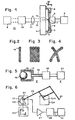
- FIG. 1 which is not drawn to scale, 1 means a flat, rigid and optically transparent printing plate.
- An optically transparent substrate 2 is attached to this in a manner not shown in detail.
- the surface of the substrate 2 facing away from the printing plate 1 is coated with a thin layer 3 of thermoplastic, radiation-absorbing material, into which a macroscopic surface pattern with a microscopic structure, in particular a structure with an optical diffraction effect, is to be embossed.
- Layer 3 may e.g. B. consist of a black or colored plastic film. You can also by coloring the surface of the substrate 2 z. B. be formed by means of colloidal carbon in a plastic solution. Their typical thickness is 0.1 to 10 ⁇ m.
- An unheated embossing die 4 is arranged opposite the thermoplastic layer 3 and has the microstructure to be molded in zones, e.g. B. consists of a nickel alloy and is advantageously so flexible that a stamp 5 can be used to generate a narrowly limited embossing pressure between the embossing die 4 and the thermoplastic layer 3.
- the typical thickness of the embossing die is 100 J.1m.
- the punch 5 advantageously has a convex surface with a typical radius of curvature of about 7 mm.
- the stamp 5 is pressed onto the embossing die 4 by means of a pressure transmitter 6 and this is pressed onto the thermoplastic layer 3 in the region of a small contact zone 7, the typical diameter of which is 3 mm.
- Die holder 8 holds the embossing die 4 such that it rests on the thermoplastic layer 3 only in the area of the contact zone 7 and is otherwise slightly distanced from it.
- the die holder 8 is advantageously designed such that the embossing die 4 can be rotated in a few simple steps or even mechanically or can be replaced by another embossing die with a different microstructure when the pressure transmitter 6 is in the rest position.
- a radiation source 12 Arranged on the side of the printing plate 1 facing away from the embossing die 4 is a radiation source 12 which advantageously consists of a laser 9, an optical modulator 10 and a lens system 11 and which focuses a bundled heat or light beam 13 onto a focal spot 14 in the region of the thermoplastic layer 3 , which lies approximately in the center of the contact zone 7.
- the layer 3 is heated in the area of the focal spot 14 by absorption of the directly incident beam 13 and the beam reflected on the embossing die 4.
- the typical diameter of the focal spot 14 is less than 100 ⁇ m.
- the energy of the heat or light beam 13 can be controlled or switched on and off with the aid of the modulator 10.
- the pressure transmitter 6 allows the plunger 5 to be adjusted in the z-axis, which is perpendicular to the surface of parts 1 to 4.
- the described components of the device are mounted on a base plate (not shown) in such a way that the pressure plate 1, the substrate 2 with the thermoplastic layer 3 and the embossing die 4 relative to the focal spot 14 and stamp 5 both in the x-axis and in the y- Axis, d. H. in a plane parallel to the thermoplastic layer 3, continuously or stepwise can be shifted against each other.
- parts 1 to 4 can be moved and parts 5 and 12 can be mounted in a fixed position, or vice versa. It is also possible to arrange the parts 1 to 4 and 12 in a stationary manner and to track the beam 12 by means of a mirror system of the movement of the stamp 5 in the x-y plane.
- the embossing pressure is adjusted with the aid of the pressure sensor 6 so that the thermoplastic layer 3, in its cold state in the region of the contact zone 7, only adjusts elastically to the microstructure of the embossing die 4 and, when the embossing pressure is released, returns to the original, e.g. B. relaxed state relaxed.
- the radiation-absorbing thermoplastic layer 3 is heated above the softening temperature in an approximately punctiform surface element, which lies in the focal spot 14 of the radiation source 12, so that its surface element in this surface element corresponds to the microstructure the embossing die 4 is plastically deformed and the embossed structure is retained after cooling when the embossing pressure is released.
- the desired surface pattern is now composed of a large number of such surface elements.
- the beam 13 is only switched on for a short time.
- the heated volume of the thermoplastic layer 3 then cools rapidly by thermal conduction into the embossing die 4 and the stamp 5 on the one hand and into the layer 3 or the substrate 2 on the other hand.
- the pressure transmitter 6 brings the stamp 5 into the rest position and thus separates the embossing die 4 from the thermoplastic layer 3.
- the embossed structure is retained in the area of the focal spot 14.
- This embossing process is now repeated successively by shifting the substrate 2 with its thermoplastic layer 3 relative to the focal spot 14 and stamp 5 in the x-y plane by a certain amount in a certain direction between the individual embossments with the radiation source 12 switched off and the embossing pressure removed.
- the embossing die 4 can be exchanged between the individual embossments or rotated by a certain amount about the z-axis. As a result, contiguous or isolated areas of layer 3 can be provided with any microscopic structures.
- the embossing die 4 and the substrate 2 with the layer 3 are continuously shifted at a certain speed relative to the focal spot 14 and the stamp 5 with the radiation source 12 and the pressure transmitter 6 switched on, so that coherent band-shaped surface areas of the microstructure of the embossing die 4 are molded.
- any surface pattern with a microscopic structure can be created by successive molding.
- the macroscopic surface patterns generated by the described method can represent geometric figures, numbers, letters, ornaments, guilloches, etc., the micro-tropical structure of which forms a single or a multiplicity of different phase diffraction gratings, phase holograms, kinoforms and the like.
- the thermoplastic layer 3 it is possible, in the thermoplastic layer 3, to economically produce a complex network of intertwined macroscopic lines with a diffractive optically effective microscopic structure, the microscopic structures changing from line to line or even along a line z.
- B. vary quasi-continuously so that the human eye has the effect of colored moving guilloche patterns.
- the described method can also be used, for example, to produce finely contoured microstructures, such as those used in the field of so-called integrated optics.
- the surface pattern generated on the thermoplastic layer 3 can be used according to known chemical and galvanic processes Duplicate be produced in the form of a metal embossing die, which is used for mass reproduction of the surface pattern in a conventional embossing device.
- the structure of the band forms e.g. B. a linear phase diffraction grating with 10 to 2000 lines per millimeter.
- a generated structure can be rewritten.
- the old structure is deleted if the energy density of the beam is sufficiently large. This simplifies the generation of complex structures, since in a first write operation it is not necessary to leave out those surface areas which are to be occupied with another structure in a subsequent second write operation.
- embossing pressure is generated by means of the stamp 5 exclusively in the area of the focal spot 14, then undesired partial cold deformations of the layer 3 upon pressure contact with the embossing die 4 at locations where the microstructure of the embossing die 4 is not to be molded, occur during the total embossing time in terms of duration and frequency reduced to what is absolutely necessary. Furthermore, the die change is made easier and, compared to the full-surface pressure generation, significantly smaller embossing forces result, which facilitates the mechanical design of the device.
- FIG. 5 shows a stamp 5 ', which consists of a ball holder 15 and a ball 16.
- the ball 16 lies with little play in a cylindrical space 17 of the ball holder 15.
- the longitudinal axis of the cylindrical space 17 coincides with the z-axis (FIG. 1).
- a part of the ball 16 protrudes from the ball holder 15 and forms the convex surface of the stamp 5 '.
- the space 17 is connected via a compressed air line 18 and a solenoid valve 19 to a compressed air source 20 acting as a pressure transmitter 6 '.
- the air overpressure in the space 17 presses the ball 16 against the embossing die 4 (FIG. 1 can be switched on and off by the solenoid valve 19 and can be varied within wide limits, which allows an exact adjustment of the embossing pressure.
- the automatic switching off of the embossing pressure by the solenoid valve 19 enables the embossing die 4 to be exchanged, rotated or moved in a simple manner.
- the lateral air bearing of the ball 16 ensures a low rolling resistance.
- the leakage air that escapes between the ball 16 and the cylindrical walls of the ball guide results in air cooling of the ball 16 .
- 21 means a graphic template, the macroscopic surface pattern 22 of which is scanned by means of an optoelectronic scanner 23 and reproduced to scale as a macroscopic surface pattern with a microscopic structure on layer 3 (FIG. 1).
- a displacement unit 24 guides the scanner 23 consisting of the light source, lens system and light detector (not shown).
- B. line by line via the template 21.
- the focal spot 14 and the stamp 5 are shifted relative to the layer 3 and the embossing die 4. In the drawing, this is indicated by a lever system in the form of a pantograph 25, which is moved by the displacement unit 24 and is thereby rotated about a fixed pivot point 26.
- the electrical output of the scanner 23 is connected via an amplifier 27 and a threshold switch 28 to a control input 29 of the modulator 10 of the radiation source 12.
- the modulator 10 is opened, so that the microstructure of the embossing die 4 is molded at the corresponding points in the layer 3.
- the predetermined value lying reflectivity on the other hand, there is neither a permanent impression of the microstructure nor a deletion of any structure previously shaped.
- the modulator 10 can also be controlled in such a way that embossing does not take place with high, but with low reflectivity of the pattern template 21. Furthermore, the modulator 10 can be controlled gradually instead of binary, the dependence of the energy of the beam 13 on the reflectivity of the template 21 being linear or non-linear. The gradual activation of the modulator 10 results in a modulation of the width of the embossed surface elements.
Description
- Die Erfindung bezieht sich auf ein Verfahren zur Erzeugung eines makroskopischen Flächenmusters mit einer mikroskopischen Struktur der im Oberbegriff des Anspruchs 1 genannten Art sowie auf eine Vorrichtung zur Durchführung des Verfahrens.
- Solche Flächenmuster dienen beispielsweise als beugungsoptisches Sicherheitselement auf einem Dokument (EP-A-0 105 099). Sie können als geometrische Figur, Zahl, Buchstabe, Ornament, Guilloche usw. ausgebildet und z. B. durch Aneinanderreihen einer grossen Zahl beugungsoptischer Elemente zusammengesetzt sein. Diese Synthese lässt sich dadurch realisieren, dass beugungsoptische Strukturen durch interferometrische Überlagerung kohärenter Lichtstrahlen mit unterschiedlichen Einfallswinkeln erzeugt werden, die photolithographisch in ein Oberflächenmikroprofil umgesetzt werden (EP-A-0 105 099), wobei zur geometrischen Begrenzung der zu belichtenden Felder feste vorfabrizierte optische Masken verwendet werden können. Wenn das zu erzeugende Flächenmuster und seine mikroskopische Struktur einen bestimmten Grad an graphischer und struktureller Komplexität überschreitet, erweist sich die Maskentechnik als prohibitiv aufwendig. Ausserdem lassen sich beugungsoptische Strukturelemente mit asymmetrischem Profil, z. B. spezielle Sägezahnprofile, durch die genannte interferometrische Methode nicht erzeugen.
- Es ist bekannt, beugungsoptisch wirksame Strukturen wie Phasenbeugungsgitter, Phasenhologramme und dergleichen durch Prägen in ein thermoplastisches Substrat mittels einer Prägematrize unter Anwendung von Druck und Wärme zu erzeugen (CH-PS 594495). Die Synthese eines Flächenmusters mit beugungsoptisch wirksamer Struktur könnte daher auch dadurch erfolgen, dass durch wiederholtes Prägen in ein thermoplastisches Substrat zahlreiche Phasenbeugungselemente aneinandergereiht werden. Diese Methode führt jedoch zu unbefriedigenden Resultaten, weil sich einerseits an den Prägerändern zwischen geheizter Druckzone und ungeheizter druckloser Fläche ausserhalb des Prägebereiches störende Wülste ergeben und andererseits die verschiedenen Prägezonen nicht nahtlos aneinandergelegt werden können, da infolge der grossen thermischen Masse metallischer Prägematrizen am Rand einer neuen Prägung die Randzone der benachbarten alten Prägung zwangsläufig gelöscht wird.
- Aus der CH-PS 594 495 ist es auch bekannt, auswählbare Bereiche einer eine Mikrostruktur aufweisenden Prägematrize dadurch abzuformen, dass die Prägematrize nur lokal aufgeheizt oder nur lokal auf das thermoplastische Substrat gepresst wird. Dabei entstehen jedoch keine scharf definierten Grenzen zwischen geprägten und ungeprägten Partien.
- Der Erfindung liegt die Aufgabe zugrunde, ein Verfahren der im Oberbegriff des Anspruchs 1 genannten Art sowie eine Vorrichtung anzugeben, die es gestatten, durch Abformen ausgewählter Flächenbereiche einer eine Mikrostruktur aufweisenden Prägematrize auf ökonomische Weise ein Flächenmuster mit einer mikroskopischen Struktur zu schaffen, bei dem die Prägeränder scharf begrenzt sind und keine störenden Wülste aufweisen.
- Die Verfahrenserfindung ist im Anspruch 1, die Vorrichtungserfindung ist im Anspruch 8 gekennzeichnet. Vorteilhafte Weiterbildungen ergeben sich aus den Unteransprüchen.
- Nachfolgend werden Ausführungsbeispiele der Erfindung anhand der Zeichnung näher erläutert.
- Es zeigen: Fig. 1 eine Prinzipdarstellunleiner
- Vorrichtung zur Erzeugung eines
- Flächenmusters,
- Fig. 2 bis 4 verschiedene
- Flächenmuster,
- Fig. 5 einen Stempel und
- Fig. 6 eine Prinzipdarstellung einer
- Vorrichtung zum Abtasten einer
- Mustervorlage.
- In der nicht maßstäblich gezeichneten Fig. 1 bedeutet 1 eine ebene, starre und optisch transparente Druckplatte. Auf dieser ist auf nicht näher dargestellte Weise ein optisch transparentes Substrat 2 befestigt. Die der Druckplatte 1 abgewandte Oberfläche des Substrates 2 ist mit einer dünnen Schicht 3 aus thermoplastischem, strahlungsabsorbierendem Material beschichtet, in welche ein makroskopisches Flächenmuster mit einer mikroskopischen Struktur, insbesondere einer beugungsoptisch wirksamen Struktur, eingeprägt werden soll. Die Schicht 3 kann z. B. aus einer schwarz oder farbig eingefärbten Kunststoffolie bestehen. Sie kann auch durch Einfärben der Oberfläche des Substrates 2 z. B. mittels kolloidalen Kohlenstoffes in einer Kunststofflösung gebildet werden. Ihre typische Dicke beträgt 0,1 bis 10 um.
- Gegenüber der thermoplastischen Schicht 3 ist eine ungeheizte Prägematrize 4 angeordnet, die die zonenweise abzuformende Mikrostruktur aufweist, z. B. aus einer Nickellegierung besteht und vorteilhaft derart flexibel ist, dass mittels eines Stempels 5 ein flächenmässig eng begrenzter Prägedruck zwischen der Prägematrize 4 und der thermoplastischen Schicht 3 erzeugt werden kann. Die typische Dicke der Prägematrize beträgt 100 J.1m. Vorteilhaft weist der Stempel 5 eine konvexe Oberfläche mit einem typischen Krümmungsradius von etwa 7 mm auf. Mittels eines Druckgebers 6 wird der Stempel 5 auf die Prägematrize 4 und diese im Bereich einer kleinen Kontaktzone 7, deren typischer Durchmesser 3 mm beträgt, auf die thermoplastische Schicht 3 gepresst. Ein in der Fig. 1 nur schematisch angedeuteter Matrizenhalter 8 hält die Prägematrize 4 so, dass diese nur im Bereich der Kontaktzone 7 auf der thermoplastischen Schicht 3 aufliegt und im übrigen von dieser leicht distanziert ist. Der Matrizenhalter 8 ist vorteilhaft derart ausgebildet, dass die Prägematrize 4 mit wenigen einfachen Handgriffen oder sogar maschinell verdreht oder durch eine andere Prägematrize mit unterschiedlicher Mikrostruktur ersetzt werden kann, wenn sich der Druckgeber 6 in der Ruhelage befindet.
- Auf der der Prägematrize 4 abgewandten Seite der Druckplatte 1 ist eine vorteilhaft aus einem Laser 9, einem optischen Modulator 10 und einem Linsensystem 11 bestehende Strahlenquelle 12 angeordnet, die einen gebündelten Wärme- oder Lichtstrahl 13 auf einen Brennfleck 14 im Bereich der thermoplastischen Schicht 3 fokussiert, der etwa im Zentrum der Kontaktzone 7 liegt. Durch Absorption des direkt einfallenden Strahls 13 und des an der Prägematrize 4 reflektierten Strahls wird die Schicht 3 im Bereich des Brennflecks 14 erhitzt. Der typische Durchmesser des Brennflecks 14 beträgt weniger als 100 um. Mit Hilfe des Modulators 10 lässt sich der Wärme-oder Lichtstrahl 13 in seiner Energie steuern bzw. ein- und ausschalten.
- Der Druckgeber 6 gestattet eine Verstellung des Stempels 5 in der z-Achse, die senkrecht zur Oberfläche der Teile 1 bis 4 liegt. Die beschriebenen Bauteile der Vorrichtung sind auf einer nicht dargestellten Grundplatte derart montiert, dass die Druckplatte 1, das Substrat 2 mit der thermoplastischen Schicht 3 und die Prägematrize 4 relativ zum Brennfleck 14 und Stempel 5 sowohl in der x-Achse als auch in der y-Achse, d. h. in einer zur thermoplastischen Schicht 3 parallelen Ebene, kontinuierlich oder schrittweise gegeneinander verschoben werden können. Hierzu können die Teile 1 bis 4 verschiebbar und die Teile 5 und 12 ortsfest montiert sein, oder umgekehrt. Es ist auch möglich, die Teile 1 bis 4 und 12 ortsfest anzuordnen und den Strahl 12 mittels eines Spiegelsystems der Bewegung des Stempels 5 in der x-y-Ebene nachzuführen.
- Der Prägedruck wird mit Hilfe des Druckgebers 6 so eingestellt, dass sich die thermoplastische Schicht 3 in ihrem kalten Zustand im Bereich der Kontaktzone 7 nur elastisch deformierend der Mikrostruktur der Prägematrize 4 anpasst und beim Nachlassen des Prägedruckes wieder in den ursprünglichen, z. B. glatten Zustand relaxiert. Wird hingegen gleichzeitig mit dem Prägedruck der Strahl 13 eingeschaltet, so wird die strahlungsabsorbierende thermoplastische Schicht 3 in einem annähernd punktförmigen Flächenelement, das im Brennfleck 14 der Strahlenquelle 12 liegt, über die Erweichungstemperatur so weit erhitzt, dass sich in diesem Flächenelement ihre Oberfläche entsprechend der Mikrostruktur der Prägematrize 4 plastisch verformt und die eingeprägte Struktur nach Abkühlung beim Nachlassen des Prägedruckes erhalten bleibt. Das gewünschte Flächenmuster wird nun aus einer Vielzahl solcher Flächenelemente zusammengesetzt.
- Im stationären Schreibmodus wird der Strahl 13 nur kurzzeitig eingeschaltet. Anschliessend kühlt sich das erhitzte Volumen der thermoplastischen Schicht 3 durch Wärmeleitung in die Prägematrize 4 und den Stempel 5 einerseits und in die Schicht 3 bzw. das Substrat 2 andererseits rasch ab. Der Druckgeber 6 bringt den Stempel 5 in die Ruhelage und trennt damit die Prägematrize 4 von der thermoplastischen Schicht 3. Im Bereich des Brennflecks 14 bleibt die eingeprägte Struktur erhalten. Nun wird dieses Prägeverfahren sukzessive wiederholt, indem zwischen den einzelnen Prägungen bei ausgeschalteter Strahlenquelle 12 und aufgehobenem Prägedruck das Substrat 2 mit seiner thermoplastischen Schicht 3 relativ zum Brennfleck 14 und Stempel 5 in der x-y-Ebene um einen bestimmten Betrag in einer bestimmten Richtung verschoben wird. Zwischen den einzelnen Prägungen kann die Prägematrize 4 ausgewechselt oder um einen bestimmten Betrag um die z-Achse verdreht werden. Dadurch lassen sich zusammenhängende oder voneinander isolierte Bereiche der Schicht 3 mit beliebigen mikroskopischen Strukturen versehen.
- Im dynamischen Schreibmodus werden die Prägematrize 4 und das Substrat 2 mit der Schicht 3 bei eingeschalteter Strahlenquelle 12 und eingeschaltetem Druckgeber 6 gegenüber dem Brennfleck 14 und dem Stempel 5 mit bestimmter Geschwindigkeit kontinuierlich verschoben, so dass zusammenhängende bandförmige Flächenbereiche der Mikrostruktur der Prägematrize 4 abgeformt werden. Auch im dynamischen Schreibmodus können durch sukzessives Abformen beliebige Flächenmuster mit mikroskopischer Struktur erzeugt werden.
- Die nach dem beschriebenen Verfahren erzeugten makroskopischen Flächenmuster können geometrische Figuren, Zahlen, Buchstaben, Ornamente, Guillochen usw. darstellen, deren mikrostropische Struktur ein einziges oder eine Vielzahl verschiedener Phasenbeugungsgitter, Phasenhologramme, Kinoforms und dergleichen bildet. So ist es beispielsweise möglich, in der thermoplastischen Schicht 3 auf ökonomische Weise ein komplexes Geflecht aus verschlungenen makroskopischen Linien mit beugungsoptisch wirksamer mikroskopischer Struktur zu erzeugen, wobei die mikroskopischen Strukturen von Linie zu Linie ändern oder sogar entlang einer Linie z. B. quasikontinuierlich variieren, so dass sich dem menschlichen Auge der Effekt von farbig bewegten Guillochenmustern ergeben. Das beschriebene Verfahren kann aber beispielsweise auch zur Erzeugung feinkonturierter Mikrostrukturen, wie sie im Gebiet der sog. Integrierten Optik Verwendung finden, angewandt werden.
- Von dem auf der thermoplastischen Schicht 3 erzeugten Flächenmuster kann nach bekannten chemischen und galvanischen Verfahren ein Duplikat in Form einer metallenen Prägematrize hergestellt werden, die zur Massenreproduktion des Flächenmusters in einer konventionellen Prägevorrichtung eingesetzt wird.
- Die Fig. 2 zeigt als einfaches Beispiel eines nach dem beschriebenen Verfahren hergestellten Flächenmusters ein schmales Band, das durch eine einzige Schreibbewegung in der y-Achse erzeugt wurde. Die Breite des Bandes ist etwa gleich oder wenig grösser als der Durchmesser des Brennflecks 14 und beträgt beispielsweise 50 J.1m. Die Struktur des Bandes bildet z. B. ein lineares Phasenbeugungsgitter mit 10 bis 2000 Linien pro Millimeter.
- Durch Aneinanderreihen solcher Bänder gemäss der Fig. 3 können Flächenmuster beliebiger Grösse erzeugt werden, wobei die mikroskopischen Strukturen benachbarter Bänder nahtlos ineinander übergehen. Werden mehrere solche Bänder nebeneinandergereiht, ohne dabei die Prägematrize 4 relativ zur Schicht 3 zu bewegen, so entsteht, wie aus der Fig. 3 ersichtlich ist, eine mikroskopische Struktur, deren Strukturlinien nahtlos über mehrere Bänder laufen.
- Gemäss der Fig. 4 kann eine erzeugte Struktur neu überschrieben werden. Dabei wird die alte Struktur gelöscht, falls die Energiedichte des Strahls genügend gross ist. Dies vereinfacht die Erzeugung komplexer Strukturen, da bei einem ersten Schreibvorgang nicht diejenigen Flächenbereiche ausgespart werden müssen, welche bei einem nachfolgenden zweiten Schreibvorgang mit einer anderen Struktur belegt werden sollen.
- Durch genaues Dosieren der Energiedichte des Strahls 13 und der Schreibgeschwindigkeit ist es aber auch möglich, eine neue Struktur über eine alte Struktur zu prägen, ohne dass dabei die alte Struktur vollständig gelöscht wird.
- Die Vorteile der Erfindung lassen sich nun leicht erkennen. Wie bereits erwähnt, können sowohl sehr feine linien- oder punktförmige Flächen als auch grössere zusammenhängende Flächenteile mit beugungsoptisch wirksamen Mikrostrukturen ohne sichtbare Nahtlinien durch Aneinanderschreiben oder teilweises Überschreiben belegt werden. Die Struktur der einzelnen Flächenelemente solcher Flächenmuster kann identisch sein oder von Element zu Element variieren. Es können auch Mikroprofile abgeformt werden, die sich durch interferometrische Methoden nicht erzeugen lassen. Die Prägeränder sind scharf begrenzt und weisen keine störenden Wülste auf. Generell ergibt sich durch das beschriebene Verfahren erstmals die Möglichkeit, feinkonturierte Mikrostrukturen frei von der Bindung an starre Maskensysteme zu synthetisieren, wobei der Verfahrensablauf durch numerische Programmierung und Steuerung vollständig automatisiert werden kann.
- Wird der Prägedruck mittels des Stempels 5 ausschliesslich im Bereich des Brennflecks 14 erzeugt, so werden unerwünschte partielle Kaltverformungen der Schicht 3 beim Druckkontakt mit der Prägematrize 4 an Stellen, wo die Mikrostruktur der Prägematrize 4 nicht abgeformt werden soll, während der Gesamtprägezeit bezüglich Dauer und Häufigkeit auf das unbedingt Notwendige reduziert. Ferner wird dadurch der Matrizenwechsel erleichtert und im Vergleich zur ganzflächigen Druckerzeugung ergeben sich wesentlich kleinere Prägekräfte, was die mechanische Auslegung der Vorrichtung erleichert.
- In der Fig. 5 ist ein Stempel 5' dargestellt, der aus einem Kugelhalter 15 und einer Kugel 16 besteht. Die Kugel 16 liegt mit geringem Spiel in einem zylindischen Raum 17 des Kugelhalters 15. Die Längsachse des zylindrischen Raumes 17 fällt mit der z-Achse (Fig. 1) zusammen. Ein Teil der Kugel 16 ragt aus dem Kugelhalter 15 heraus und bildet die konvexe Oberfläche des Stempels 5'. Der Raum 17 ist über eine Druckluftleitung 18 und ein Magnetventil 19 mit einer als Druckgeber 6' wirkenden Druckluftquelle 20 verbunden.
- Der Luftüberdruck im Raum 17 presst die Kugel 16 gegen die Prägematrize 4 (Fig. 1 kann durch das Magnetventil 19 ein- und ausgeschaltet werden und lässt sich in weiten Grenzen fein variieren, was eine genaue Justierung des Prägedrucks erlaubt. Die automatisierte Abschaltung des Prägedrucks durch das Magnetventil 19 ermöglicht auf einfache Weise das Auswechseln, Drehen oder Verschieben der Prägematrize 4. Die seitliche Luftlagerung der Kugel 16 gewährleistet einen geringen Rollwiderstand. Die Leckluft, die zwischen der Kugel 16 und den zylindrischen Wänden der Kugelführung entweicht, ergibt eine Luftkühlung der Kugel 16.
- In der Fig. 6 bedeutet 21 eine graphische Mustervorlage, deren makroskopisches Flächenmuster 22 mittels eines optoelektronischen Abtasters 23 abgetastet und als makroskopisches Flächenmuster mit mikroskopischer Struktur auf der Schicht 3 (Fig. 1) maßstabgetreu wiedergegeben wird. Eine Verschiebeeinheit 24 führt den aus Lichtquelle, Linsensystem und Lichtdetektor (nicht gezeichnet) bestehenden Abtaster 23 z. B. Zeile für Zeile über die Mustervorlage 21. Synchron dazu werden der Brennfleck 14 und der Stempel 5 gegenüber der Schicht 3 und der Prägematrize 4 verschoben. In der Zeichnung ist dies durch ein Hebelsystem in Form eines Pantographen 25 angedeutet, der durch die Verschiebeeinheit 24 bewegt und dabei um einen festen Drehpunkt 26 gedreht wird. Der elektrische Ausgang des Abtasters 23 ist über einen Verstärker 27 und einen Schwellenschalter 28 mit einem Steuereingang 29 des Modulators 10 der Strahlenquelle 12 verbunden.
- Übersteigt die lokale Reflektivität der Mustervorlage 21 einen vorbestimmten Wert, so wird der Modulator 10 geöffnet, so dass an den korrespondierenden Stellen der Schicht 3 die Mikrostruktur der Prägematrize 4 abgeformt wird. Bei unterhalb des vorbestimmten Wertes liegender Reflektivität erfolgt dagegen weder eine bleibende Abformung der Mikrostruktur noch eine Löschung einer allenfalls früher geprägten Struktur.
- Der Modulator 10 kann auch so gesteuert werden, dass eine Prägung nicht bei hoher, sondern bei geringer Reflektivität der Mustervorlage 21 stattfindet. Ferner kann der Modulator 10 graduell statt binär angesteuert werden, wobei die Abhängigkeit der Energie des Strahls 13 von der Reflektivität der Mustervorlage 21 linear oder nichtlinear sein kann. Die graduelle Ansteuerung des Modulators 10 ergibt eine Modulation der Breite der geprägten Flächenelemente.
Claims (10)
Priority Applications (1)
| Application Number | Priority Date | Filing Date | Title |
|---|---|---|---|
| AT85106087T ATE41250T1 (de) | 1984-07-06 | 1985-05-17 | Verfahren und vorrichtung zur erzeugung eines makroskopischen flaechenmusters mit einer mikroskopischen struktur, insbesondere einer beugungsoptisch wirksamen struktur. |
Applications Claiming Priority (2)
| Application Number | Priority Date | Filing Date | Title |
|---|---|---|---|
| CH3277/84 | 1984-07-06 | ||
| CH3277/84A CH664030A5 (de) | 1984-07-06 | 1984-07-06 | Verfahren zur erzeugung eines makroskopischen flaechenmusters mit einer mikroskopischen struktur, insbesondere einer beugungsoptisch wirksamen struktur. |
Publications (2)
| Publication Number | Publication Date |
|---|---|
| EP0169326A1 EP0169326A1 (de) | 1986-01-29 |
| EP0169326B1 true EP0169326B1 (de) | 1989-03-08 |
Family
ID=4252505
Family Applications (1)
| Application Number | Title | Priority Date | Filing Date |
|---|---|---|---|
| EP85106087A Expired EP0169326B1 (de) | 1984-07-06 | 1985-05-17 | Verfahren und Vorrichtung zur Erzeugung eines makroskopischen Flächenmusters mit einer mikroskopischen Struktur, insbesondere einer beugungsoptisch wirksamen Struktur |
Country Status (11)
| Country | Link |
|---|---|
| US (1) | US4761253A (de) |
| EP (1) | EP0169326B1 (de) |
| JP (1) | JPS6120723A (de) |
| AT (1) | ATE41250T1 (de) |
| AU (1) | AU572314B2 (de) |
| CA (1) | CA1266194A (de) |
| CH (1) | CH664030A5 (de) |
| DE (1) | DE3568651D1 (de) |
| DK (1) | DK160167C (de) |
| ES (1) | ES8702836A1 (de) |
| NO (1) | NO164401C (de) |
Cited By (1)
| Publication number | Priority date | Publication date | Assignee | Title |
|---|---|---|---|---|
| US8526085B2 (en) | 2007-08-22 | 2013-09-03 | Giesecke & Devrient Gmbh | Grid image |
Families Citing this family (68)
| Publication number | Priority date | Publication date | Assignee | Title |
|---|---|---|---|---|
| EP0330738B1 (de) * | 1988-03-03 | 1991-11-13 | Landis & Gyr Betriebs AG | Dokument |
| JP2789597B2 (ja) * | 1988-03-18 | 1998-08-20 | 凸版印刷株式会社 | ホログラム複製用多面付け原版の製造方法 |
| DE58909370D1 (de) * | 1988-09-30 | 1995-09-07 | Landis & Gry Tech Innovat Ag | Strichkodefeld und Strichkodeleser. |
| JP2564638B2 (ja) * | 1988-12-30 | 1996-12-18 | 太陽誘電株式会社 | コンパクトディスクの製造方法 |
| EP0537439B2 (de) * | 1991-10-14 | 2003-07-09 | OVD Kinegram AG | Sicherheitselement |
| US5538753A (en) * | 1991-10-14 | 1996-07-23 | Landis & Gyr Betriebs Ag | Security element |
| US6219015B1 (en) * | 1992-04-28 | 2001-04-17 | The Board Of Directors Of The Leland Stanford, Junior University | Method and apparatus for using an array of grating light valves to produce multicolor optical images |
| DE69421519D1 (de) * | 1994-04-08 | 1999-12-09 | Enea Ente Nuove Tec | Verfahren und Gerät für die Herstellung von Beugungsgittern in schnellem Bearbeitungssystem |
| ATE170014T1 (de) * | 1995-05-05 | 1998-09-15 | Landis & Gyr Tech Innovat | Verfahren zum aufbringen eines sicherheitselementes auf ein substrat |
| US5841579A (en) * | 1995-06-07 | 1998-11-24 | Silicon Light Machines | Flat diffraction grating light valve |
| US5661592A (en) * | 1995-06-07 | 1997-08-26 | Silicon Light Machines | Method of making and an apparatus for a flat diffraction grating light valve |
| US5629801A (en) * | 1995-06-07 | 1997-05-13 | Silicon Light Machines | Diffraction grating light doubling collection system |
| US5798743A (en) * | 1995-06-07 | 1998-08-25 | Silicon Light Machines | Clear-behind matrix addressing for display systems |
| US6064404A (en) * | 1996-11-05 | 2000-05-16 | Silicon Light Machines | Bandwidth and frame buffer size reduction in a digital pulse-width-modulated display system |
| US5882770A (en) * | 1996-12-31 | 1999-03-16 | Makansi; Munzer | Rainbow and hologram images on fabrics |
| US5982553A (en) | 1997-03-20 | 1999-11-09 | Silicon Light Machines | Display device incorporating one-dimensional grating light-valve array |
| US6088102A (en) * | 1997-10-31 | 2000-07-11 | Silicon Light Machines | Display apparatus including grating light-valve array and interferometric optical system |
| US6271808B1 (en) | 1998-06-05 | 2001-08-07 | Silicon Light Machines | Stereo head mounted display using a single display device |
| US6130770A (en) | 1998-06-23 | 2000-10-10 | Silicon Light Machines | Electron gun activated grating light valve |
| US6101036A (en) | 1998-06-23 | 2000-08-08 | Silicon Light Machines | Embossed diffraction grating alone and in combination with changeable image display |
| US6215579B1 (en) | 1998-06-24 | 2001-04-10 | Silicon Light Machines | Method and apparatus for modulating an incident light beam for forming a two-dimensional image |
| US6303986B1 (en) | 1998-07-29 | 2001-10-16 | Silicon Light Machines | Method of and apparatus for sealing an hermetic lid to a semiconductor die |
| GB2365815B (en) * | 1999-01-22 | 2002-10-30 | Sony Corp | Manufacture of optical elements |
| JP4099887B2 (ja) * | 1999-01-22 | 2008-06-11 | ソニー株式会社 | 光学素子の製造方法、並びに光学素子製造用金型 |
| JP2000214884A (ja) | 1999-01-22 | 2000-08-04 | Olympus Optical Co Ltd | 音声記録装置 |
| DE19925175C1 (de) * | 1999-05-27 | 2000-05-25 | Jenoptik Jena Gmbh | Einrichtung und Verfahren zur Übertragung von Mikrostrukturen |
| US6589628B1 (en) | 2000-06-27 | 2003-07-08 | Omnova Solutions Inc. | Article having optical effects |
| US20050037143A1 (en) * | 2000-07-18 | 2005-02-17 | Chou Stephen Y. | Imprint lithography with improved monitoring and control and apparatus therefor |
| US7211214B2 (en) * | 2000-07-18 | 2007-05-01 | Princeton University | Laser assisted direct imprint lithography |
| TW571291B (en) * | 2001-01-31 | 2004-01-11 | Ibm | Mechanical data processing |
| US6707591B2 (en) | 2001-04-10 | 2004-03-16 | Silicon Light Machines | Angled illumination for a single order light modulator based projection system |
| US6747781B2 (en) | 2001-06-25 | 2004-06-08 | Silicon Light Machines, Inc. | Method, apparatus, and diffuser for reducing laser speckle |
| US6782205B2 (en) | 2001-06-25 | 2004-08-24 | Silicon Light Machines | Method and apparatus for dynamic equalization in wavelength division multiplexing |
| US6829092B2 (en) | 2001-08-15 | 2004-12-07 | Silicon Light Machines, Inc. | Blazed grating light valve |
| US6800238B1 (en) | 2002-01-15 | 2004-10-05 | Silicon Light Machines, Inc. | Method for domain patterning in low coercive field ferroelectrics |
| EP1331084B1 (de) * | 2002-01-25 | 2004-03-10 | Leister Process Technologies | Verfahren zum Abformen von Mikro- und Nanostrukturen |
| US6767751B2 (en) | 2002-05-28 | 2004-07-27 | Silicon Light Machines, Inc. | Integrated driver process flow |
| US6728023B1 (en) | 2002-05-28 | 2004-04-27 | Silicon Light Machines | Optical device arrays with optimized image resolution |
| US6822797B1 (en) | 2002-05-31 | 2004-11-23 | Silicon Light Machines, Inc. | Light modulator structure for producing high-contrast operation using zero-order light |
| EP1513689A1 (de) * | 2002-06-20 | 2005-03-16 | Obducat AB | Verfahren und vorrichtung zum übertragen eines musters |
| US6829258B1 (en) | 2002-06-26 | 2004-12-07 | Silicon Light Machines, Inc. | Rapidly tunable external cavity laser |
| US6714337B1 (en) | 2002-06-28 | 2004-03-30 | Silicon Light Machines | Method and device for modulating a light beam and having an improved gamma response |
| US6813059B2 (en) | 2002-06-28 | 2004-11-02 | Silicon Light Machines, Inc. | Reduced formation of asperities in contact micro-structures |
| JP2005535483A (ja) * | 2002-08-09 | 2005-11-24 | レオナード クルツ ゲーエムベーハー ウント コンパニー カーゲー | レーザー支援複製プロセス |
| DE10236597A1 (de) * | 2002-08-09 | 2004-02-19 | Leonhard Kurz Gmbh & Co. Kg | Laserunterstütztes Replizierverfahren |
| US6801354B1 (en) | 2002-08-20 | 2004-10-05 | Silicon Light Machines, Inc. | 2-D diffraction grating for substantially eliminating polarization dependent losses |
| US6712480B1 (en) | 2002-09-27 | 2004-03-30 | Silicon Light Machines | Controlled curvature of stressed micro-structures |
| US7194105B2 (en) * | 2002-10-16 | 2007-03-20 | Hersch Roger D | Authentication of documents and articles by moiré patterns |
| US7295717B2 (en) * | 2002-10-16 | 2007-11-13 | Ecole polytechnique fédérale de Lausanne (EPFL) | Synthesis of superposition images for watches, valuable articles and publicity |
| US7305105B2 (en) | 2005-06-10 | 2007-12-04 | Ecole polytechnique fédérale de Lausanne (EPFL) | Authentication of secure items by shape level lines |
| US7751608B2 (en) | 2004-06-30 | 2010-07-06 | Ecole Polytechnique Federale De Lausanne (Epfl) | Model-based synthesis of band moire images for authenticating security documents and valuable products |
| JP2005005245A (ja) * | 2002-11-08 | 2005-01-06 | Fuji Photo Film Co Ltd | 転写素材の転写方法、形状転写方法及び転写装置 |
| US6806997B1 (en) | 2003-02-28 | 2004-10-19 | Silicon Light Machines, Inc. | Patterned diffractive light modulator ribbon for PDL reduction |
| US6829077B1 (en) | 2003-02-28 | 2004-12-07 | Silicon Light Machines, Inc. | Diffractive light modulator with dynamically rotatable diffraction plane |
| US7245406B2 (en) * | 2003-09-17 | 2007-07-17 | Dai Nippon Printing Co., Ltd. | Method for forming fine concavo-convex patterns, method for producing optical diffraction structure, and method for copying optical diffraction structure |
| US7037458B2 (en) * | 2003-10-23 | 2006-05-02 | Intel Corporation | Progressive stamping apparatus and method |
| JP2005352334A (ja) * | 2004-06-14 | 2005-12-22 | Dainippon Printing Co Ltd | 光回折構造転写シート及びその製造方法 |
| JP4569185B2 (ja) * | 2004-06-15 | 2010-10-27 | ソニー株式会社 | フィルム構造体の形成方法及びフィルム構造体 |
| GB0426724D0 (en) | 2004-12-06 | 2005-01-12 | Rue De Int Ltd | Improved hologram |
| WO2007089770A2 (en) * | 2006-01-31 | 2007-08-09 | Polychromix Corporation | Hand-held ir spectrometer with a fixed grating and a diffractive mems-array |
| US7721843B1 (en) * | 2006-02-08 | 2010-05-25 | The United States Of America As Represented By The Secretary Of The Navy | Visual acoustic device |
| EP2104930A2 (de) | 2006-12-12 | 2009-09-30 | Evans & Sutherland Computer Corporation | System und methode zum ausgleichen des rgb-licht in einem monomodulator projektor |
| US8358317B2 (en) | 2008-05-23 | 2013-01-22 | Evans & Sutherland Computer Corporation | System and method for displaying a planar image on a curved surface |
| US8702248B1 (en) | 2008-06-11 | 2014-04-22 | Evans & Sutherland Computer Corporation | Projection method for reducing interpixel gaps on a viewing surface |
| US8077378B1 (en) | 2008-11-12 | 2011-12-13 | Evans & Sutherland Computer Corporation | Calibration system and method for light modulation device |
| US8351087B2 (en) * | 2009-06-15 | 2013-01-08 | Ecole Polytechnique Federale De Lausanne (Epfl) | Authentication with built-in encryption by using moire parallax effects between fixed correlated s-random layers |
| US9641826B1 (en) | 2011-10-06 | 2017-05-02 | Evans & Sutherland Computer Corporation | System and method for displaying distant 3-D stereo on a dome surface |
| TWI672212B (zh) * | 2016-08-25 | 2019-09-21 | 國立成功大學 | 奈米壓印組合體及其壓印方法 |
Family Cites Families (8)
| Publication number | Priority date | Publication date | Assignee | Title |
|---|---|---|---|---|
| US3170008A (en) * | 1961-03-14 | 1965-02-16 | Litton Systems Inc | Embossing process |
| US3262122A (en) * | 1963-05-01 | 1966-07-19 | Ibm | Thermoplastic memory |
| FR1603960A (de) * | 1967-09-11 | 1971-06-21 | ||
| US4064205A (en) * | 1974-07-02 | 1977-12-20 | Logetronics, Inc. | Method for making a printing plate from a porous substrate |
| CH594495A5 (de) * | 1976-05-04 | 1978-01-13 | Landis & Gyr Ag | |
| FR2401484A1 (fr) * | 1977-08-25 | 1979-03-23 | Landis & Gyr Ag | Dispositif d'empreinte d'hologrammes dans un support thermoplastique |
| JPS59111820A (ja) * | 1982-12-16 | 1984-06-28 | Matsushita Electric Ind Co Ltd | 光情報担体デイスクの製造方法 |
| AU4922485A (en) * | 1984-11-09 | 1986-05-15 | Canadian Patents And Development Limited | Optical interference authenticating device |
-
1984
- 1984-07-06 CH CH3277/84A patent/CH664030A5/de not_active IP Right Cessation
-
1985
- 1985-05-17 EP EP85106087A patent/EP0169326B1/de not_active Expired
- 1985-05-17 DE DE8585106087T patent/DE3568651D1/de not_active Expired
- 1985-05-17 AT AT85106087T patent/ATE41250T1/de not_active IP Right Cessation
- 1985-05-29 JP JP60114450A patent/JPS6120723A/ja active Granted
- 1985-06-27 CA CA000485573A patent/CA1266194A/en not_active Expired - Lifetime
- 1985-07-03 DK DK304085A patent/DK160167C/da not_active IP Right Cessation
- 1985-07-05 ES ES544893A patent/ES8702836A1/es not_active Expired
- 1985-07-05 NO NO852716A patent/NO164401C/no unknown
- 1985-07-08 AU AU44674/85A patent/AU572314B2/en not_active Expired
-
1987
- 1987-01-29 US US07/014,096 patent/US4761253A/en not_active Expired - Lifetime
Cited By (1)
| Publication number | Priority date | Publication date | Assignee | Title |
|---|---|---|---|---|
| US8526085B2 (en) | 2007-08-22 | 2013-09-03 | Giesecke & Devrient Gmbh | Grid image |
Also Published As
| Publication number | Publication date |
|---|---|
| JPH0423897B2 (de) | 1992-04-23 |
| NO852716L (no) | 1986-01-07 |
| NO164401C (no) | 1990-10-03 |
| DK160167C (da) | 1991-07-08 |
| EP0169326A1 (de) | 1986-01-29 |
| DK160167B (da) | 1991-02-04 |
| US4761253A (en) | 1988-08-02 |
| DE3568651D1 (en) | 1989-04-13 |
| DK304085D0 (da) | 1985-07-03 |
| CA1266194A (en) | 1990-02-27 |
| ATE41250T1 (de) | 1989-03-15 |
| AU4467485A (en) | 1986-01-09 |
| CH664030A5 (de) | 1988-01-29 |
| DK304085A (da) | 1986-01-07 |
| AU572314B2 (en) | 1988-05-05 |
| JPS6120723A (ja) | 1986-01-29 |
| NO164401B (no) | 1990-06-25 |
| ES8702836A1 (es) | 1987-01-16 |
| ES544893A0 (es) | 1987-01-16 |
Similar Documents
| Publication | Publication Date | Title |
|---|---|---|
| EP0169326B1 (de) | Verfahren und Vorrichtung zur Erzeugung eines makroskopischen Flächenmusters mit einer mikroskopischen Struktur, insbesondere einer beugungsoptisch wirksamen Struktur | |
| EP0330738B1 (de) | Dokument | |
| DE3742770A1 (de) | Mikro-/ultrafiltrationsmembranen mit definierter porengroesse durch bestrahlung mit gepulsten lasern und verfahren zur herstellung | |
| EP0329787A1 (de) | Verfahren und anordnung für die laserbehandlung eines gegenstandes | |
| DE3719200A1 (de) | Optische speicherplatte und verfahren zu ihrer herstellung | |
| DE4132476A1 (de) | Verfahren, bedruckstoff und einrichtung zur verfielfaeltigung von holographischen feinstrukturen und anderen beugungsgittern auf printprodukte | |
| WO2020216541A1 (de) | Verfahren und vorrichtung zur herstellung eines hologramms, hologramm sowie beleuchtungsvorrichtung für ein fahrzeug | |
| EP1526962A1 (de) | Laserunterstütztes replizierverfahren | |
| EP1331084B1 (de) | Verfahren zum Abformen von Mikro- und Nanostrukturen | |
| DE102019109437A1 (de) | Verfahren und Vorrichtung zur Herstellung eines computergenerierten Hologramms, Hologramm sowie Beleuchtungsvorrichtung für ein Fahrzeug | |
| WO2017148575A1 (de) | Prägeplatte, herstellungsverfahren und geprägtes sicherheitselement | |
| EP1526963A1 (de) | Laserunterst tztes replizierverfahren | |
| DE4338218C2 (de) | Verfahren zur Herstellung eines Hologrammes oder Beugungsgitters sowie danach hergestelltes Hologramm oder Beugungsgitter | |
| EP0843281B9 (de) | Vorrichtung zur Herstellung von Oberflächenstrukturen | |
| EP0786326A1 (de) | Verfahren und Vorrichtung zur Herstellung von optischen Linsen und optischen Linsenarrays | |
| DE4340107B4 (de) | Verfahren zur Herstellung eines Teils mit einer fein strukturierten konkaven Oberfläche | |
| EP2660074A1 (de) | Prägeverfahren und ein mittels des Prägeverfahrens hergestelltes Werkstück | |
| DE2556414A1 (de) | Verfahren zum bedrucken eines traegers mit zeichen | |
| EP0204378A1 (de) | Verfahren zur Herstellung einer beschreibbaren optischen Speicherplatte | |
| DE10250476A1 (de) | Laserunterstütztes Replizierverfahren | |
| EP2307930A1 (de) | Verfahren zur herstellung von mikrostrukturen in einem speichermedium | |
| CN85105065A (zh) | 具有微观结构的宏观表面图样的生成方法 |
Legal Events
| Date | Code | Title | Description |
|---|---|---|---|
| PUAI | Public reference made under article 153(3) epc to a published international application that has entered the european phase |
Free format text: ORIGINAL CODE: 0009012 |
|
| AK | Designated contracting states |
Designated state(s): AT BE DE FR GB IT NL SE |
|
| 17P | Request for examination filed |
Effective date: 19860214 |
|
| 17Q | First examination report despatched |
Effective date: 19880502 |
|
| GRAA | (expected) grant |
Free format text: ORIGINAL CODE: 0009210 |
|
| AK | Designated contracting states |
Kind code of ref document: B1 Designated state(s): AT BE DE FR GB IT NL SE |
|
| REF | Corresponds to: |
Ref document number: 41250 Country of ref document: AT Date of ref document: 19890315 Kind code of ref document: T |
|
| GBT | Gb: translation of ep patent filed (gb section 77(6)(a)/1977) | ||
| REF | Corresponds to: |
Ref document number: 3568651 Country of ref document: DE Date of ref document: 19890413 |
|
| ET | Fr: translation filed | ||
| ITF | It: translation for a ep patent filed |
Owner name: STUDIO JAUMANN |
|
| PLBE | No opposition filed within time limit |
Free format text: ORIGINAL CODE: 0009261 |
|
| STAA | Information on the status of an ep patent application or granted ep patent |
Free format text: STATUS: NO OPPOSITION FILED WITHIN TIME LIMIT |
|
| 26N | No opposition filed | ||
| ITTA | It: last paid annual fee | ||
| EAL | Se: european patent in force in sweden |
Ref document number: 85106087.1 |
|
| PGFP | Annual fee paid to national office [announced via postgrant information from national office to epo] |
Ref country code: SE Payment date: 19960510 Year of fee payment: 12 Ref country code: BE Payment date: 19960510 Year of fee payment: 12 Ref country code: AT Payment date: 19960510 Year of fee payment: 12 |
|
| PGFP | Annual fee paid to national office [announced via postgrant information from national office to epo] |
Ref country code: NL Payment date: 19960514 Year of fee payment: 12 |
|
| PG25 | Lapsed in a contracting state [announced via postgrant information from national office to epo] |
Ref country code: AT Effective date: 19970517 |
|
| PG25 | Lapsed in a contracting state [announced via postgrant information from national office to epo] |
Ref country code: SE Effective date: 19970518 |
|
| PG25 | Lapsed in a contracting state [announced via postgrant information from national office to epo] |
Ref country code: BE Effective date: 19970531 |
|
| BERE | Be: lapsed |
Owner name: LGZ LANDIS & GYR ZUG A.G. Effective date: 19970531 |
|
| PG25 | Lapsed in a contracting state [announced via postgrant information from national office to epo] |
Ref country code: NL Effective date: 19971201 |
|
| EUG | Se: european patent has lapsed |
Ref document number: 85106087.1 |
|
| NLV4 | Nl: lapsed or anulled due to non-payment of the annual fee |
Effective date: 19971201 |
|
| REG | Reference to a national code |
Ref country code: FR Ref legal event code: TP |
|
| REG | Reference to a national code |
Ref country code: GB Ref legal event code: 732E |
|
| REG | Reference to a national code |
Ref country code: GB Ref legal event code: IF02 |
|
| PGFP | Annual fee paid to national office [announced via postgrant information from national office to epo] |
Ref country code: DE Payment date: 20040218 Year of fee payment: 20 |
|
| PGFP | Annual fee paid to national office [announced via postgrant information from national office to epo] |
Ref country code: GB Payment date: 20040505 Year of fee payment: 20 |
|
| PGFP | Annual fee paid to national office [announced via postgrant information from national office to epo] |
Ref country code: FR Payment date: 20040519 Year of fee payment: 20 |
|
| PG25 | Lapsed in a contracting state [announced via postgrant information from national office to epo] |
Ref country code: GB Free format text: LAPSE BECAUSE OF EXPIRATION OF PROTECTION Effective date: 20050516 |
|
| REG | Reference to a national code |
Ref country code: GB Ref legal event code: PE20 |