EP0167410A2 - Optical scanning microscope - Google Patents
Optical scanning microscope Download PDFInfo
- Publication number
- EP0167410A2 EP0167410A2 EP85304821A EP85304821A EP0167410A2 EP 0167410 A2 EP0167410 A2 EP 0167410A2 EP 85304821 A EP85304821 A EP 85304821A EP 85304821 A EP85304821 A EP 85304821A EP 0167410 A2 EP0167410 A2 EP 0167410A2
- Authority
- EP
- European Patent Office
- Prior art keywords
- beams
- optical scanning
- scanning microscope
- sample
- optical
- Prior art date
- Legal status (The legal status is an assumption and is not a legal conclusion. Google has not performed a legal analysis and makes no representation as to the accuracy of the status listed.)
- Withdrawn
Links
- 230000003287 optical effect Effects 0.000 title claims abstract description 39
- 230000010363 phase shift Effects 0.000 claims abstract description 6
- 235000010627 Phaseolus vulgaris Nutrition 0.000 claims 1
- 244000046052 Phaseolus vulgaris Species 0.000 claims 1
- 238000005259 measurement Methods 0.000 description 8
- 230000008859 change Effects 0.000 description 7
- 239000000758 substrate Substances 0.000 description 6
- 230000004044 response Effects 0.000 description 5
- 230000004075 alteration Effects 0.000 description 4
- 238000012545 processing Methods 0.000 description 4
- 238000004458 analytical method Methods 0.000 description 3
- 238000013459 approach Methods 0.000 description 3
- 238000001514 detection method Methods 0.000 description 3
- 238000010586 diagram Methods 0.000 description 3
- 239000010408 film Substances 0.000 description 3
- 239000000463 material Substances 0.000 description 3
- 238000000386 microscopy Methods 0.000 description 3
- 238000012986 modification Methods 0.000 description 3
- 230000004048 modification Effects 0.000 description 3
- 101000802640 Homo sapiens Lactosylceramide 4-alpha-galactosyltransferase Proteins 0.000 description 2
- 102100035838 Lactosylceramide 4-alpha-galactosyltransferase Human genes 0.000 description 2
- 229910052782 aluminium Inorganic materials 0.000 description 2
- XAGFODPZIPBFFR-UHFFFAOYSA-N aluminium Chemical compound [Al] XAGFODPZIPBFFR-UHFFFAOYSA-N 0.000 description 2
- 230000008901 benefit Effects 0.000 description 2
- BJQHLKABXJIVAM-UHFFFAOYSA-N bis(2-ethylhexyl) phthalate Chemical compound CCCCC(CC)COC(=O)C1=CC=CC=C1C(=O)OCC(CC)CCCC BJQHLKABXJIVAM-UHFFFAOYSA-N 0.000 description 2
- 230000000694 effects Effects 0.000 description 2
- 238000005286 illumination Methods 0.000 description 2
- 238000004519 manufacturing process Methods 0.000 description 2
- 229910052751 metal Inorganic materials 0.000 description 2
- 239000002184 metal Substances 0.000 description 2
- 238000000034 method Methods 0.000 description 2
- 238000009659 non-destructive testing Methods 0.000 description 2
- 238000000399 optical microscopy Methods 0.000 description 2
- 238000000847 optical profilometry Methods 0.000 description 2
- 238000002310 reflectometry Methods 0.000 description 2
- 230000035945 sensitivity Effects 0.000 description 2
- 230000009466 transformation Effects 0.000 description 2
- VYPSYNLAJGMNEJ-UHFFFAOYSA-N Silicium dioxide Chemical compound O=[Si]=O VYPSYNLAJGMNEJ-UHFFFAOYSA-N 0.000 description 1
- XUIMIQQOPSSXEZ-UHFFFAOYSA-N Silicon Chemical compound [Si] XUIMIQQOPSSXEZ-UHFFFAOYSA-N 0.000 description 1
- 229910003069 TeO2 Inorganic materials 0.000 description 1
- 230000001594 aberrant effect Effects 0.000 description 1
- XKRFYHLGVUSROY-UHFFFAOYSA-N argon Substances [Ar] XKRFYHLGVUSROY-UHFFFAOYSA-N 0.000 description 1
- 229910052786 argon Inorganic materials 0.000 description 1
- 230000001427 coherent effect Effects 0.000 description 1
- 230000001934 delay Effects 0.000 description 1
- 230000007613 environmental effect Effects 0.000 description 1
- 238000002474 experimental method Methods 0.000 description 1
- 238000001914 filtration Methods 0.000 description 1
- 239000005350 fused silica glass Substances 0.000 description 1
- 239000011521 glass Substances 0.000 description 1
- 238000013383 initial experiment Methods 0.000 description 1
- 238000002955 isolation Methods 0.000 description 1
- 239000000203 mixture Substances 0.000 description 1
- 239000002245 particle Substances 0.000 description 1
- 230000010287 polarization Effects 0.000 description 1
- 230000035939 shock Effects 0.000 description 1
- LAJZODKXOMJMPK-UHFFFAOYSA-N tellurium dioxide Chemical compound O=[Te]=O LAJZODKXOMJMPK-UHFFFAOYSA-N 0.000 description 1
- 238000012360 testing method Methods 0.000 description 1
- 239000010409 thin film Substances 0.000 description 1
Images


Classifications
-
- G—PHYSICS
- G02—OPTICS
- G02B—OPTICAL ELEMENTS, SYSTEMS OR APPARATUS
- G02B21/00—Microscopes
- G02B21/0004—Microscopes specially adapted for specific applications
- G02B21/002—Scanning microscopes
-
- G—PHYSICS
- G01—MEASURING; TESTING
- G01J—MEASUREMENT OF INTENSITY, VELOCITY, SPECTRAL CONTENT, POLARISATION, PHASE OR PULSE CHARACTERISTICS OF INFRARED, VISIBLE OR ULTRAVIOLET LIGHT; COLORIMETRY; RADIATION PYROMETRY
- G01J9/00—Measuring optical phase difference; Determining degree of coherence; Measuring optical wavelength
- G01J9/04—Measuring optical phase difference; Determining degree of coherence; Measuring optical wavelength by beating two waves of a same source but of different frequency and measuring the phase shift of the lower frequency obtained
-
- G—PHYSICS
- G01—MEASURING; TESTING
- G01N—INVESTIGATING OR ANALYSING MATERIALS BY DETERMINING THEIR CHEMICAL OR PHYSICAL PROPERTIES
- G01N21/00—Investigating or analysing materials by the use of optical means, i.e. using sub-millimetre waves, infrared, visible or ultraviolet light
- G01N21/84—Systems specially adapted for particular applications
- G01N21/8422—Investigating thin films, e.g. matrix isolation method
-
- G—PHYSICS
- G01—MEASURING; TESTING
- G01N—INVESTIGATING OR ANALYSING MATERIALS BY DETERMINING THEIR CHEMICAL OR PHYSICAL PROPERTIES
- G01N21/00—Investigating or analysing materials by the use of optical means, i.e. using sub-millimetre waves, infrared, visible or ultraviolet light
- G01N21/84—Systems specially adapted for particular applications
- G01N21/88—Investigating the presence of flaws or contamination
- G01N21/95—Investigating the presence of flaws or contamination characterised by the material or shape of the object to be examined
Definitions
- This invention relates to an optical scanning microscope,- and more particularly to a phase sensitive optical scanning microscope.
- Nondestructive testing especially in fields such as manufacture of integrated circuits is becoming extremely important as the dimensions of features in integrated circuits approach one micron or less. Such nondestructive testing would provide quantitative measurements of the surface, profiles and near surface material properties of products used in the manufacture of circuits.
- both the thickness and the width of the film is examined for blemishes, foreign particles, flatness and to insure the film is properly bonded at all points to the material.
- Interference microscopy invloves the resloving of fringes to evaluate surface height; however, again the fringe maps are difficult to interpret.
- an optical scanning microscope characterised by means for focusing at least two optical beams on a sample under study, means for optically scanning one of said beams across the sample, and means for comparing the phases of the beams after reflection from the sample to determine the phase shift of the scanned beam relative to the other beam as representing surface variation on the sample.
- the microscope of the present invention can measure differences in height to a very precise degree, and in particular can measure thickness of films or the like or relative thicknesses to accuracy of less than one hundred angstroms.
- the microscope of the invention allows for scanning of the sample electronically in order to maximize the scanning accuracy and minimize the susceptibility to vibration or mechanical shock.
- a collimated light beam such as a laser beam impinges on an acousto-optic deflector such as a Bragg cell.
- An appropriate high frequency signal may be applied to an acoustic transducer on the Bragg cell to modulate the impinging light beam.
- the output of the Bragg cell comprises two beams: a portion of the impinging light beam which passes directly through the cell or diffraction grating, and a second deflected output beam whose frequency is shifted by the frequency of the applied signal.
- the deflected beam may be scanned across the surface, while the reference beam remains in place and serves as a phase reference.
- a second input light beam is applied to the diffraction grating, the two input beams lying in a plane which is essentially perpendicular to the direction of scanning of the one beam.
- This second input beam after passing through the diffraction grating, will provide two further beams which impinge on the surface.
- These two beams which are to serve as reference beams should therefore be focused on a known flat surface; alternatively, the size of these beams may be expanded so that their size is very large relative to any surface feature to be detected; or as a further alternative they may be-reflected fron a known stable reference surface.
- the surface reflection of these beams is detected at a separate photodetector; upon mixing with the scan beam, the reference can be used to accurately detect any changes in phase and amplitude, while canceling out variations due to changes in those due to changes in frequency of the modulating optical wave in the Bragg cell.
- a microscope which incorporates these internal references is largely insensitive to environmental vibrations which are a common problem in interferometers. Further, the information from the scan is obtained in a form which is directly compatible with digital processing. This advantage occurs because since both amplitude and phase are measured and detected; it is possible to take a Fourier transformation of the complex spatial variation.
- This analysis system can be used with or without a Fourier transformation processing to remove aberrant effects in the lateral dimensions of surface features such as line widths on integrated ciruits.
- the optical phase can be easily calibrated to yield the height of surface features.
- the scanning microscope can be used as a noncontacting optical profilometer which provides height information and width information similar to that obtained using a mechanical stylus profilometer but without damage to the sample and with greatly increased accuracy.
- the phase measurement provides height information and the amplitude measurement provides width information, but when the materials being measured are thick or have several layers, or the width of the feature to be measured in comparable to beam spot size the problem of measurement is much more complicated. In this case it is extremely helpful to have separate phase and amplitude information which can be processed digitally.
- the width of a metal strip on a fused quartz substrate when the width of the strip is comparable to a spot size of the beam. If the beam is scanned across the strip we obtain a curve of intensity as a function of position. It is difficult to judge whether we should take the distance between half the full intensity points or use some other criterion for the width of the strip.
- the response obtained is the convolution of the line spread function P(x) of the beam and the reflection function of the strip r(x), i.e. the response is Where * denotes convolution, and x is the spatial position along the substrate.
- the strip is of width D
- the Fourier transform of r(x) in the spatial domain is
- r 0 is the amplitude and phase reflectivity of the strip and 6(o) is a Dirac delta function corresponding to the transform of the reflectivity of the substrate.
- V(k) the spatial frequency response of the system is a product of the spatial frequency responses of the lens and the substrate, we can search for the zeros of the response of and from their spacing determine D.
- the result should be independednt of P(k) provided P(k) is finite for k larger than values of K for which .
- digital processing of the input signal can be very important for determining the width of substrate features, and for removing lens aberrations.
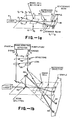
- the basic system as shown in Figure 1A utilizes a Bragg cell 2 such as already well known in the field of optics on which an output beam from a laser 4 or other source of highly collimated light impinges.
- the output of the Bragg cell consists of two beams.
- One beam 8 comprises a portion of the impinging beam at the same frequency f 0 passing directly through the Bragg cell.
- the other beam which is to be the scanned beam 10 passes out of the Bragg cell at a frequency f 0 plus f B .
- the frequency f B is the frequency of an input signal 12 which is applied to an adjacent face of the Bragg cell through a transducer to set up an acoustic wave through the Bragg cell which interacts with the impinging collimated light beam.
- the Bra gg cell 2 thus effectively acts as a diffraction grating, passing a portion of the beam through unimp ed - ed, and a second portion at a shifted frequency.
- the two beams are focused by a microscope objective lens 14 on the sample 16, the sample being located at the focal point of the objective lens.
- the laser 4 is a single frequency argon ion laser with etalon whose output is applied to a beam expander 20.
- the purpose of the beam expander is to provide an expanded beam of light; when the light passes through a microscope objective lens, the broad beam of light can be focused to an extremely small point by the objective lens.
- the reason for focusing a broad beam of light to a single point is to get the highest possible spatial resolution, which is especially important in examination of integrated circuits and the like.
- the beam of light is next passed through a Te0 2 Bragg cell 2 .
- This Bragg cell has a 60 to 110 Mhz swept frequency applied to a transducer attached to the edge of the cell from a voltage controlled oscillator.
- the light passing out of the Bragg cell as previously discussed is split into two beams 10, 8 with half of the light in each beam.
- the idea is to focus the light onto the sample through a microscope objective lens in two spots which are as small as possible.
- the back focal plane is actually within the mounting hardware of the microscope objective lens.
- a field lens 24 is provided for refocusing the two beams 8, 10 so that the Bragg cell image which is shown in dotted lines in the schematic diagram actually does appear to be at the back focal plane of the microscope objective lens as is apparent from the diagram, the sample is placed at the front focal plane of the same microscope objective lens.
- the distance f' is a value which depends on the numerical aperture which is in turn is defined by how steeply the light approaches the lens.
- One half of the beam passes directly out of the Bragg cell along the path 44, the other half leaves the Bragg cell along a Bragg angle path 46. Both of these beams are imaged on the sample 16 exactly as described above for the first laser beam through the microscope objective lens 14. These beams are reflected back, and combined and applied through a lens and detector to the phase sensitive detector electronics.
- the reference signal Since it is advantageous to detect phase at a fixed frequency, the reference signal is first limited and then single sideband modulated at an intermediate frequency of 60 MHz. Mixing this reference with the signal photodetector output gives a fixed frequency signal at 60 MHz which contains all the amplitude and phase information.
- the Rayleigh resolution is equal to that of the incoherent microscope, while the 3dB resolution is somewhat better, and the ripples observed while scanning across a discontinuity are reduced over that of a partially incoherent Type I system.
- the reference beams 44,46 are mixed in the photodiode to give a signal at 2f BJ the 2f B signal is single side band mixed with a 60 megahertz signal in a mixer 60; the reference beam and the actual scan signal beam are differenced; the combined signals are analyzed in a vector voltmeter 62 for the change in amplitude and change in phase information which reflects the changes in height and the width in such changes in the system.
- phase of the signal at 2f B depends on the optical path length difference between the two beams 8, 10 impinging on the sample 16, since the optical signals at frequencies f 0 + f B and f 0 - f B originate from the scan and stationery spots on the sample respectively.
- the theory on which this analysis is based is that for plane wave illumination, a surface height variation of h will introduce an optical phase change of 2kh as the beam in scanned over a feature of height h. For a tightly focused beam, the observed phase change is less since much of the incident light arrives at the sample at off-normal incidence.
- an electronic reference signal is required. Simply frequency doubling the Bragg cell drive signal is not sufficient since the finite acoustic delay in the Bragg cell will produce a large linear phase shift as the Bragg frequency is changed. Instead, a second optical signal is generated (Fig. lb) by splitting the beam incident on the Bragg cell in a direction perpendicular to the direction of acoustic wave propagation. Thus, four spots are focused on the sample. If the sample geometry is chosen so that the second set of spots is located on a uniform flat section of the sample, then they can be used for a reference. Alternatively, the second set of spots can be magnified to be much larger than the size of surface features of interest and placed anywhere on the sample, or reflected to a flat reference surface off the sample.
- Calibration scans are performed on an optically flat sample and amplitude and phase variations due to the electronics as well as optical aberrations are divided out and subtracted out, respectively. After this calibration, scans across a flat uniform sample show amplitude variations less than 3% and phase variations of less than 5°, suggesting a minimum surface height sensitivity of better than 50 ⁇ .
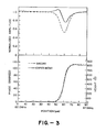
- Figure 3 demonstrates an initial experiment on the application of the microscope to optical profilometry.
- the aim was to eliminate phase changes due to the use of a wide aperture lens caused by polarization effects and changes in phase of the reflection coefficient.
- a step of aluminum 900A thick (as measured with a mechanical stylus) was 0 deposited on a glass substrate metallized with 500A of aluminum.
- a long focal length microscope objective (16 mm focal length) was illuminated with a narrow beam less than 1 mm in diameter. This yields an effective numerical aperture of less than 0.03.
- the Bragg cell frequency was scanned over the range of 82.0 MHz to 87.8 MHz, causing the focused beam to scan across 90 pm on the sample.
- the phase curve indicates a step height of 820 A, which is in fair agreement with the mechanical stylus measure-0 ment of 900 A, and demonstrates the ability to obtain good quantitative contrast on samples with features differing only in optical phase.
- the system described above provides an electronically-scanned optical microscope which can quantitatively measure amplitude and phase. Surface height variations can be accurately measured with the system.
- the ability to measure optical phase promises to make possible digital filtering to remove the the effect of aberrations and to accurately determine lateral dimensions on the sample.
Abstract
An optical scanning microscope utilises a Bragg cell (2) controlled by an input acoustic signal (12) to split a beam of light from a laser (4) into two beams (8, 10) which are focused onto a sample (16), one (10) of the beams being scanned across the sample (16) at the frequency of the input acoustic signal (12). The two beams (8, 10) are compared after reflection from the sample (16), the phase shift of the scanned beam (10) relative to the other beam (8) representing surface variation on the sample (16).
Description
- This invention relates to an
optical scanning microscope,- and more particularly to a phase sensitive optical scanning microscope. - Nondestructive testing, especially in fields such as manufacture of integrated circuits is becoming extremely important as the dimensions of features in integrated circuits approach one micron or less. Such nondestructive testing would provide quantitative measurements of the surface, profiles and near surface material properties of products used in the manufacture of circuits.
- This is especially important in the measurement of the thin films of metal that must be deposited on silicon chips. Ideally, both the thickness and the width of the film is examined for blemishes, foreign particles, flatness and to insure the film is properly bonded at all points to the material.
- Optical microscopy has been widely used as a method of evaluating small scale surface features. However, in fields where both the lateral dimensions and the height are of interest, conventional optical microscopy gives little quantitative information. It has been suggested in the past to use differential phase contrast to provide qualitative contrast for objects differing from their surroundings in optical phase rather than amplitude. However, it is apparent that it is very difficult to extract precise height information from such images.
- Interference microscopy invloves the resloving of fringes to evaluate surface height; however, again the fringe maps are difficult to interpret.
- According to the present invention there is provided an optical scanning microscope characterised by means for focusing at least two optical beams on a sample under study, means for optically scanning one of said beams across the sample, and means for comparing the phases of the beams after reflection from the sample to determine the phase shift of the scanned beam relative to the other beam as representing surface variation on the sample.
- The microscope of the present invention can measure differences in height to a very precise degree, and in particular can measure thickness of films or the like or relative thicknesses to accuracy of less than one hundred angstroms.
- In any such microscopy, it is extremely desirable to be able to scan the microscope across the surface in order to judge variations in height relative to a reference. This can be utilized both to determine the width of features, and to test the smoothness of surfaces and the success in bonding fils to surfaces.
- Earlier work done on optical profilometry using a differential technique or by heterodyning does not make use of or has not been able to successfully incorporate electronic scanning; therefore such systems had to rely on mechanical scanning. The microscope of the invention allows for scanning of the sample electronically in order to maximize the scanning accuracy and minimize the susceptibility to vibration or mechanical shock.
- With the scanning optical microscope of the invention a collimated light beam such as a laser beam impinges on an acousto-optic deflector such as a Bragg cell. An appropriate high frequency signal may be applied to an acoustic transducer on the Bragg cell to modulate the impinging light beam. The output of the Bragg cell comprises two beams: a portion of the impinging light beam which passes directly through the cell or diffraction grating, and a second deflected output beam whose frequency is shifted by the frequency of the applied signal. By modifying the frequency of the applied signal the deflected beam may be scanned across the surface, while the reference beam remains in place and serves as a phase reference. By detecting the two beams reflected from the surface, on a single photodetector, shifts in phase and amplitude of the scanned beam can be determined.
- In further modification which effectively incorporates an internal reference to provide significant further isolation of the system from external vibration, a second input light beam is applied to the diffraction grating, the two input beams lying in a plane which is essentially perpendicular to the direction of scanning of the one beam. This second input beam, after passing through the diffraction grating, will provide two further beams which impinge on the surface. These two beams which are to serve as reference beams, should therefore be focused on a known flat surface; alternatively, the size of these beams may be expanded so that their size is very large relative to any surface feature to be detected; or as a further alternative they may be-reflected fron a known stable reference surface. In any event, the surface reflection of these beams is detected at a separate photodetector; upon mixing with the scan beam, the reference can be used to accurately detect any changes in phase and amplitude, while canceling out variations due to changes in those due to changes in frequency of the modulating optical wave in the Bragg cell.
- A microscope which incorporates these internal references is largely insensitive to environmental vibrations which are a common problem in interferometers. Further, the information from the scan is obtained in a form which is directly compatible with digital processing. This advantage occurs because since both amplitude and phase are measured and detected; it is possible to take a Fourier transformation of the complex spatial variation. This analysis system can be used with or without a Fourier transformation processing to remove aberrant effects in the lateral dimensions of surface features such as line widths on integrated ciruits.
- On a sample of uniform composition, by use of the reference beam and deflected scanning beam, the optical phase can be easily calibrated to yield the height of surface features. By scanning the beam across the surface, the width and other dimensions of the surface features can also be accurately determined. Thus, the scanning microscope can be used as a noncontacting optical profilometer which provides height information and width information similar to that obtained using a mechanical stylus profilometer but without damage to the sample and with greatly increased accuracy. In its simplest embodiment the phase measurement provides height information and the amplitude measurement provides width information, but when the materials being measured are thick or have several layers, or the width of the feature to be measured in comparable to beam spot size the problem of measurement is much more complicated. In this case it is extremely helpful to have separate phase and amplitude information which can be processed digitally. As an example it can be difficult to measure the width of a metal strip on a fused quartz substrate, when the width of the strip is comparable to a spot size of the beam. If the beam is scanned across the strip we obtain a curve of intensity as a function of position. It is difficult to judge whether we should take the distance between half the full intensity points or use some other criterion for the width of the strip. By using amplitude and phase information, the response obtained is the convolution of the line spread function P(x) of the beam and the reflection function of the strip r(x), i.e. the response is

- The strip is of width D, the Fourier transform of r(x) in the spatial domain is

- Where r0 is the amplitude and phase reflectivity of the strip and 6(o) is a Dirac delta function corresponding to the transform of the reflectivity of the substrate. We can write


- This invention will now be described by way of example with reference to the drawings, in which:-
- Figure l(a) diagramatically illustrates a microscope in accordane with the invention;
- Figure l(b) illustrates a modification of the microscope of Figure l(a);
- Figure l(c) illustrates a further modification of the microscope of Figure l(a);
- Figure 2 is a block diagram of an analising circuit for use with the microscope fo Figure 1(b); and
- Figure 3 is a graph showing the results of a use of the microscope of the invention.
- The basic system as shown in Figure 1A utilizes a Bragg
cell 2 such as already well known in the field of optics on which an output beam from alaser 4 or other source of highly collimated light impinges. As a result of the impingement of the beam 6, at a frequency f0, the output of the Bragg cell consists of two beams. Onebeam 8 comprises a portion of the impinging beam at the same frequency f0 passing directly through the Bragg cell. The other beam which is to be the scannedbeam 10 passes out of the Bragg cell at a frequency f0 plus fB. The frequency fB is the frequency of aninput signal 12 which is applied to an adjacent face of the Bragg cell through a transducer to set up an acoustic wave through the Bragg cell which interacts with the impinging collimated light beam. - The Bragg cell 2 thus effectively acts as a diffraction grating, passing a portion of the beam through unimped- ed, and a second portion at a shifted frequency. The two beams are focused by a microscope objective lens 14 on the
sample 16, the sample being located at the focal point of the objective lens. In a preferred embodiment of the present invention shown in Fig. 1C, the laser 4 is a single frequency argon ion laser with etalon whose output is applied to abeam expander 20. The purpose of the beam expander is to provide an expanded beam of light; when the light passes through a microscope objective lens, the broad beam of light can be focused to an extremely small point by the objective lens. The reason for focusing a broad beam of light to a single point is to get the highest possible spatial resolution, which is especially important in examination of integrated circuits and the like. - The beam of light is next passed through a Te02 Bragg cell 2. This Bragg cell has a 60 to 110 Mhz swept frequency applied to a transducer attached to the edge of the cell from a voltage controlled oscillator. The light passing out of the Bragg cell as previously discussed is split into two
beams microscope objective lens 14, the back focal plane is actually within the mounting hardware of the microscope objective lens. Therefore, a field lens 24 is provided for refocusing the twobeams - The reflections of the two light beams travel back toward the Bragg cell along the same path as they followed in traveling toward the sample. Thus when the
scan beam 10 returns to the Bragg cell, it is again split in half, with half of the reflected signal going back toward the laser, and the other half traveling theanalysis path 30. In addition, half of thestationary beam 8 is reflected out of the Bragg cell at the Bragg angle along thedetection path 30. These beams which now have components f0 + fB and f0 - f respectively strike themirror 32 and pass through alens 34 andphoto detector 38 to the detection electronics. Apinhole 36 can be placed in front of the detector as a spatial filter. The output of the photodetection is at a frequency f 0 + f B - f 0 - f B = 2 fB - In order to provide a stable reference which indicates the frequency and phase of the swept frequency in the Bragg cell, it would be thought obvious to simply apply the 2nd harmonic of the
signal frequency 2fB to the detector electronics and use it as a phase reference. In fact, due to delays which occur in the acoustic signal as it passes across the Bragg cell, such a system would not provide sufficient phase accuracy. Therefore a further pair of reference beams are provided by applying a second laser beam of fixed frequency to the Bragg cell. Ideally, as shown in Figure 1B, in order that this second beam has exactly the same frequency and phase characteristics as the laser beam which provides the scannedbeam 10,beam splitter 40 is utilized to provide asecond beam 42, which in turn is separated into two components. One half of the beam passes directly out of the Bragg cell along thepath 44, the other half leaves the Bragg cell along aBragg angle path 46. Both of these beams are imaged on thesample 16 exactly as described above for the first laser beam through themicroscope objective lens 14. These beams are reflected back, and combined and applied through a lens and detector to the phase sensitive detector electronics. - It is important to note a second advantage derives from the use of coherent detection by mixing of two beams at the photo sensor. Specifically, the use of this type of detector provides a type II confocal point microscope (see G.S. Kino, Scanned Image Microscopy, E.A. Ash, Ed., Academic Press, London, Page 1, (1980)) which is scanned electronically across a surface. Such electronic scanning of a pin-point confocal microscope beam has never been previously achieved. Such scanning usually has been achieved in the prior art only by mechanical means. The photodiode detector is placed at the focus of a lens to compensate for the variation of the Bragg angle with frequency. Figure 2 shows the signal processing used to detect the amplitude and phase of the optically derived signals at 2fB. Since it is advantageous to detect phase at a fixed frequency, the reference signal is first limited and then single sideband modulated at an intermediate frequency of 60 MHz. Mixing this reference with the signal photodetector output gives a fixed frequency signal at 60 MHz which contains all the amplitude and phase information.
- In this configuration, the Rayleigh resolution is equal to that of the incoherent microscope, while the 3dB resolution is somewhat better, and the ripples observed while scanning across a discontinuity are reduced over that of a partially incoherent Type I system. Specif- ically, the reference beams 44,46 are mixed in the photodiode to give a signal at 2fBJ the 2fB signal is single side band mixed with a 60 megahertz signal in a
mixer 60; the reference beam and the actual scan signal beam are differenced; the combined signals are analyzed in avector voltmeter 62 for the change in amplitude and change in phase information which reflects the changes in height and the width in such changes in the system. This information is available because the phase of the signal at 2fB depends on the optical path length difference between the twobeams sample 16, since the optical signals at frequencies f0 + fB and f0 - fB originate from the scan and stationery spots on the sample respectively. The theory on which this analysis is based is that for plane wave illumination, a surface height variation of h will introduce an optical phase change of 2kh as the beam in scanned over a feature of height h. For a tightly focused beam, the observed phase change is less since much of the incident light arrives at the sample at off-normal incidence. By integrating over a uniformly illuminated spherical lens aperture, it can be shown that the feature introduces a phase change of
- To measure the phase shift in the interference signal at 2fB as the Bragg cell frequency fB is varied over the scan range, an electronic reference signal is required. Simply frequency doubling the Bragg cell drive signal is not sufficient since the finite acoustic delay in the Bragg cell will produce a large linear phase shift as the Bragg frequency is changed. Instead, a second optical signal is generated (Fig. lb) by splitting the beam incident on the Bragg cell in a direction perpendicular to the direction of acoustic wave propagation. Thus, four spots are focused on the sample. If the sample geometry is chosen so that the second set of spots is located on a uniform flat section of the sample, then they can be used for a reference. Alternatively, the second set of spots can be magnified to be much larger than the size of surface features of interest and placed anywhere on the sample, or reflected to a flat reference surface off the sample.
- Calibration scans are performed on an optically flat sample and amplitude and phase variations due to the electronics as well as optical aberrations are divided out and subtracted out, respectively. After this calibration, scans across a flat uniform sample show amplitude variations less than 3% and phase variations of less than 5°, suggesting a minimum surface height sensitivity of better than 50Å.
- In an experiment, 5mW from an etalon controlled single-frequency argon-ion laser at 510nm was used. The TeO2 Bragg cell has a bandwidth of 60-110MHz and deflection angles of 3° to 6°. Microscope objectives with numerical apertures in the range of 0.1 to .86 were used. The length of the scan on the sample is proportional to the frequency change times the objective focal length. With the higher numerical aperture, a 1/e2 spot radius of 1 µm was measured by examining the reflection from a metallized edge.
- Figure 3 demonstrates an initial experiment on the application of the microscope to optical profilometry. In order to check the system performance, the aim was to eliminate phase changes due to the use of a wide aperture lens caused by polarization effects and changes in phase of the reflection coefficient. A step of aluminum 900A thick (as measured with a mechanical stylus) was 0 deposited on a glass substrate metallized with 500A of aluminum. To simulate plane wave illumination, a long focal length microscope objective (16 mm focal length) was illuminated with a narrow beam less than 1 mm in diameter. This yields an effective numerical aperture of less than 0.03. The Bragg cell frequency was scanned over the range of 82.0 MHz to 87.8 MHz, causing the focused beam to scan across 90 pm on the sample. In Fig. 3, the amplitude and phase of the scanned spot are shown. After calibration, 5° of phase offset has been subtracted from the experimental phase curve. The theoretical curves are evaluated numerically for a Gaussian beam with a 1/e2 radius of 9µm, which in consistent with the small numerical aperture of the lens used. The beam is assumed to have constant optical phase and is convolved across the phase step. Due to aberrations and misfocusing, there may be phase variations across the beam which could account for the discrepancy between the experimental and theoretical amplitude curves.
- The phase curve indicates a step height of 820 A, which is in fair agreement with the mechanical stylus measure-0 ment of 900 A, and demonstrates the ability to obtain good quantitative contrast on samples with features differing only in optical phase.
- The system described above provides an electronically-scanned optical microscope which can quantitatively measure amplitude and phase. Surface height variations can be accurately measured with the system. In addition, the ability to measure optical phase promises to make possible digital filtering to remove the the effect of aberrations and to accurately determine lateral dimensions on the sample.
Claims (15)
1. An optical scanning microscope characterised by means (2,14) for focusing at least two optical beams (8,10) on a sample (16) under study, means (12) for optically scanning one (10) of said beams (8,10) across the sample (16), and means for comparing the phases of the beams after reflection from the sample (10) to determine the phase shift of the scanned beam (10) relative to the other beam (8) as representing surface variation on the sample (16).
2. An optical scanning microscope as claimed in Claim 1, characterised by a laser (4) for suppluing an input beam of collimated light form which said two beams (8,10) are derived.
3. An optical scanning microscope as claimed in Claim 1 or Claim 2, characterised in that said focussing means comprises a Bragg cell (2) responsive to the optical input beam (12).
4. An optical scanning microscope as claimed in Claim 3, characterised in the said focussing means comprises a diffraction grating (40) for splitting the input beam into said two output beams comprising an undiffracted beam (44) and a diffracted beam (46).
5. An optical scanning microscope as claimed in Claim 2, Claim 3 or Claim 4, characterised in that said input beam has a given frequency f0, said scanning means (12) comprising frequency shifiting means for modifying the frequency of one of said output beams to a frequency f0 + fB,fB being the acoustic output frequency of said scanning means (12).
6. An optical scanning microscope as claimed in any preceding claim, characterised by a microscope objective lens (14) arranged between said scanning means (2) and said sample (16) for focussing said beams (8,10) on the sample (16).
7. An optical scanning microscope as claimed in any preceding claim, characterised in that said comparing means comprise a photodetector means (38) for receiving said reflected beams, and means coupled to the output of said photodetector means for determining the phase shift of the scanned beam (10) relative to the other beam (8).
8. An optical scanning microscope as claimed in Claim 7, characterised in that said reflected beans return through said focussing means (2), there being means (36) for focussing said reflected beams on said photodetector means (38).
9. An optical scanning microscope as claimed in Claim 8, characterised by means (36) providing a pinhole opening for focussing said reflected beams on said photodetector means (38).
10. An optical scanning microscope as claimed in any preceding claim, characterised by means (40) for supplying first and second input beams to said focussing means (2), said focussing means (2) being responsive thereto to focus two additional beams (44, 46) on the sample (16).
11. An optical scanning microscope as claimed in Claim 10, characterised in that said first and second input beams lie in a plane perpendicular to the direction of scanning of said one (10) of said optical beams.
12. An optical scanning microscope as claimed in Claim 11, characterised by means for magnifying said two additional optical beams to a size larger than the sample area of interest.
13. An optical scanning microscope as claimed in Claim 12, characterised by means for comparing said first mentioned refected information bearing beams with said additonal reflected reference beams.
14. An optical scanning microscope as claimed in Claim 13, characterised by means (60) for mixing said reflected reference beam signal with a substantially higher intermediate signal frequency, and means for combining said mixed signal with said first mentioned reflected beam signal, said comparing means responding to said combining means to develop phase information.
15. An optical scanning microscope as claimed in Claim 14, characterised in that said comparing means further comprise means (62) responsive to said combining means to develop a signal indicating changes in amplitude in said scanned beam signal.
Applications Claiming Priority (2)
| Application Number | Priority Date | Filing Date | Title |
|---|---|---|---|
| US06/628,181 US4627730A (en) | 1984-07-06 | 1984-07-06 | Optical scanning microscope |
| US628181 | 1996-04-04 |
Publications (2)
| Publication Number | Publication Date |
|---|---|
| EP0167410A2 true EP0167410A2 (en) | 1986-01-08 |
| EP0167410A3 EP0167410A3 (en) | 1987-05-20 |
Family
ID=24517817
Family Applications (1)
| Application Number | Title | Priority Date | Filing Date |
|---|---|---|---|
| EP85304821A Withdrawn EP0167410A3 (en) | 1984-07-06 | 1985-07-05 | Optical scanning microscope |
Country Status (3)
| Country | Link |
|---|---|
| US (1) | US4627730A (en) |
| EP (1) | EP0167410A3 (en) |
| JP (1) | JPS61105522A (en) |
Cited By (6)
| Publication number | Priority date | Publication date | Assignee | Title |
|---|---|---|---|---|
| WO1988000683A1 (en) * | 1986-07-18 | 1988-01-28 | National Research Development Corporation | Microscopes |
| FR2626383A1 (en) * | 1988-01-27 | 1989-07-28 | Commissariat Energie Atomique | CONFOCAL CONFIGURED OPTICAL MICROSCOPY METHOD WITH SCAN AND DEPTH OF EXTENDED FIELD AND DEVICES FOR IMPLEMENTING THE METHOD |
| WO1989009380A1 (en) * | 1988-03-31 | 1989-10-05 | National Research Development Corporation | Optical measuring apparatus and method |
| US4890921A (en) * | 1986-08-11 | 1990-01-02 | The Boeing Company | Scanning interferometer |
| EP0444450A1 (en) * | 1990-03-02 | 1991-09-04 | International Business Machines Corporation | Latent-image control of lithography tools |
| WO1992003697A1 (en) * | 1990-08-20 | 1992-03-05 | British Technology Group Ltd | Optical apparatus |
Families Citing this family (14)
| Publication number | Priority date | Publication date | Assignee | Title |
|---|---|---|---|---|
| US4978219A (en) * | 1988-05-06 | 1990-12-18 | Brother Kogyo Kabushiki Kaisha | Surface roughness measuring apparatus utilizing deflectable laser beams |
| US5022757A (en) * | 1989-01-23 | 1991-06-11 | Modell Mark D | Heterodyne system and method for sensing a target substance |
| JPH04157415A (en) * | 1990-10-20 | 1992-05-29 | Fuji Photo Film Co Ltd | Confocal scanning type interference microscope |
| US5583643A (en) * | 1991-04-12 | 1996-12-10 | British Technology Group Ltd. | Methods of and apparatus for measurement using acousto-optic devices |
| GB9107796D0 (en) * | 1991-04-12 | 1991-05-29 | Nat Res Dev | Methods of and apparatus for measurement using acousto-optic devices |
| EP0789383B1 (en) | 1996-02-08 | 2008-07-02 | Canon Kabushiki Kaisha | Method of manufacturing electron-emitting device, electron source and image-forming apparatus and method of examining the manufacturing |
| US5694216A (en) * | 1996-04-25 | 1997-12-02 | University Of Central Florida | Scanning heterodyne acousto-optical interferometers |
| US5831736A (en) * | 1996-08-29 | 1998-11-03 | Washington University | Method and apparatus for generating a three-dimensional topographical image of a microscopic specimen |
| DE19936573A1 (en) | 1998-12-22 | 2001-02-08 | Zeiss Carl Jena Gmbh | Arrangement for the separation of excitation and emission light in a microscope |
| US7054504B2 (en) * | 1999-02-25 | 2006-05-30 | Ludwig Lester F | Relative optical path phase reconstruction in the correction of misfocused images using fractional powers of the fourier transform |
| US6943898B2 (en) * | 2002-05-07 | 2005-09-13 | Applied Materials Israel, Ltd. | Apparatus and method for dual spot inspection of repetitive patterns |
| FI20031143A0 (en) * | 2003-08-08 | 2003-08-08 | Wallac Oy | Optical Focusing Method and Arrangement |
| US20110032534A1 (en) * | 2009-05-19 | 2011-02-10 | Camtek Ltd | System and a method for broadband interferometry |
| EP3538941A4 (en) | 2016-11-10 | 2020-06-17 | The Trustees of Columbia University in the City of New York | Rapid high-resolution imaging methods for large samples |
Citations (4)
| Publication number | Priority date | Publication date | Assignee | Title |
|---|---|---|---|---|
| US4183671A (en) * | 1978-03-14 | 1980-01-15 | The United States Of America As Represented By The United States Department Of Energy | Interferometer for the measurement of plasma density |
| US4305666A (en) * | 1979-10-24 | 1981-12-15 | Massachusetts Institute Of Technology | Optical heterodyne detection system and method |
| EP0079276A1 (en) * | 1981-11-06 | 1983-05-18 | Commissariat A L'energie Atomique | Method and device for the measurement of the wave surface deformations introduced by an optical system |
| GB2146116A (en) * | 1983-05-13 | 1985-04-11 | Citizen Watch Co Ltd | Surface condition measurement apparatus |
Family Cites Families (3)
| Publication number | Priority date | Publication date | Assignee | Title |
|---|---|---|---|---|
| US3796495A (en) * | 1972-05-30 | 1974-03-12 | Zenith Radio Corp | Apparatus and methods for scanning phase profilometry |
| US4353650A (en) * | 1980-06-16 | 1982-10-12 | The United States Of America As Represented By The United States Department Of Energy | Laser heterodyne surface profiler |
| SE8300112L (en) * | 1982-01-16 | 1983-07-17 | Whiting Richard A | FOR USE IN A WINDOW, A DOOR OR OTHER THAN AS FRAMEWORK CONSTRUCTION DEVICE DEVICE LEMPAT, LONG STRENGTH FRAME ELEMENT |
-
1984
- 1984-07-06 US US06/628,181 patent/US4627730A/en not_active Expired - Fee Related
-
1985
- 1985-07-05 EP EP85304821A patent/EP0167410A3/en not_active Withdrawn
- 1985-07-06 JP JP60149082A patent/JPS61105522A/en active Pending
Patent Citations (4)
| Publication number | Priority date | Publication date | Assignee | Title |
|---|---|---|---|---|
| US4183671A (en) * | 1978-03-14 | 1980-01-15 | The United States Of America As Represented By The United States Department Of Energy | Interferometer for the measurement of plasma density |
| US4305666A (en) * | 1979-10-24 | 1981-12-15 | Massachusetts Institute Of Technology | Optical heterodyne detection system and method |
| EP0079276A1 (en) * | 1981-11-06 | 1983-05-18 | Commissariat A L'energie Atomique | Method and device for the measurement of the wave surface deformations introduced by an optical system |
| GB2146116A (en) * | 1983-05-13 | 1985-04-11 | Citizen Watch Co Ltd | Surface condition measurement apparatus |
Non-Patent Citations (3)
| Title |
|---|
| APPLIED OPTICS, vol. 8, no. 8, August 1969, pages 1567-1576, New York, US; R.L.WHITMAN et al. : "Probing of acoustic surface perturbations by coherent light" * |
| APPLIED PHYSICS LETTERS, vol. 45, no. 8, 15th October 1984, pages 846-848, American Institute of Physics, New York, US; R.L.JUNGERMAN et al.: "Phase sensitive scanning optical microscope" * |
| PROCEEDINGS OF THE IEE,,February 1972, vol. 119, no. 2, pages 117-126, Stevenage Herts; R.M.DE LA RUE et al. : "Acoustic-surface-wave amplitude and phase measurements using laser probes" * |
Cited By (13)
| Publication number | Priority date | Publication date | Assignee | Title |
|---|---|---|---|---|
| WO1988000683A1 (en) * | 1986-07-18 | 1988-01-28 | National Research Development Corporation | Microscopes |
| US4890921A (en) * | 1986-08-11 | 1990-01-02 | The Boeing Company | Scanning interferometer |
| FR2626383A1 (en) * | 1988-01-27 | 1989-07-28 | Commissariat Energie Atomique | CONFOCAL CONFIGURED OPTICAL MICROSCOPY METHOD WITH SCAN AND DEPTH OF EXTENDED FIELD AND DEVICES FOR IMPLEMENTING THE METHOD |
| EP0327425A1 (en) * | 1988-01-27 | 1989-08-09 | Commissariat A L'energie Atomique | Method for optical scanning microscopy in confocal arrangement with large depth of field and apparatus to perform this method |
| US4965441A (en) * | 1988-01-27 | 1990-10-23 | Commissariat A L'energie Atomique | Method for the scanning confocal light-optical microscopic and indepth examination of an extended field and devices for implementing said method |
| US5139336A (en) * | 1988-03-31 | 1992-08-18 | National Research Development Corporation | Optical measuring apparatus using amplitude modulation of slipt beams |
| WO1989009380A1 (en) * | 1988-03-31 | 1989-10-05 | National Research Development Corporation | Optical measuring apparatus and method |
| EP0444450A1 (en) * | 1990-03-02 | 1991-09-04 | International Business Machines Corporation | Latent-image control of lithography tools |
| US5124927A (en) * | 1990-03-02 | 1992-06-23 | International Business Machines Corp. | Latent-image control of lithography tools |
| GB2248500A (en) * | 1990-08-20 | 1992-04-08 | Nat Res Dev | Optical topographic measuring apparatus with a reference beam and a multi-frequency modulated probe beam |
| WO1992003697A1 (en) * | 1990-08-20 | 1992-03-05 | British Technology Group Ltd | Optical apparatus |
| US5369489A (en) * | 1990-08-20 | 1994-11-29 | British Technology Group Ltd. | Time division multiplexed microscopy |
| GB2248500B (en) * | 1990-08-20 | 1995-03-22 | Nat Res Dev | Optical apparatus |
Also Published As
| Publication number | Publication date |
|---|---|
| EP0167410A3 (en) | 1987-05-20 |
| US4627730A (en) | 1986-12-09 |
| JPS61105522A (en) | 1986-05-23 |
Similar Documents
| Publication | Publication Date | Title |
|---|---|---|
| US4627730A (en) | Optical scanning microscope | |
| US6087652A (en) | Contactless acoustic sensing system with detector array scanning and self-calibration | |
| US4633715A (en) | Laser heterodyne interferometric method and system for measuring ultrasonic displacements | |
| US6552799B1 (en) | Two-arm sagnac interferometer with two beam splitters | |
| US4966459A (en) | Broadband optical detection of transient motion from a scattering surface | |
| Dändliker | I Heterodyne Holographic Interferometry | |
| US4432239A (en) | Apparatus for measuring deformation | |
| US4422764A (en) | Interferometer apparatus for microtopography | |
| EP0650030B1 (en) | Apparatus for and method of evaluating multilayer thin films | |
| US4534649A (en) | Surface profile interferometer | |
| US4503708A (en) | Reflection acoustic microscope for precision differential phase imaging | |
| US5285261A (en) | Dual interferometer spectroscopic imaging system | |
| US7002695B2 (en) | Dual-spot phase-sensitive detection | |
| US6937343B2 (en) | Laser scanner with amplitude and phase detection | |
| Jungerman et al. | Phase sensitive scanning optical microscope | |
| US6552800B1 (en) | Single-arm sagnac interferometer with two beam splitters | |
| EP0407454B1 (en) | Optical measuring apparatus | |
| US5406377A (en) | Spectroscopic imaging system using a pulsed electromagnetic radiation source and an interferometer | |
| US6549285B1 (en) | Two-arm Sagnac interferometer with three beam splitters | |
| GB2109545A (en) | Surface profile interferometer | |
| US5008851A (en) | Optical heterodyning system and method for rapid optical phase and amplitude measurements | |
| US20030128366A1 (en) | Imaging systems | |
| EP0731335B1 (en) | Apparatus and method for non destructive testing of coherent radiation illuminated material | |
| KR102494082B1 (en) | Measuring apparatus for thickness and profile for thin film using interference and wavenumber high frequency modulation, and measuring method using thereof | |
| Hirai et al. | Heterodyne Fourier transform spectroscopy using moving diffraction grating |
Legal Events
| Date | Code | Title | Description |
|---|---|---|---|
| PUAI | Public reference made under article 153(3) epc to a published international application that has entered the european phase |
Free format text: ORIGINAL CODE: 0009012 |
|
| AK | Designated contracting states |
Designated state(s): AT CH DE FR GB LI |
|
| PUAL | Search report despatched |
Free format text: ORIGINAL CODE: 0009013 |
|
| AK | Designated contracting states |
Kind code of ref document: A3 Designated state(s): AT CH DE FR GB LI |
|
| STAA | Information on the status of an ep patent application or granted ep patent |
Free format text: STATUS: THE APPLICATION IS DEEMED TO BE WITHDRAWN |
|
| 18D | Application deemed to be withdrawn |
Effective date: 19871121 |
|
| RIN1 | Information on inventor provided before grant (corrected) |
Inventor name: JUNGERMAN, ROGER LEE Inventor name: KINO, GORDON STANLEY |