EP0167322A2 - Shadow memory system - Google Patents
Shadow memory system Download PDFInfo
- Publication number
- EP0167322A2 EP0167322A2 EP85304350A EP85304350A EP0167322A2 EP 0167322 A2 EP0167322 A2 EP 0167322A2 EP 85304350 A EP85304350 A EP 85304350A EP 85304350 A EP85304350 A EP 85304350A EP 0167322 A2 EP0167322 A2 EP 0167322A2
- Authority
- EP
- European Patent Office
- Prior art keywords
- data
- memory
- power
- main memory
- store
- Prior art date
- Legal status (The legal status is an assumption and is not a legal conclusion. Google has not performed a legal analysis and makes no representation as to the accuracy of the status listed.)
- Withdrawn
Links
Images


Classifications
-
- G—PHYSICS
- G06—COMPUTING; CALCULATING OR COUNTING
- G06F—ELECTRIC DIGITAL DATA PROCESSING
- G06F11/00—Error detection; Error correction; Monitoring
- G06F11/07—Responding to the occurrence of a fault, e.g. fault tolerance
- G06F11/16—Error detection or correction of the data by redundancy in hardware
- G06F11/20—Error detection or correction of the data by redundancy in hardware using active fault-masking, e.g. by switching out faulty elements or by switching in spare elements
- G06F11/2015—Redundant power supplies
-
- G—PHYSICS
- G06—COMPUTING; CALCULATING OR COUNTING
- G06F—ELECTRIC DIGITAL DATA PROCESSING
- G06F1/00—Details not covered by groups G06F3/00 - G06F13/00 and G06F21/00
- G06F1/26—Power supply means, e.g. regulation thereof
- G06F1/30—Means for acting in the event of power-supply failure or interruption, e.g. power-supply fluctuations
-
- G—PHYSICS
- G06—COMPUTING; CALCULATING OR COUNTING
- G06F—ELECTRIC DIGITAL DATA PROCESSING
- G06F11/00—Error detection; Error correction; Monitoring
- G06F11/07—Responding to the occurrence of a fault, e.g. fault tolerance
- G06F11/14—Error detection or correction of the data by redundancy in operation
- G06F11/1402—Saving, restoring, recovering or retrying
- G06F11/1415—Saving, restoring, recovering or retrying at system level
- G06F11/1441—Resetting or repowering
Definitions
- This invention relates to a volatile data store with a backup storage system which is operable during a main power source failure. More particularly the invention relates to a shadow memory system in which a shadow memory is continually updated to reflect changes in data stored by the main memory so that in the event of a power failure only a small portion of the main memory data need be stored using backup power.
- Another commonly used data protection approach is to rely exclusively upon a battery backup in the event of a power failure.
- the battery backup is used to preserve the integrity of stored data during a power failure.
- large data stores consume large amounts of power and practical limitations on battery backup energy capacity limit data preservation to a few hours. If a power failure lasts more than a few hours critical data will be lost.
- Another known battery backup alternative is to use battery power to "dump" volatile memory data into a nonvolatile memory such as a disk drive upon the occurrence of a power failure. Because of the large amount of energy required to preserve the data for a large memory, practical battery sizes limit preservation of data to one, or at most two, occurrences. Assuming that the backup batteries are rechargeable, it will typically take at least 24 hours to recharge them. However, it is not uncommon for power failures to occur in a rapid sequence of multiple failures and restarts. If more power failures occur than can be accommodated by the data preservation system, data will be lost.
- a data storage system in accordance with the invention includes a volatile main memory coupled to a host CPU through a memory controller and a host CPU bus, a bus monitor circuit, a usage monitor memory, a power supply subsystem with battery backup and a shadow memory subsystem coupled to replicate in nonvolatile storage data stored by the main memory.
- a volatile main memory coupled to a host CPU through a memory controller and a host CPU bus
- a bus monitor circuit coupled to replicate in nonvolatile storage data stored by the main memory.
- the bus monitor circuit is coupled to a main memory bus which provides data communication with the volatile main .. memory. Each time a write access is made to the main memory over the main memory bus, the bus monitor writes into the usage monitor memory an indication of the main memory access.
- a memory multiplexer alternately grants access to the usage monitor memory to the bus monitor circuit and to the shadow memory subsystem in repetitive cycles that occur with sufficient frequency to assure that the bus monitor circuit may access the usage monitor memory each time there is a write access to the main memory.
- the shadow memory subsystem repetitively accesses and sequentially reads the usage monitor memory during the times that it is granted access to the usage monitor memory by a memory multiplexer. As long as the shadow memory subsystem finds no indication of a main memory write, it merely reads the next sequential usage monitor memory location. However, if an indication of a main memory access is found the shadow memory subsystem reads all storage locations in the main memory corresponding to the indication into its nonvolatile storage, clears the indication, and then resumes sequentially reading the usage monitor memory.
- the power supply subsystem Upon detection of an impending power failure by an AC power monitor within the power supply subsystem, the power supply subsystem indicates the power failure to the shadow memory subsystem and switches from main utility power to battery backup power.
- the shadow memory subsystem responds to the power failure indication by entering a power shutdown mode in which further data transfers between main memory and the host CPU are inhibited and the usage monitor memory is sequentially read in its entirety with the nonvolatile memory being updated to reflect the data stored at all main memory locations for which an indication of a main memory write access is found.
- the shadow memory subsystem then commands the power supply subsystem to enter a power down state in which battery power is used only sparingly to monitor the AC power lines.
- the main memory is reinitialized with data from the nonvolatile store and data transfers between the main memory and the host CPU are again enabled. Because the nonvolatile data store was continually updated prior to the power failure, only a relatively small portion of the total main memory data was transferred to nonvolatile storage using battery backup power. Consequently, upon reinitialization of the memory system, the backup batteries still have sufficient energy capacity to accommodate several more rapid succession power failures.
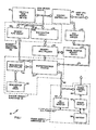
- a data storage system 10 in accordance with the invention includes an MOS volatile main memory 12 coupled by a main memory bus 14 through a memory controller 16 to a host CPU bus 18.
- the host CPU bus 18 is a conventional data processing bus providing connection between the memory controller 16 and a host CPU data processing system.
- the memory controller 16 could be a simple interface circuit arbitrating memory access requests between the host CPU bus 18 and a bus request circuit 20.
- memory controller 16 is configured to appear to the host CPU bus 18 to be a disk drive controller and includes a conventional direct memory access capability as well as conventional circuitry for converting between a cylinder-disk-side-sector disk drive type of address and a corresponding block of random access memory addresses.
- the memory controller 16 accesses the volatile main memoryl2 over the main memory bus 14 to write or read an indicated sequence of data. Because the main memory 12, main memory bus 14, and memory controller 16 are implemented as a disk drive substitute, memory accesses over host CPU bus 18 normally occur for sequences of main memory 12 memory locations corresponding to one or more virtual disk sectors at a time. Consequently, volatile main memory 12 is typically accessed in blocks of sequential memory locations.
- the volatile main memory 12 has a conventional memory address register which can be either loaded with a starting address or simply incremented to the next sequential address under control of an increment signal which is part of the main memory bus 14. Consequently, when reading or writing a sequential block of data for volatile main memory 12, memory controller 16 need merely communicate the first memory address location to the address register of main memory 12. Thereafter, memory controller 16 need only activate the address increment signal on main memory bus 14 for each successive memory word location within main memory 12. Use of the incrementing memory address simplifies data communication between main memory 12 and memory controller 16 by eliminating the need to communicate a 22 bit memory address with every word that is read from or written to main memory 12.
- Main memory 12 is implemented in a maximum configuration of four million words of 80 bits each and is manufactured from conventional dynamic RAM MOS memory chips and includes conventional address decoding, refreshing, and data 10 buffering. Use of the incrementing address register is not an inherent requirement of the present invention but merely a convenience which results from the use of main memory 12 as a fast access disk drive substitute.
- a memory interface subsystem 22 couples to the main memory bus 14 and provides an interface between the volatile main memory 12 and a Z80 based microprocessor system 24 within a shadow memory subsystem 26.
- the memory interface subsystem 22 includes a memory read/write circuit 28 and a bus monitor circuit 30.
- Memory read/write circuit 28 provides a conventional read/write memory interface between microprocessor system 24 and the main memory bus 14 which enables microprocessor system 24 to selectively read and write data at word locations within main memory 12.
- Bus monitor circuit 30 receives as an enable input a LOCAL USE * signal 32 which is derived as a busy signal for memory read/write circuit 28 and enables bus monitor circuit 30 whenever memory read/write circuit 28 is not accessing main memory 12. Bus monitor circuit 30 thus operates to monitor data transfers between the memory controller 16 and main memory 12 over main memory bus 14.
- Bus monitor circuit 30 includes an incrementable address register which duplicates the address register within main memory 12 and is loaded or incremented in sychronism with the address register of main memory 12 so that the bus monitor circuit address register continually reflects the contents of the volatile main memory 12 address register. This duplicate address register would not be required for a traditional main memory 12 which received an address over main memory bus 14 in conjunction with each data access. However, bus monitor circuit 30 must have information as to the address for each write type of data transfer to main memory 12. The duplicate address register provides this information in the special circumstance where sequential memory address locations are indicated by the address register increment signal without a complete memory address being transferred for each data access.
- Each time bus monitor circuit 30 detects a write type of data transfer between memory controller 16 and main memory 12, it writes a logic "1" into a usage monitor memory 40 after gaining access to memory 40 through a memory multiplexer 42.
- Usage monitor memory 40 is a 16K by 1 bit single chip memory which is bit mapped to provide a correspondence between each location within usage monitor memory 40 and a block of word locations within volatile main memory 12. In the present instance, each memory location within usage monitor memory 40 corresponds to a block of 256 80 bit word locations within volatile main memory 12.
- a functional correspondence between addresses of usage monitor memory 40 and addresses of main memory 12 is established by simply selecting the 14 most significant address bits from main memory bus 14 into main memory 12 to address usage monitor memory 40. The 8 least significant bits of the 22 bit address required to access main memory 12 are simply truncated or ignored.
- Bus monitor circuit 30 may thus be an extremely simple circuit which simply responds to the occurrence of a write state on the traditional read/write signal which extends as part of main memory bus 14.
- bus monitor circuit 30 operates to communicate the 14 most significant bits of its duplicate address register as an address input through memory multiplexer 42 to usage monitor memory 40 and writes a single bit logic "1" into the addressed memory location. The consequence of this operation is that each time data is written into a block of memory in main memory 12, a logic 1 is written into a memory location of usage monitor memory 40 which corresponds to that block.
- bus monitor circuit 30 can be implemented in a quite simple manner and need not keep track of whether or not sequential accesses are being made except as required to update the replica address register which is maintained internally of bus monitor circuit 30.
- bus monitor 30 would respond accordingly by writing into the single memory location corresponding thereto in usage monitor memory 256 times in respective sequence.
- Memory multiplexer 42 operates to insure frequent access to usage monitor memory 40 to both the bus monitor circuit 30 and to the shadow memory subsystem 26.
- Memory multiplexer 42 can operate on any conventional basis such as a priority request basis or time division multiplex basis which enables bus monitor circuit 30 to have access to usage monitor memory 40 each time a write access is made to main memory 12 by memory controller 16.
- usage monitor memory 40 is capable of operating twice as fast as main memory 12 so that memory multiplexer 42 merely operates on a conventional time division multiplex basis to make available one cycle of usage monitor memory 40 to both the monitor circuit 30 and shadow memory subsystem 26 during each cycle of main memory 12.
- memory multiplexer 42 allow bus monitor circuit 30 access to usage monitor memory 40 each time a write access is made to a new block of data within main memory 12 and that shadow memory subsystem 26 have frequent access to usage monitor memory 40.
- Power supply subsystem 44 receives standard 60 Hz AC electrical utility power as a main power source 50 which is communicated to an AC power monitor 52, a power supply 54, and to a battery 56 through suitable conventional DC conversion circuitry which continuously recharges or maintains the charge upon battery 56.
- AC power monitor 52 is a conventional power monitor circuit which continuously responds to the input utility power voltage level. If the input power voltage level drops below a selected threshold, AC power monitor circuit 52 provides a signal to microprocessor system 24 and also to a power control circuit 58. AC power monitor circuit 52 similarly indicates a resumption of adequate power after a power failure.
- Microprocessor system 24 responds to a power failure indication by initiating a data preservation and power shutdown mode in response to a power on indication by initiating a data restoration mode of operation.
- Power supply 54 includes the conventional transformer, rectification and filtering circuitry required to produce the DC voltage levels used throughout the data storage system 10. As long as adequate AC utility power is available from main power source 50 power supply 54 utilizes this available power. In the event of a main utility power failure, however, power supply 54 immediately begins extracting power from backup battery 56.
- Power control circuit 58 receives the power from power supply 54 and distributes it to the remainder of the data storage system 10 under control of microprocessor system 24. In a conventional manner, power control circuit 58 switches the power provided to various components in the data storage system 10 as necessary to maintain normal operation. For example, while AC utility power is available all portions of the system are energized. However, while operating on backup power from battery 56, only those portions of the system required for a current operating mode are energized in order to conserve available backup energy. Upon completion of a battery energized data preservation mode following an AC power failure, microprocessor 24 provides to power control circuit 58 a PRESERVATION COMPLETE signal through connector bus 60.
- Power control circuit 58 responds to this PRESERVATION COMPLETE signal by terminating power to all portions of the data storage system 10 except power supply 54, the power control circuit 58 itself, and AC monitor circuit 52. This portion of the circuit consumes very little standby energy and the data storage system 10 is capable of surviving a utility power failure in excess of several days in duration.
- AC power monitor 52 signals power control circuit 58 and microprocessor system 24 over connector bus 60. This signal causes power control circuit 58 to resume distribution of power to all parts of data storage system 10 and initiates a power on reset for microprocessor system 24 which then proceeds to execute a data initialization operation for volatile main memory 12 and then enable normal operation for data storage system 10.
- the shadow memory subsystem 26 includes in addition to the Z80 based microprocessor system 24 a Winchester disk drive controller 62 which couples the microprocessor system 24 to a large, nonvolatile data store which is implemented in the form of a Winchester disk drive 62 in the present example.
- the Winchester disk drive 62 must be capable of storing all of the data in volatile main memory 12 which in the present example is 40 megabytes. If main memory 12 is implemented in a smaller configuration the Winchester disk drive 62 may have a smaller capacity also.
- disk drive 62 is shown as a single drive having a capacity of at least 40 megabytes, it could conventionally be implemented as two 20 megabyte disk drives or any other suitable configuration having adequate storage capacity.
- the microprocessor system 24 includes conventional instruction and scratchpad memory as well as conventional bus drivers, interface circuits and interrupt controllers as necessary to accomplish its system monitoring, data preservation, and data restoration functions.
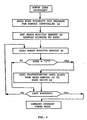
- microprocessor system 24 The operating sequence for microprocessor system 24 is illustrated in Fig. 2.
- a power on reset vector s microprocessor system 24 to a start initialization routine as illustrated in Fig. 2.
- Microprocessor system 24 first issues a command over bus connector 60 to the power supply subsystem 44 to enable full power distribution to all portions of the data storage system 10.
- microprocessor 24 issues a command over a bus connection 70 to bus request circuit 20 to make a high priority bus request to memory controller 16.
- Bus request circuit 20 is a standard bus request interface circuit and is capable of making bus requests of either higher priority than CPU bus 18 or of lower priority as commanded by microprocessor system 24.
- the high priority bus request assures that the microprocessor system 24 and bus request circuit 20 gain control of memory controller 16 immediately if it is not occupied by a request from host CPU bus 18 or if it is so occupied, at the first time that memory controller 16 is relinquished by host CPU bus 18.
- the high priority request locks out any further accesses to memory controller 16 from host CPU bus 18 while the high priority request remains active.
- microprocessor system 24 Upon gaining control of memory controller 16, microprocessor system 24 proceeds to copy the backup image copy of the volatile main memory contents 12 stored in Winchester disk drive 62 from the drive 62 into main memory 12. Although the microprocessor 24 gains control of memory controller 16 to lock out'the host CPU bus 18, the data transfers are made directly over the main memory bus 14 to main memory 12 and bypass the memory controller 16. The transfers are made on a block-by-block basis from Winchester disk drive 68 through Winchester controller 62 to internal RAM microprocessor system 24 and then from the microprocessor system 24 RAM through memory read/write circuit 28 and main memory bus 14 to main memory 12.
- the memory read/write circuit 28 merely provides a conventional interface to the main memory bus 14 to enable microprocessor system 24 to read and write the volatile main memory 12.
- the microprocessor system 24 commands bus request circuit 22 to release the memory controller 16 by terminating the high priority bus request. Normal data transfers between host CPU bus 18 and main memory 12 through memory controller 16 are thus enabled. After releasing memory controller 16 the microprocessor system enters a monitor loop which is illustrated in Fig. 3.
- Microprocessor system 24 maintains an address register for usage monitor memory 40. While different configurations are of course possible, a typical technique for maintaining the usage monitor memory address register would be to utilize a storage location within the internal random access memory of microprocessor system 24. Accesses to usage monitor memory 40 are then made using an indirect addressing mode through this address storage location. In any event, while in the monitor loop the microprocessor system 24 sequentially reads each of the 16K storage locations with usage monitor memory 40 on a repetitive cycle basis. Upon reading each storage location microprocessor tests for the storage of a logic 1 data state. It will be recalled that on alternate cycles of usage monitor memory 40 memory multiplexer 42 grants access to usage monitor memory 40 to the bus monitor circuit 30.
- bus monitor circuit 30 If a write data transfer has occurred between host CP U bus 18 and main memory 12, bus monitor circuit 30 writes a logic 1 data bit into usage monitor memory 40 at the location in usage monitor memory 40 corresponding to the block of addresses in main memory 12 to which the main memory 12 has been written.
- microprocessor system 24 tests the data bit from usage monitor memory 40 for logic 1, if it finds that no logic 1 is stored in the accessed location, this means that no data has been written into the corresponding block of data in the main memory 12. Microprocessor system 24 then proceeds to merely increment the usage monitor memory address and continues reading the next memory location.
- microprocessor 24 finds a logic 1 stored thereat, this means that data has been written into the main memory 12 at some location within the corresponding block of data therein. As a consequence, the backup data image of main memory 12 stored in disk drive 62 no longer matches the data stored in main memory 12 for this block of data.
- Microprocessor system 24 responds to this discrepancy by communicating through bus 70 and bus request circuit 20 a low priority bus request to memory controller 16. This low priority bus request will not interrupt or supersede any bus request to memory controller 16 received over host CPU bus 18. However, as soon as memory controller 16 enters an idle state, the bus request is granted back through bus request circuit 20 to microprocessor system 24.
- microprocessor system 24 Upon gaining control of memory controller 16 microprocessor system 24 then proceeds to read the block of 256 memory locations in volatile main memory 12 corresponding to the last accessed location in usage monitor memory from the main memory 12 into corresponding locations within disk drive 62. Upon updating the data stored by disk drive 62 with the complete block of data, the integrity of the backup image data copy is restored for that block and microprocessor system 24 commands bus request circuit 20 to release the memory controller back to the host CPU bus 16. Microprocessor system 24 then writes a 0 into the currently addressed location within usage monitor memory 40, thus clearing that location and indicating that the backup image data copy stored by disk drive 62 accurately reflects the corresponding block of data in main memory 12.
- the microprocessor system 24 then resumes its process of reading each successive memory location in usage monitor memory 40 looking for the storage of a logic 1 data bit which is an indication that the corresponding block of data stored by volatile main memory 12 has been changed since the image copy thereof was last updated in Winchester disk drive 62.
- the image data copy of main memory 12 data within Winchester disk drive 62 is continually being updated as changes are made in main memory 12 data with any lag between the updating of Winchester disk drive 62 and changing of main memory 12 being reflected by storage of logic 1 indications for corresponding locations in usage monitor memory 40.
- the present invention advantageously provides a direct correlation between five sequential sectors within Winchester disk drive 62 and a block of 256 words within volatile main memory 12. It will be recalled that when the four million word locations within main memory 12 are divided by the 16K storage locations within usage monitor memory 40 the result is 256 which means that a block of 256 word locations within main memory 12 must correspond to each different address within usage monitor memory 40.
- the 80 bit word length for main memory 12 means that there are ten 8 bit bytes for each word and a block of 25 6 word locations thus stores 2560 bytes of information. This matches exactly the storage capacity of five standard sized 512 byte sectors within Winchester disk drive 62. It is thus advantageous to. establish a direct correspondence between five sequential sectors within Winchester disk drive 62 and a block of 256 words within volatile main memory 12.
- AC monitor circuit 52 Upon the occurrence of a power outage, AC monitor circuit 52 generates the LOW POWER signal over bus 60 which is communicated as a high priority interrupt request to microprocessor system 24.
- This interrupt request interrupts microprocessor system 24 immediately and causes it to begin executing a power loss interrupt routine which is illustrated in Fig. 4.
- microprocessor system 24 Upon entering the power loss interrupt routine microprocessor system 24 communicates through connector bus 70 and bus request circuit 20 a high priority bus request to memory controller 16.
- the data transfers over host CPU bus 18 are locked out and microprocessor system 24 sets the address register for usage monitor memory 40 to 0 so that each addressed location within usage monitor memory 40 can be read in sequence exactly once.
- the microprocessor system 24 then enters a loop which is substantially the same as the monitor loop shown in Fig. 3.
- Each sequential address within usage monitor memory 40 is read looking for a logic 1 data bit indicating that the corresponding block of image data in Winchester disk drive 62 does not match the data stored by main memory 12.
- power control circuit 58 terminates power to all of the circuitry of main storage system 10 except those components required to maintain secure data storage and respond to a restoration of main utility power through source 50.
- power need be maintained only to AC power monitor 52 and certain responsive portions of power control circuit 58.
- other portions of the system 10 may require standby power, depending upon specific limitations. For example, were the nonvolatile storage to be provided by a large CMOS memory instead of a Winchester disk drive 62, it might be necessary to provide a small amount of standby power to the CMOS memory.
- a conventional system would require substantially all of the power of battery 56 to provide the backup image of memory 12 data in the nonvolatile memory upon the occurrence of a power failure. Upon restoration of power, it would then take typically 24 hours for battery 56 to be recharged from the utility power supply. If a second or subsequent power failure occurred within this time, the system would shut down but there would be insufficient energy in battery 56 to update the nonvolatile memory with a correct image of the data stored by main memory 12. Important data might thus become lost.
Abstract
Description
- This invention relates to a volatile data store with a backup storage system which is operable during a main power source failure. More particularly the invention relates to a shadow memory system in which a shadow memory is continually updated to reflect changes in data stored by the main memory so that in the event of a power failure only a small portion of the main memory data need be stored using backup power.
- There are many data processing applications in which it is important or essential to preserve data stored in a volatile memory or data store during the course of a main utility power failure. One approach that is sometimes used in critical situations is to provide a short term battery backup and an auxiliary power generator. The battery maintains the integrity of stored data while an engine driving the auxiliary generator is started and brought up to speed. While successful, this arrangement is too costly to be practical for most applications.
- Another commonly used data protection approach is to rely exclusively upon a battery backup in the event of a power failure. In one alternative arrangement the battery backup is used to preserve the integrity of stored data during a power failure. However, large data stores consume large amounts of power and practical limitations on battery backup energy capacity limit data preservation to a few hours. If a power failure lasts more than a few hours critical data will be lost.
- Another known battery backup alternative is to use battery power to "dump" volatile memory data into a nonvolatile memory such as a disk drive upon the occurrence of a power failure. Because of the large amount of energy required to preserve the data for a large memory, practical battery sizes limit preservation of data to one, or at most two, occurrences. Assuming that the backup batteries are rechargeable, it will typically take at least 24 hours to recharge them. However, it is not uncommon for power failures to occur in a rapid sequence of multiple failures and restarts. If more power failures occur than can be accommodated by the data preservation system, data will be lost.
- A data storage system in accordance with the invention includes a volatile main memory coupled to a host CPU through a memory controller and a host CPU bus, a bus monitor circuit, a usage monitor memory, a power supply subsystem with battery backup and a shadow memory subsystem coupled to replicate in nonvolatile storage data stored by the main memory. By continually updating nonvolatile disk storage in the shadow memory subsystem to reflect changes in data stored by the volatile memory, the nonvolatile storage data remains nearly current with the volatile storage data. Upon the occurrence of a main utility power failure only a small portion of the main memory data capacity need be transferred to the nonvolatile store to produce a fully updated copy prior to power shutdown. As a result only a small amount of battery energy is required to complete the data backup in the event of a power failure and several rapid sequence power failures and restarts can be accommodated with practically sized backup batteries.
- The bus monitor circuit is coupled to a main memory bus which provides data communication with the volatile main .. memory. Each time a write access is made to the main memory over the main memory bus, the bus monitor writes into the usage monitor memory an indication of the main memory access.
- A memory multiplexer alternately grants access to the usage monitor memory to the bus monitor circuit and to the shadow memory subsystem in repetitive cycles that occur with sufficient frequency to assure that the bus monitor circuit may access the usage monitor memory each time there is a write access to the main memory.
- The shadow memory subsystem repetitively accesses and sequentially reads the usage monitor memory during the times that it is granted access to the usage monitor memory by a memory multiplexer. As long as the shadow memory subsystem finds no indication of a main memory write, it merely reads the next sequential usage monitor memory location. However, if an indication of a main memory access is found the shadow memory subsystem reads all storage locations in the main memory corresponding to the indication into its nonvolatile storage, clears the indication, and then resumes sequentially reading the usage monitor memory.
- Upon detection of an impending power failure by an AC power monitor within the power supply subsystem, the power supply subsystem indicates the power failure to the shadow memory subsystem and switches from main utility power to battery backup power. The shadow memory subsystem responds to the power failure indication by entering a power shutdown mode in which further data transfers between main memory and the host CPU are inhibited and the usage monitor memory is sequentially read in its entirety with the nonvolatile memory being updated to reflect the data stored at all main memory locations for which an indication of a main memory write access is found. The shadow memory subsystem then commands the power supply subsystem to enter a power down state in which battery power is used only sparingly to monitor the AC power lines.
- In the event that main utility power is restored, the main memory is reinitialized with data from the nonvolatile store and data transfers between the main memory and the host CPU are again enabled. Because the nonvolatile data store was continually updated prior to the power failure, only a relatively small portion of the total main memory data was transferred to nonvolatile storage using battery backup power. Consequently, upon reinitialization of the memory system, the backup batteries still have sufficient energy capacity to accommodate several more rapid succession power failures.
- A better understanding of the invention may be had from a consideration of the following detailed description, taken in conjunction with the accompanying drawings in which:
- Fig. 1 is a block diagram representation of a data storage system with shadow memory backup in accordance with the invention;
- Fig. 2 is a flow chart representation of an initialization routine;
- Fig. 3 is a flow chart representation of a monitor loop routine; and
- Fig. 4 is a flow chart representation of a power loss interrupt routine.
- Referring now to Fig. 1, a
data storage system 10 in accordance with the invention includes an MOS volatilemain memory 12 coupled by a main memory bus 14 through amemory controller 16 to a host CPU bus 18. The host CPU bus 18 is a conventional data processing bus providing connection between thememory controller 16 and a host CPU data processing system. In general, thememory controller 16 could be a simple interface circuit arbitrating memory access requests between the host CPU bus 18 and a bus request circuit 20. - However, in the present
example memory controller 16 is configured to appear to the host CPU bus 18 to be a disk drive controller and includes a conventional direct memory access capability as well as conventional circuitry for converting between a cylinder-disk-side-sector disk drive type of address and a corresponding block of random access memory addresses. In response to read or write commands received over the host CPU bus 18, thememory controller 16 accesses the volatile main memoryl2 over the main memory bus 14 to write or read an indicated sequence of data. Because themain memory 12, main memory bus 14, andmemory controller 16 are implemented as a disk drive substitute, memory accesses over host CPU bus 18 normally occur for sequences ofmain memory 12 memory locations corresponding to one or more virtual disk sectors at a time. Consequently, volatilemain memory 12 is typically accessed in blocks of sequential memory locations. To take advantage of the sequential block accessing and improved system performance, the volatilemain memory 12 has a conventional memory address register which can be either loaded with a starting address or simply incremented to the next sequential address under control of an increment signal which is part of the main memory bus 14. Consequently, when reading or writing a sequential block of data for volatilemain memory 12,memory controller 16 need merely communicate the first memory address location to the address register ofmain memory 12. Thereafter,memory controller 16 need only activate the address increment signal on main memory bus 14 for each successive memory word location withinmain memory 12. Use of the incrementing memory address simplifies data communication betweenmain memory 12 andmemory controller 16 by eliminating the need to communicate a 22 bit memory address with every word that is read from or written tomain memory 12. -
Main memory 12 is implemented in a maximum configuration of four million words of 80 bits each and is manufactured from conventional dynamic RAM MOS memory chips and includes conventional address decoding, refreshing, anddata 10 buffering. Use of the incrementing address register is not an inherent requirement of the present invention but merely a convenience which results from the use ofmain memory 12 as a fast access disk drive substitute. - A
memory interface subsystem 22 couples to the main memory bus 14 and provides an interface between the volatilemain memory 12 and a Z80 basedmicroprocessor system 24 within a shadow memory subsystem 26. - The
memory interface subsystem 22 includes a memory read/write circuit 28 and abus monitor circuit 30. Memory read/write circuit 28 provides a conventional read/write memory interface betweenmicroprocessor system 24 and the main memory bus 14 which enablesmicroprocessor system 24 to selectively read and write data at word locations withinmain memory 12. -
Bus monitor circuit 30 receives as an enable input a LOCAL USE* signal 32 which is derived as a busy signal for memory read/write circuit 28 and enablesbus monitor circuit 30 whenever memory read/write circuit 28 is not accessingmain memory 12.Bus monitor circuit 30 thus operates to monitor data transfers between thememory controller 16 andmain memory 12 over main memory bus 14.Bus monitor circuit 30 includes an incrementable address register which duplicates the address register withinmain memory 12 and is loaded or incremented in sychronism with the address register ofmain memory 12 so that the bus monitor circuit address register continually reflects the contents of the volatilemain memory 12 address register. This duplicate address register would not be required for a traditionalmain memory 12 which received an address over main memory bus 14 in conjunction with each data access. However,bus monitor circuit 30 must have information as to the address for each write type of data transfer tomain memory 12. The duplicate address register provides this information in the special circumstance where sequential memory address locations are indicated by the address register increment signal without a complete memory address being transferred for each data access. - Each time
bus monitor circuit 30 detects a write type of data transfer betweenmemory controller 16 andmain memory 12, it writes a logic "1" into ausage monitor memory 40 after gaining access tomemory 40 through amemory multiplexer 42. -
Usage monitor memory 40 is a 16K by 1 bit single chip memory which is bit mapped to provide a correspondence between each location withinusage monitor memory 40 and a block of word locations within volatilemain memory 12. In the present instance, each memory location withinusage monitor memory 40 corresponds to a block of 256 80 bit word locations within volatilemain memory 12. A functional correspondence between addresses ofusage monitor memory 40 and addresses ofmain memory 12 is established by simply selecting the 14 most significant address bits from main memory bus 14 intomain memory 12 to addressusage monitor memory 40. The 8 least significant bits of the 22 bit address required to accessmain memory 12 are simply truncated or ignored.Bus monitor circuit 30 may thus be an extremely simple circuit which simply responds to the occurrence of a write state on the traditional read/write signal which extends as part of main memory bus 14. Each time a write state occurs on this read/write signal,bus monitor circuit 30 operates to communicate the 14 most significant bits of its duplicate address register as an address input throughmemory multiplexer 42 to usage monitormemory 40 and writes a single bit logic "1" into the addressed memory location. The consequence of this operation is that each time data is written into a block of memory inmain memory 12, alogic 1 is written into a memory location ofusage monitor memory 40 which corresponds to that block. - In a typical memory access procedure,
memory controller 16 would receive a request over host CPU bus 18 which would involve sequentially writing data into each word location within a block or even into all of the word locations within several sequential blocks withinmain memory 12. However,bus monitor circuit 30 can be implemented in a quite simple manner and need not keep track of whether or not sequential accesses are being made except as required to update the replica address register which is maintained internally ofbus monitor circuit 30. Thus, in the event that all 256 word locations within a block of memory withinmain memory 12 are written sequentially, bus monitor 30 would respond accordingly by writing into the single memory location corresponding thereto in usage monitor memory 256 times in respective sequence. -
Memory multiplexer 42 operates to insure frequent access to usage monitormemory 40 to both thebus monitor circuit 30 and to the shadow memory subsystem 26.Memory multiplexer 42 can operate on any conventional basis such as a priority request basis or time division multiplex basis which enablesbus monitor circuit 30 to have access to usage monitormemory 40 each time a write access is made tomain memory 12 bymemory controller 16. In the present instanceusage monitor memory 40 is capable of operating twice as fast asmain memory 12 so thatmemory multiplexer 42 merely operates on a conventional time division multiplex basis to make available one cycle ofusage monitor memory 40 to both themonitor circuit 30 and shadow memory subsystem 26 during each cycle ofmain memory 12. In any event, it is sufficient thatmemory multiplexer 42 allowbus monitor circuit 30 access to usage monitormemory 40 each time a write access is made to a new block of data withinmain memory 12 and that shadow memory subsystem 26 have frequent access to usage monitormemory 40. The more restricted the access of shadow memory subsystem 26 to usage monitormemory 40 the less efficient will be the emergency power saving features of thedata storage system 10. - Before describing the shadow memory subsystem 26 in greater detail it will be helpful to understand the operation of
power supply subsystem 44.Power supply subsystem 44 receives standard 60 Hz AC electrical utility power as amain power source 50 which is communicated to anAC power monitor 52, apower supply 54, and to abattery 56 through suitable conventional DC conversion circuitry which continuously recharges or maintains the charge uponbattery 56. AC power monitor 52 is a conventional power monitor circuit which continuously responds to the input utility power voltage level. If the input power voltage level drops below a selected threshold, ACpower monitor circuit 52 provides a signal tomicroprocessor system 24 and also to a power control circuit 58. ACpower monitor circuit 52 similarly indicates a resumption of adequate power after a power failure.Microprocessor system 24 responds to a power failure indication by initiating a data preservation and power shutdown mode in response to a power on indication by initiating a data restoration mode of operation. -
Power supply 54 includes the conventional transformer, rectification and filtering circuitry required to produce the DC voltage levels used throughout thedata storage system 10. As long as adequate AC utility power is available frommain power source 50power supply 54 utilizes this available power. In the event of a main utility power failure, however,power supply 54 immediately begins extracting power frombackup battery 56. - Power control circuit 58 receives the power from
power supply 54 and distributes it to the remainder of thedata storage system 10 under control ofmicroprocessor system 24. In a conventional manner, power control circuit 58 switches the power provided to various components in thedata storage system 10 as necessary to maintain normal operation. For example, while AC utility power is available all portions of the system are energized. However, while operating on backup power frombattery 56, only those portions of the system required for a current operating mode are energized in order to conserve available backup energy. Upon completion of a battery energized data preservation mode following an AC power failure,microprocessor 24 provides to power control circuit 58 a PRESERVATION COMPLETE signal throughconnector bus 60. Power control circuit 58 responds to this PRESERVATION COMPLETE signal by terminating power to all portions of thedata storage system 10 exceptpower supply 54, the power control circuit 58 itself, and AC monitorcircuit 52. This portion of the circuit consumes very little standby energy and thedata storage system 10 is capable of surviving a utility power failure in excess of several days in duration. Upon resumption of utility power throughmain power source 50, AC power monitor 52 signals power control circuit 58 andmicroprocessor system 24 overconnector bus 60. This signal causes power control circuit 58 to resume distribution of power to all parts ofdata storage system 10 and initiates a power on reset formicroprocessor system 24 which then proceeds to execute a data initialization operation for volatilemain memory 12 and then enable normal operation fordata storage system 10. - The shadow memory subsystem 26 includes in addition to the Z80 based microprocessor system 24 a Winchester
disk drive controller 62 which couples themicroprocessor system 24 to a large, nonvolatile data store which is implemented in the form of aWinchester disk drive 62 in the present example. TheWinchester disk drive 62 must be capable of storing all of the data in volatilemain memory 12 which in the present example is 40 megabytes. Ifmain memory 12 is implemented in a smaller configuration theWinchester disk drive 62 may have a smaller capacity also. In addition, whiledisk drive 62 is shown as a single drive having a capacity of at least 40 megabytes, it could conventionally be implemented as two 20 megabyte disk drives or any other suitable configuration having adequate storage capacity. Although not explicitly shown, themicroprocessor system 24 includes conventional instruction and scratchpad memory as well as conventional bus drivers, interface circuits and interrupt controllers as necessary to accomplish its system monitoring, data preservation, and data restoration functions. - The operating sequence for
microprocessor system 24 is illustrated in Fig. 2. At startup, whether as a result of power turnon or restoration of main utility power, a power on resetvectors microprocessor system 24 to a start initialization routine as illustrated in Fig. 2.Microprocessor system 24 first issues a command overbus connector 60 to thepower supply subsystem 44 to enable full power distribution to all portions of thedata storage system 10. Next,microprocessor 24 issues a command over a bus connection 70 to bus request circuit 20 to make a high priority bus request tomemory controller 16. - Bus request circuit 20 is a standard bus request interface circuit and is capable of making bus requests of either higher priority than CPU bus 18 or of lower priority as commanded by
microprocessor system 24. The high priority bus request assures that themicroprocessor system 24 and bus request circuit 20 gain control ofmemory controller 16 immediately if it is not occupied by a request from host CPU bus 18 or if it is so occupied, at the first time thatmemory controller 16 is relinquished by host CPU bus 18. The high priority request locks out any further accesses tomemory controller 16 from host CPU bus 18 while the high priority request remains active. - Upon gaining control of
memory controller 16,microprocessor system 24 proceeds to copy the backup image copy of the volatilemain memory contents 12 stored inWinchester disk drive 62 from thedrive 62 intomain memory 12. Although themicroprocessor 24 gains control ofmemory controller 16 to lock out'the host CPU bus 18, the data transfers are made directly over the main memory bus 14 tomain memory 12 and bypass thememory controller 16. The transfers are made on a block-by-block basis from Winchester disk drive 68 throughWinchester controller 62 to internalRAM microprocessor system 24 and then from themicroprocessor system 24 RAM through memory read/write circuit 28 and main memory bus 14 tomain memory 12. The memory read/write circuit 28 merely provides a conventional interface to the main memory bus 14 to enablemicroprocessor system 24 to read and write the volatilemain memory 12. When the complete backup memory data image has been transferred fromWinchester disk drive 62 tomain memory 12, themicroprocessor system 24 commandsbus request circuit 22 to release thememory controller 16 by terminating the high priority bus request. Normal data transfers between host CPU bus 18 andmain memory 12 throughmemory controller 16 are thus enabled. After releasingmemory controller 16 the microprocessor system enters a monitor loop which is illustrated in Fig. 3. -
Microprocessor system 24 maintains an address register forusage monitor memory 40. While different configurations are of course possible, a typical technique for maintaining the usage monitor memory address register would be to utilize a storage location within the internal random access memory ofmicroprocessor system 24. Accesses to usage monitormemory 40 are then made using an indirect addressing mode through this address storage location. In any event, while in the monitor loop themicroprocessor system 24 sequentially reads each of the 16K storage locations withusage monitor memory 40 on a repetitive cycle basis. Upon reading each storage location microprocessor tests for the storage of alogic 1 data state. It will be recalled that on alternate cycles ofusage monitor memory 40memory multiplexer 42 grants access to usage monitormemory 40 to thebus monitor circuit 30. If a write data transfer has occurred between host CPU bus 18 andmain memory 12,bus monitor circuit 30 writes alogic 1 data bit intousage monitor memory 40 at the location inusage monitor memory 40 corresponding to the block of addresses inmain memory 12 to which themain memory 12 has been written. - Thus, when
microprocessor system 24 tests the data bit fromusage monitor memory 40 forlogic 1, if it finds that nologic 1 is stored in the accessed location, this means that no data has been written into the corresponding block of data in themain memory 12.Microprocessor system 24 then proceeds to merely increment the usage monitor memory address and continues reading the next memory location. - However, if upon accessing a
usage monitor memory 40 storage location, themicroprocessor 24 finds alogic 1 stored thereat, this means that data has been written into themain memory 12 at some location within the corresponding block of data therein. As a consequence, the backup data image ofmain memory 12 stored indisk drive 62 no longer matches the data stored inmain memory 12 for this block of data.Microprocessor system 24 responds to this discrepancy by communicating through bus 70 and bus request circuit 20 a low priority bus request tomemory controller 16. This low priority bus request will not interrupt or supersede any bus request tomemory controller 16 received over host CPU bus 18. However, as soon asmemory controller 16 enters an idle state, the bus request is granted back through bus request circuit 20 tomicroprocessor system 24. - Upon gaining control of
memory controller 16microprocessor system 24 then proceeds to read the block of 256 memory locations in volatilemain memory 12 corresponding to the last accessed location in usage monitor memory from themain memory 12 into corresponding locations withindisk drive 62. Upon updating the data stored bydisk drive 62 with the complete block of data, the integrity of the backup image data copy is restored for that block andmicroprocessor system 24 commands bus request circuit 20 to release the memory controller back to thehost CPU bus 16.Microprocessor system 24 then writes a 0 into the currently addressed location withinusage monitor memory 40, thus clearing that location and indicating that the backup image data copy stored bydisk drive 62 accurately reflects the corresponding block of data inmain memory 12. Themicroprocessor system 24 then resumes its process of reading each successive memory location inusage monitor memory 40 looking for the storage of alogic 1 data bit which is an indication that the corresponding block of data stored by volatilemain memory 12 has been changed since the image copy thereof was last updated inWinchester disk drive 62. - Under normal circumstances, this process continues indefinitely. As a 256 word block of data is changed in
main memory 12 thebus monitor circuit 30 writes alogic 1 into the corresponding data storage location inusage monitor memory 40 as an indication of the change. Concurrently, and on alternate half cycles,microprocessor subsystem 24 reads sequential address locations inusage monitor memory 40 looking for the stored l's. Each time it finds one it updates the corresponding block of image data inWinchester disk drive 62 and clears thelogic 1 data bit fromusage monitor memory 40. As a consequence, the image data copy ofmain memory 12 data withinWinchester disk drive 62 is continually being updated as changes are made inmain memory 12 data with any lag between the updating ofWinchester disk drive 62 and changing ofmain memory 12 being reflected by storage oflogic 1 indications for corresponding locations inusage monitor memory 40. - Experimental test data suggests that at any point in time it is unlikely that there will be more than four or five blocks of data which have been changed in volatile
main memory 12 without the image thereof being updated inWinchester disk drive 62. As a consequence, upon the occurrence of a main utility power failure, themicroprocessor system 24 need only transfer these four or five blocks of data frommain memory 12 toWinchester disk drive 62 in order to assure that the image data copy stored byWinchester disk drive 62 exactly matches the data stored bymain memory 12 prior to a power shutdown pending the duration of the utility power failure. - While any correspondence between the memory locations within volatile
main memory 12 and storage locations withWinchester disk drive 62 can be utilized, the present invention advantageously provides a direct correlation between five sequential sectors withinWinchester disk drive 62 and a block of 256 words within volatilemain memory 12. It will be recalled that when the four million word locations withinmain memory 12 are divided by the 16K storage locations withinusage monitor memory 40 the result is 256 which means that a block of 256 word locations withinmain memory 12 must correspond to each different address withinusage monitor memory 40. The 80 bit word length formain memory 12 means that there are ten 8 bit bytes for each word and a block of 256 word locations thus stores 2560 bytes of information. This matches exactly the storage capacity of five standard sized 512 byte sectors withinWinchester disk drive 62. It is thus advantageous to. establish a direct correspondence between five sequential sectors withinWinchester disk drive 62 and a block of 256 words within volatilemain memory 12. - Upon the occurrence of a power outage,
AC monitor circuit 52 generates the LOW POWER signal overbus 60 which is communicated as a high priority interrupt request tomicroprocessor system 24. This interrupt request interruptsmicroprocessor system 24 immediately and causes it to begin executing a power loss interrupt routine which is illustrated in Fig. 4. Upon entering the power loss interruptroutine microprocessor system 24 communicates through connector bus 70 and bus request circuit 20 a high priority bus request tomemory controller 16. Upon gaining access tomemory controller 16 the data transfers over host CPU bus 18 are locked out andmicroprocessor system 24 sets the address register forusage monitor memory 40 to 0 so that each addressed location withinusage monitor memory 40 can be read in sequence exactly once. Themicroprocessor system 24 then enters a loop which is substantially the same as the monitor loop shown in Fig. 3. Each sequential address withinusage monitor memory 40 is read looking for alogic 1 data bit indicating that the corresponding block of image data inWinchester disk drive 62 does not match the data stored bymain memory 12. - As soon as a
logic 1 is found, the corresponding image block indisk drive 62 is updated and a 0 is written intousage monitor memory 40. After all of the storage locations withinusage monitor memory 40 have been read, as indicated by encountering the highest address of 16K-1, the power loss interrupt exits the monitor preservation loop and issues a command overbus 60 forpower supply subsystem 44 to enter a standby power mode. In this mode power control circuit 58 terminates power to all of the circuitry ofmain storage system 10 except those components required to maintain secure data storage and respond to a restoration of main utility power throughsource 50. In the present example, power need be maintained only toAC power monitor 52 and certain responsive portions of power control circuit 58. In general, other portions of thesystem 10 may require standby power, depending upon specific limitations. For example, were the nonvolatile storage to be provided by a large CMOS memory instead of aWinchester disk drive 62, it might be necessary to provide a small amount of standby power to the CMOS memory. - In any event, because only a few blocks of data need be written into the nonvolatile memory upon the occurrence of a power failure, only a few seconds worth of battery power are consumed instead of the 15 to 20 minutes that might be typically required to completely copy all of the four million words of data from volatile
main memory 12 into thedisk drive 62 or other nonvolatile storage. As a consequence, 10 to 20 or more rapid sequence power failures could occur and be fully accommodated by thedata storage system 10. - In contrast, a conventional system would require substantially all of the power of
battery 56 to provide the backup image ofmemory 12 data in the nonvolatile memory upon the occurrence of a power failure. Upon restoration of power, it would then take typically 24 hours forbattery 56 to be recharged from the utility power supply. If a second or subsequent power failure occurred within this time, the system would shut down but there would be insufficient energy inbattery 56 to update the nonvolatile memory with a correct image of the data stored bymain memory 12. Important data might thus become lost. - While there has been shown and described above a data storage system with a shadow memory subsystem maintaining the integrity of stored data throughout multiple rapid sequential power failures for the purpose of enabling a person of ordinary skill in the art to make and use the invention, it will be appreciated that the invention is not limited thereto. Accordingly, any modifications, variations, or equivalent arrangements within the scope of the attached claims should be considered to be within the scope of the invention.
Claims (23)
Applications Claiming Priority (2)
| Application Number | Priority Date | Filing Date | Title |
|---|---|---|---|
| US62841784A | 1984-07-06 | 1984-07-06 | |
| US628417 | 1984-07-06 |
Publications (2)
| Publication Number | Publication Date |
|---|---|
| EP0167322A2 true EP0167322A2 (en) | 1986-01-08 |
| EP0167322A3 EP0167322A3 (en) | 1988-06-15 |
Family
ID=24518791
Family Applications (1)
| Application Number | Title | Priority Date | Filing Date |
|---|---|---|---|
| EP85304350A Withdrawn EP0167322A3 (en) | 1984-07-06 | 1985-06-18 | Shadow memory system |
Country Status (3)
| Country | Link |
|---|---|
| EP (1) | EP0167322A3 (en) |
| JP (1) | JPS6126155A (en) |
| CA (1) | CA1228929A (en) |
Cited By (8)
| Publication number | Priority date | Publication date | Assignee | Title |
|---|---|---|---|---|
| EP0418448A1 (en) * | 1989-09-22 | 1991-03-27 | Computers Iberica S.A. | A system for the protection against mains supply failure for computers by storing the processed information held in the volatile memory |
| EP0460308A1 (en) * | 1989-01-23 | 1991-12-11 | Honeywell Inc. | Methods for control data base updating of a redundant processor in a process control system |
| EP0460307A1 (en) * | 1989-01-23 | 1991-12-11 | Honeywell Inc. | Apparatus for tracking predetermined data for updating a secondary data base |
| AU638011B2 (en) * | 1990-05-18 | 1993-06-17 | Honeywell Inc. | Apparatus for tracking predetermined data for updating a secondary data base |
| GB2263024A (en) * | 1991-12-31 | 1993-07-07 | Lopez Jose Antonio Gutierrez | Safety device for computers with uninterrupted power feed |
| US6625705B2 (en) * | 1993-04-23 | 2003-09-23 | Emc Corporation | Remote data mirroring system having a service processor |
| EP1548546A2 (en) * | 2003-12-23 | 2005-06-29 | Samsung Electronics Co., Ltd. | Method and circuit for preservation of user data in a mobile terminal |
| US20130007478A1 (en) * | 2011-06-30 | 2013-01-03 | Hon Hai Precision Industry Co., Ltd. | Testing system for backup battery module of storing system |
Families Citing this family (6)
| Publication number | Priority date | Publication date | Assignee | Title |
|---|---|---|---|---|
| JPS6359644A (en) * | 1986-08-29 | 1988-03-15 | Fujitsu Ltd | Semiconductor filing device |
| JPS6371752A (en) * | 1986-09-12 | 1988-04-01 | Fujitsu Ltd | Semiconductor filing device |
| US7707387B2 (en) | 2005-06-01 | 2010-04-27 | Microsoft Corporation | Conditional execution via content addressable memory and parallel computing execution model |
| US7451297B2 (en) | 2005-06-01 | 2008-11-11 | Microsoft Corporation | Computing system and method that determines current configuration dependent on operand input from another configuration |
| US7793040B2 (en) | 2005-06-01 | 2010-09-07 | Microsoft Corporation | Content addressable memory architecture |
| JP5974620B2 (en) | 2012-05-10 | 2016-08-23 | 富士通株式会社 | Backup method, program, and backup device |
Citations (3)
| Publication number | Priority date | Publication date | Assignee | Title |
|---|---|---|---|---|
| JPS5856165A (en) * | 1981-09-30 | 1983-04-02 | Toshiba Corp | Record update system |
| JPS58103052A (en) * | 1981-12-16 | 1983-06-18 | Toshiba Corp | Automatic data gathering system |
| JPS58200358A (en) * | 1982-05-18 | 1983-11-21 | Mitsubishi Electric Corp | File reprocessing and recovering method on disk base |
Family Cites Families (2)
| Publication number | Priority date | Publication date | Assignee | Title |
|---|---|---|---|---|
| JPS607818B2 (en) * | 1980-04-28 | 1985-02-27 | 横河電機株式会社 | How to back up files |
| JPS59227094A (en) * | 1983-06-06 | 1984-12-20 | Toshiba Corp | Electronic computer |
-
1985
- 1985-05-23 JP JP11129085A patent/JPS6126155A/en active Pending
- 1985-06-18 EP EP85304350A patent/EP0167322A3/en not_active Withdrawn
- 1985-06-26 CA CA000485364A patent/CA1228929A/en not_active Expired
Patent Citations (3)
| Publication number | Priority date | Publication date | Assignee | Title |
|---|---|---|---|---|
| JPS5856165A (en) * | 1981-09-30 | 1983-04-02 | Toshiba Corp | Record update system |
| JPS58103052A (en) * | 1981-12-16 | 1983-06-18 | Toshiba Corp | Automatic data gathering system |
| JPS58200358A (en) * | 1982-05-18 | 1983-11-21 | Mitsubishi Electric Corp | File reprocessing and recovering method on disk base |
Non-Patent Citations (5)
| Title |
|---|
| DIGITAL DESIGN, October 1983, pages 92-97, "Solid state disks optimize throughput" * |
| IBM TECHNICAL DISCLOSURE BULLETIN, vol. 17, no. 5, October 1974, pages 1449-1450, New York, US; R.O. HIPPERT et al.: "Saving random-access memory in the event of a power failure" * |
| PATENT ABSTRACTS OF JAPAN, vol. 7, no. 142 (P-205)[1287], 22nd June 1983; & JP-A-58 056 165 (TOKYO SHIBAURA DENKI K.K.) 2nd April 1983 * |
| PATENT ABSTRACTS OF JAPAN, vol. 7, no. 210 (P-223)[1355], 16th September 1983; & JP-A-58 103 052 (TOKYO SHIBAURA DENKI K.K.) 18-06-1983 * |
| PATENT ABSTRACTS OF JAPAN, vol. 8, no. 51 (P-259)[1488], 8th March 1984; & JP-A-58 200 358 (MITSUBISHI DENKI K.K.) 21-11-1983 * |
Cited By (10)
| Publication number | Priority date | Publication date | Assignee | Title |
|---|---|---|---|---|
| EP0460308A1 (en) * | 1989-01-23 | 1991-12-11 | Honeywell Inc. | Methods for control data base updating of a redundant processor in a process control system |
| EP0460307A1 (en) * | 1989-01-23 | 1991-12-11 | Honeywell Inc. | Apparatus for tracking predetermined data for updating a secondary data base |
| AU637611B2 (en) * | 1989-01-23 | 1993-06-03 | Honeywell Inc. | Method for control data base updating of a redundant processor in a process control system |
| EP0418448A1 (en) * | 1989-09-22 | 1991-03-27 | Computers Iberica S.A. | A system for the protection against mains supply failure for computers by storing the processed information held in the volatile memory |
| AU638011B2 (en) * | 1990-05-18 | 1993-06-17 | Honeywell Inc. | Apparatus for tracking predetermined data for updating a secondary data base |
| GB2263024A (en) * | 1991-12-31 | 1993-07-07 | Lopez Jose Antonio Gutierrez | Safety device for computers with uninterrupted power feed |
| US6625705B2 (en) * | 1993-04-23 | 2003-09-23 | Emc Corporation | Remote data mirroring system having a service processor |
| EP1548546A2 (en) * | 2003-12-23 | 2005-06-29 | Samsung Electronics Co., Ltd. | Method and circuit for preservation of user data in a mobile terminal |
| EP1548546A3 (en) * | 2003-12-23 | 2006-08-30 | Samsung Electronics Co., Ltd. | Method and circuit for preservation of user data in a mobile terminal |
| US20130007478A1 (en) * | 2011-06-30 | 2013-01-03 | Hon Hai Precision Industry Co., Ltd. | Testing system for backup battery module of storing system |
Also Published As
| Publication number | Publication date |
|---|---|
| JPS6126155A (en) | 1986-02-05 |
| EP0167322A3 (en) | 1988-06-15 |
| CA1228929A (en) | 1987-11-03 |
Similar Documents
| Publication | Publication Date | Title |
|---|---|---|
| US4959774A (en) | Shadow memory system for storing variable backup blocks in consecutive time periods | |
| US5414861A (en) | Data protection system using different levels of reserve power to maintain data in volatile memories for any period of time | |
| US5799200A (en) | Power failure responsive apparatus and method having a shadow dram, a flash ROM, an auxiliary battery, and a controller | |
| US6336161B1 (en) | Computer configuration system and method with state and restoration from non-volatile semiconductor memory | |
| EP0167322A2 (en) | Shadow memory system | |
| US4763333A (en) | Work-saving system for preventing loss in a computer due to power interruption | |
| US4506323A (en) | Cache/disk file status indicator with data protection feature | |
| US5163153A (en) | Low-power, standby mode computer | |
| US5241680A (en) | Low-power, standby mode computer | |
| US5937433A (en) | Method of controlling hard disk cache to reduce power consumption of hard disk drive used in battery powered computer | |
| US6336174B1 (en) | Hardware assisted memory backup system and method | |
| US5109505A (en) | Semiconductor memory disk apparatus with backup device capable of being accessed immediately after power source is recovered | |
| US20010001879A1 (en) | Method and apparatus for saving device state while a computer system is in sleep mode | |
| EP0778526A1 (en) | Magnetic disk controller for backing up cache memory | |
| US7058835B1 (en) | System, method and apparatus for controlling supply of backup power to first and second power planes in the event of a power failure of a main power supply | |
| EP1351146A1 (en) | Power management system and method with recovery after power failure | |
| US5524203A (en) | Disk cache data maintenance system | |
| EP0826218B1 (en) | A modular cache memory battery backup system | |
| US6154846A (en) | System for controlling a power saving mode in a computer system | |
| US7024571B1 (en) | Conversion card and method to convert a general purpose personal computer into a dedicated mass storage appliance | |
| US6851012B2 (en) | Information processing system, information processing method and readable-by-computer recording medium | |
| US5424994A (en) | Semiconductor memory unit used as external storage | |
| JPH03233743A (en) | Storage controller and storage device | |
| EP0487910A1 (en) | Portable computer for varying read/write cycle according to type of memory card | |
| JPH064228A (en) | Semiconductor disk device |
Legal Events
| Date | Code | Title | Description |
|---|---|---|---|
| PUAI | Public reference made under article 153(3) epc to a published international application that has entered the european phase |
Free format text: ORIGINAL CODE: 0009012 |
|
| AK | Designated contracting states |
Designated state(s): DE FR GB IT NL SE |
|
| PUAL | Search report despatched |
Free format text: ORIGINAL CODE: 0009013 |
|
| AK | Designated contracting states |
Kind code of ref document: A3 Designated state(s): DE FR GB IT NL SE |
|
| 17P | Request for examination filed |
Effective date: 19881025 |
|
| 17Q | First examination report despatched |
Effective date: 19901105 |
|
| STAA | Information on the status of an ep patent application or granted ep patent |
Free format text: STATUS: THE APPLICATION HAS BEEN WITHDRAWN |
|
| 18W | Application withdrawn |
Withdrawal date: 19910429 |
|
| R18W | Application withdrawn (corrected) |
Effective date: 19910429 |
|
| RIN1 | Information on inventor provided before grant (corrected) |
Inventor name: DAVIS, JOHN E. |