EP0165058A2 - Communication systems with portable units - Google Patents
Communication systems with portable units Download PDFInfo
- Publication number
- EP0165058A2 EP0165058A2 EP85304179A EP85304179A EP0165058A2 EP 0165058 A2 EP0165058 A2 EP 0165058A2 EP 85304179 A EP85304179 A EP 85304179A EP 85304179 A EP85304179 A EP 85304179A EP 0165058 A2 EP0165058 A2 EP 0165058A2
- Authority
- EP
- European Patent Office
- Prior art keywords
- transmitter
- receiver
- base unit
- portable
- photo
- Prior art date
- Legal status (The legal status is an assumption and is not a legal conclusion. Google has not performed a legal analysis and makes no representation as to the accuracy of the status listed.)
- Withdrawn
Links
- 238000004891 communication Methods 0.000 title claims abstract description 31
- 230000009977 dual effect Effects 0.000 claims description 20
- 238000001514 detection method Methods 0.000 claims description 13
- 230000005855 radiation Effects 0.000 claims description 12
- 230000008878 coupling Effects 0.000 claims description 10
- 238000010168 coupling process Methods 0.000 claims description 10
- 238000005859 coupling reaction Methods 0.000 claims description 10
- 230000035945 sensitivity Effects 0.000 claims description 8
- 230000006870 function Effects 0.000 claims description 7
- 230000000295 complement effect Effects 0.000 claims description 6
- 238000002955 isolation Methods 0.000 claims description 6
- 230000000712 assembly Effects 0.000 claims description 4
- 238000000429 assembly Methods 0.000 claims description 4
- 230000003287 optical effect Effects 0.000 claims description 4
- 238000000926 separation method Methods 0.000 claims description 4
- 230000002708 enhancing effect Effects 0.000 claims 2
- 230000003247 decreasing effect Effects 0.000 claims 1
- 238000005286 illumination Methods 0.000 abstract 1
- 239000003990 capacitor Substances 0.000 description 19
- 230000000694 effects Effects 0.000 description 8
- 230000005540 biological transmission Effects 0.000 description 5
- 238000010586 diagram Methods 0.000 description 5
- 230000001939 inductive effect Effects 0.000 description 5
- 230000005236 sound signal Effects 0.000 description 3
- 238000001914 filtration Methods 0.000 description 2
- 230000003213 activating effect Effects 0.000 description 1
- 230000004075 alteration Effects 0.000 description 1
- 230000000903 blocking effect Effects 0.000 description 1
- 230000001276 controlling effect Effects 0.000 description 1
- 238000007599 discharging Methods 0.000 description 1
- 230000000873 masking effect Effects 0.000 description 1
- 238000000034 method Methods 0.000 description 1
- 230000000116 mitigating effect Effects 0.000 description 1
- 230000010355 oscillation Effects 0.000 description 1
- 238000005086 pumping Methods 0.000 description 1
- 230000001105 regulatory effect Effects 0.000 description 1
- 239000007787 solid Substances 0.000 description 1
- 238000001228 spectrum Methods 0.000 description 1
Images


Classifications
-
- H—ELECTRICITY
- H04—ELECTRIC COMMUNICATION TECHNIQUE
- H04M—TELEPHONIC COMMUNICATION
- H04M1/00—Substation equipment, e.g. for use by subscribers
- H04M1/72—Mobile telephones; Cordless telephones, i.e. devices for establishing wireless links to base stations without route selection
- H04M1/725—Cordless telephones
- H04M1/737—Characterised by transmission of electromagnetic waves other than radio waves, e.g. infrared waves
Definitions
- the present invention relates to portable communication systems, and in awakeularsuch systems intended to provide remote or portable communication through a network such as the telephone line.
- Such communication operate in a full duplex mode permitting simultaneous transmission and reception at the portable unit as is typical of conventional telephone head sets.
- Battery drain in the portable unit limits its useful life between replacement or recharges. Isolation of the light wave transmit and receive signal paths is necessary so as to avoid interference between the paths. Loss of sensitivity results from detuning of system parameters, and audio feedback due to coupling into the two wire telephone network.
- a portable hand held unit can suffer from blockage of the light wave signal by head and hair shadowing during use.
- Battery drain is a significant problem because in order to ensure adequate signal strength over a wide range, the system must be capable of emitting a high level of modulated light. In most situations, the portable unit will be much closer to the network, not requiring such high emission energies and therefore wasting substantial battery power.
- the required level of modulated light at the photo receiver input depends on the maximum acceptable background noise as perceived by the user during conversation pulses.
- both transmit and receive channels are simultaneously operative, and because the receive photo sensors must be sensitive to very low light levels, a substantial potential for interference results from their proximity to the high level emitted radiation from the portable, or network associated transmitting emitters.
- the photo sensors at the receiver must be able to discriminate between the locally emitted channel, at many orders of magnitude greater intensity, and the incoming signal to which they are intended to be solely responsive.
- narrow band pulse rate modulation is typically utilized for the optical transmit and receive links between the portable unit and the network associated receiving and transmitting equipment. Be cause of the narrow bandwidth thus utilised, and potential abuse to which the portable unit may be subjected in dropping or other accidents, slight detune of the equipment can produce an apparent loss in sensitivity and inadequacy of the portable unit in operating at distances.
- a portable light wave full duplex communication system operating in an efficient and highly sensitive manner.
- the system utilises specific techniques to overcome all of the problems identified above and thereby produces and efficient utilisation of battery energy, provides light wave channel isolation, minimises the effects of frequency detuning of the communication system, bidirectionally couples ingoing and outgoing audio signals to the telephone network without the use of inductive balancing elements and provides minimum perceived noise for given light-wave level at the receiver's photo sensor input.
- both a portable and a base unit are provided in communication with each other via infrared light waves.
- the base unit includes a receiver responsive at a first frequency to signals transmitted by a portable unit transmitter with the received signals applied the telephone network through a coupling system with an inductorless balancing network utilising duals of inductive circuits to accomplish the function of conventional inductive couplers.
- the base unit also includes transmitter responsive to signals coupled from the telephone network for light wave transmission at a second frequency to a receiver located within the portable unit.
- Both channels are operated simultaneously, providing duplex operation.
- the frequency ratios are in the square root of two in order to maximize the separation between the channels and all possible harmonics.
- pulse rate modulation is utilized wherein substantially fifty percent duty cycle pulses of well shaped form are utilized in order to minimize the harmonic content in the transmitted radiation.
- assemblies for the photo emitters and photo sensors are utilized which prevent the photo sensors from seeing reflection, in the near field, from the photo emitters associated with each of the portable or base units.
- the photo emitters in the base unit are additionally placed at the bottom of a recess and permitted to radiate in a large solid angle pattern utilizing curved prism optics.
- the two communication channels at the two frequencies are operated in a closed loop which maintains the detected modulated radiation level at the base unit receiving photo sensors at a substantially constant level This level is set to provide fully adequate audio or voice reproduction without requiring unnecessary emission energies when the portable unit is closer or in a more direct transmitting path to the photo sensors in the base unit.
- the closed loop further includes frequency control over the transmitter at the base unit which continuously adjusts its frequency for optimum or maximum sensitivity of the portable unit receiver. This forces the base unit transmitter to track any slight frequency changes in the receiver unit center frequency resulting from mishandling or dropping of the portable unit.
- Each receiver and transmitter include complementary nonlinear sensitivity or gain characteristics which reduce the receiver sensitivity at very low input levels so that the perceived noise during voice pulses is substantially reduced. Gain is restored to a higher level for higher level inputs where the voice or audio input serves to mask the noise.
- Two sets of photo emitters and photo sensors are located on the portable unit - one set at each end of the hand set. With this arrangement blockage of the light wave signal is unlikely.
- the present invention contemplates a portable communication system typically operative with the telephone network and utilising duplex light wave communication links between a portable transmitter receiver pair and base station transmitter-receiver pair typically associated with the telephone network.
- the system is optimized for fidelity of audio reproduction and minimal battery drain, minimal interference between duplex communication channels and provides frequency tracking to compensate for frequency deviations in the portable unit receiving circuitry. Noise insensitivity at low levels is also acheived as well as low susceptibility to light wave blocking.
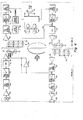
- FIG. 1 A typical unit according to the invention is illustrated in Fig. 1 showing a base unit 10 communicative with the phone lines 12 and cradling a portable or hand set unit 14.
- the base unit includes a recessed assembly 16 containing photo emitters and photo sensors for use with transmission and receiving circuitry within the base unit 10.
- a set of pins 18 provide battery charging power to the portable unit 14 and, respond to the weight of the portable unit 14 to disconnect the system from the telephone network 12 as is conventional in telephone equipment.
- the hand set 14 includes a speaking portion 20 having a microphone and a listening portion 22 having an ear piece or speaker.
- an assembly 24 containing photo emitters and photo sensors associated with the transmission and reception circuitry of the portable unit 14 and covered by a primarily infrared transmissive, and therefore dark red, plastic covering 26.
- the assembly 16 is illustrated in Fig. 2 to contain typically a printed circuit board 30 on which is located a metallic collar 32 recessed within which at the four interior corners of the collar, are photo sensors 34, typically PIN photo diodes.
- the diodes 34 are located deep within the recess provided by the collar 32, but are enabled to see into a broad angle above and about the base unit 10 by prisms 36 cemented over the diodes 34.
- the prisms have partially spherical objective surfaces 38 and reflecting facets 40.
- Also contained within the collar 32 are contacts 42 and pins 44 which contact corresponding contacts 46 within the portable unit 14 for communicating battery charging power thereto.
- the assembly 16 includes, on another portion, an array of photo emitters 48 which are located below the light path from the diodes 34 as shielded partially by the collar 32, but are made to produce infrared modulated radiation through a reflector assembly 50 that reflects light over broad angles from one or more of the light emitting diodes 48.
- the assembly of Fig. 2 thus provides isolation between photo emission and photo sensing functions.
- Fig. 3 illustrates one of the assemblies 24 for the portable unit 14 containing, on each end thereof, an array typically of four light emitters 54.
- a side recess 56 on each side has an interior panel 58 and contains a photo sensor 60.
- the panel 58 prevents the photo sensor 60 from seeing near field radiation from the photo emitters 54 but at the same time permits sensitivity to ambient modulated infrared radiation typically transmitted from the photo emitters 48 in the base unit.
- the assembly of Fig. 3 appears on both ends of the portable unit affording good light wave access for all modes of handling.
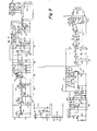
- the portable unit shown to the left in Fig. 4, contains a microphone 64 the output of which is applied to an amplifier 66 for level boosting.
- the output of the amplifier 66 is applied through a filter 68 which provides frequency pre-emphasis that effects a high frequency rolloff for subsequent pulse rate (FM) modulation.
- the output of the pre-emphasis filter 68 is applied to a dual slope gain module having an output level versus input level transfer function as illustrated in the graph associated with the unit.
- the gain is nonlinear, increasing significantly at low levels. This permits the receiver to possess an opposite characteristic so that when masking audio signals are not present, the receiver gain is reduced to avoid the appearance of noise.
- the output of the dual slope gain system 70 is applied to a voltage controlled oscillator 72 which results in a width modulated pulse repetition rate. This output is applied to an LED driver circuit 74 which generates substantially fifty percent duty cycle pulses to a series of light emitting diodes 76. The power level generated by the driver 74 is controlled by a signal taken from the receiver portion of the portable unit 14.
- the receiver in the base unit 10 includes a set of photo sensors 80 responsive to pulse rate and width modulated infrared radiation emitting from the diodes 76.
- the sensed emission is applied through an amplifier/filter 82 to a integrated circuit module 84 acting as a preamplifier, limiter and FM demodulator.
- the filter 82 converts the pulse rate modulated signal to an FM signal.
- the demodulated output from the unit 84 is applied through a dual slope gain circuit 86 having a gain characteristic, nonlinear and complementary to the gain of the dual slope circuit 70 so as to restore a substantially overall linear gain characteristic to the signal provided at its output and reduce low level noise during periods of no modulation.
- This signal is applied through a de-emphasis filter 88 to restore the normal frequency spectrum, prior to being altered by the pre-emphasis filter 68.
- the output of the de-emphasis filter is applied through an active hybrid circuit 90, having impedance dual and impedance balancing circuits 92 and 94 explained below.
- the hybrid coupler 90 applies the received signal to the telephone lines 12 through a simple isolation transformer 96.
- the hybrid circuit 90 also receives from the telephone lines 12, via the transformer 96, incoming network signals and separates them from the outgoing signals for application to a base unit transmitter side pre-emphasis filter 100.
- the output of the pre-emphasis filter 100 is applied through a dual slope gain circuit 102 to a voltage controlled oscillator 104 and in turn an LED IR emitter driver 106.
- the components 100-106 are substantially the same as those found in the transmitter section of the portable unit 14.
- the demodulator 84 has an output, applied through a level detector 85, representing at a DC level the signal strength received through the diodes 80 at the base unit receiver.
- This signal strength will in turn represent the distance between the base unit 10 and the portable unit 14 or other factors affecting the strength of the signal sensed from the emitting portable unit transmitter diodes 76.
- This DC signal level is applied through a high impedance 108 to the input of the voltage controlled oscillator 104, imparting a current summing effect.
- the result of the DC signal applied through the resistor 108 is to shift the center frequency of oscillation of the oscillator 104 for purposes of frequency compensation and portable unit output power control as described below.
- the output of the LED driver 106 in the base unit 10 activates light emitting diodes 110 to emit infrared, pulse rate modulated radiation which is in turn sensed by photo sensors 112 associated with portable unit 14.
- the signal resulting from infrared radiation sensed by the diodes 112 is applied through an amplifier 113 to an integrated circuit 114 comprising, like the integrated circuit 84, a filter, limiter and demodulator for providing FM demodulation of the pulse rate modulated signal detected by diodes 112.
- the output of the demodulator 114 is applied to a dual slope gain circuit 116, having the complementary slope characteristic to the circuit 102 and thereby restoring substantially linear gain characteristics throughout the transmitter receiver channel and reducing low volume noise.
- the output of the dual slope gain circuit is applied to a de-emphasis filter 118 restoring the original frequency components prior to alteration by the filter 100.
- the output of the filter 118 is applied through a driver amplifier 122 to an ear piece 122, typically associated with the hearing position 22 of the portable unit 14.
- the output of the demodulator 114 is also applied through an integrator 124 to the LED driver 74 to control the level of output power and therefore battery drain utilized in activating the infrared diode 76.
- the feedback from the demodulator 114 to the driver 74 in combination with the feedback from the demodulator 84 through level detector 85 to the voltage controlled oscillator 104 effects a closed loop system, the result of which is to maintain control over the output power in the diodes 76 such that the sensed intensity at the photo sensors 80 remains substantially constant.
- this level affects the frequency of the base unit transmitted radiation center frequency which in turn affects the DC level of the demodulator 114 in such manner that the power output is regulated through frequency variations.
- any small frequency deviations in the receiver tune produce an immediate retracking of the frequency of the center band of the oscillator 104. This accommodates any frequency shifting in the center frequency of the demodulator 114 resulting from mishandling of the unit.
- a microphone 130 suitably biased and frequency compensated, has its audio signal applied through an amplifier 132 to a pre-erriphasis circuit 134 having an active FET transistor 136 and feedback capacitor 137 which effect roll off of high frequencies to keep the high frequencies out of the modulator.
- the output of the pre-emphasis network 134 is applied to a dual slope gain amplifier 138 having a set of feedback diodes 140 the effect of which is to reduce the feedback impedance at high levels and thus effect a form of gain reduction complementary to the receivers low level gain reduction and high level gain increase.
- the output of the dual slope circuit 138 is applied to a demodulator circuit 142 containing an integrated circuit 144, typically a Model 555 timer, integrated circuit operating as a voltage controlled oscillator.
- the circuit 144 applies an output on a pin 3 to the gate of an FET 146 which controls a discharge path to ground through sets of infrared emitting diodes 148 and 150 at opposite ends of the portable unit, discharging a previously charged capacitor 147.
- the charge on the capacitor 147 determines the output power as explained below.
- the chip 144 functions essentially to produce a triangle wave which, reverses at the levels defined by pins 2 and 8. With the level on 2 determined by the input signal level from the dual slope circuit 138 such that the higher it is the more rapidly the VCO 144 switches, and more frequently the pulses appear on the line from pin 3.
- the output of the loop integrator 162 controls the power driving circuit which charges the capacitor 147 through inductive current pumping by a transistor 150, latched by a transistor 152, to conduct through an inductor 156. With turnon of the transistor 150, the inductor 156 is current loaded at at turnoff dumps the current through diode 158 into the capacitor 147, thereby charging it up to a high voltage level, significantly greater than the driving battery voltage.
- the values of the biasing potentials for the circuit 144 are adjusted to provide a substantially fifty percent duty cycle output pulse from pin 3 applied to the transistor 146 which controls the timing of the application of current from the capacitor 147 through the diodes 148.
- the capacitor discharge matches the LED turnon to yield a square pulse, low in harmonics.
- the energy stored in the capacitor 147 governs the output power and is under the control of the output of an integrating amplifier 162 which is driven by the output of the receiving side of the portable unit as described below.
- the output of the integrator 162 is applied to pin 7, of the circuit 144 and to the gate of the transistor 150 controlling the level of charge application to the capacitor 147.
- the charge level on the capacitor 147 is fed back to the integrator 162 at a current summing input along with the output from the demodulator in the receiver section. In this manner, a higher input signal from the receiver requires a lower signal from the capacitor 147 and vice versa effecting the power control through the level applied to pin 7.
- Pin 7 provides a separate switching to ground in unison with the pulse output on pin 3. The greater the output of the integrator 162, representing a more strongly received signal, the shorter is the on time of transistor 150 and the less charge is applied to the capacitor 147.
- the networks include active FET transistors 176 and 178 to provide impedance matching and frequency matching characteristics for the photo diodes.
- the output of the transistors 176 and 178 are combined in an amplifier stage 180 having a low noise transistor 182, emitter driven by the outputs of the photo sensor PETS.
- the receiver has a filter section 184 which provides LC tuning to the base unit transmitter frequency.
- the pulse rate modulated signal is converted by means of filtering to an FM signaL
- the collector output from the transistor 182 is applied through a filter 186, having a zero at the transmitter frequency for the local transmitter, in this case the transmitter in the portable unit.
- This filtered signal is applied to an integrated circuit 190 functioning as a preamplifier, limiter, and demodulator.
- the circuit includes a filter 192 which tunes the integrated circuit to a center frequency for the base unit transmitter center frequency.
- the output of the demodulator 190 is applied through a "twin T" filter 194 which filters out frequencies at twice the frequency of the local transmitter and applies it through an amplifier 196 to a dual slope amplifier 198 acting with an inverse characteristic, complementary to the dual slope amplifier 138 to restore substantial circuit linearity and effect quieting when low levels of modulation exist.
- the output of the dual slope circuit 198 drives a bridge audio amplifier 200 through a pair of amplifiers which are connected to opposite sides of an earphone 202.
- the output of the demodulator 190 which represents received signal level, is bypassed through a loop filtering and capacitor 204 and applied to the input of the integrator 162 as the power output control sensed through frequency deviations.
- circuitry exemplary of an implementation of the hybrid circuit 90 illustrated in Fig. 4 and associated duals 92 and 94 are illustrated.
- the transformer 96 applies a signal through a DC bypass capacitor 210 to a noninverting input of an amplifier 212 having input resistances and feedback resistances which determine the gain characteristics.
- the output of the amplifier 212 is applied to the pre-emphasis filter 100 in the base station transmitter circuitry.
- the signal on the high side of the capacitor 210 is also applied through a resistor 214 to the output of an audio amplifier 216 at the output of the receiver side.
- Across the output of the audio amplifier 216 is a parallel combination of a high impedance resistance 218 with an RC series combination 220.
- the noninverting input of the amplifier 212 is fed from this parallel circuit and is in turn shunted by a series RC circuit 222 feeding into ground through a parallel RC circuit 224.
- the combination of the parallel circuit 224 and the resistive component of the series circuit 224 provides the impedance balancing circuitry of Fig. 4 while the combination of the series circuit 220 provides the impedance dual circuit 92 of Fig. 4.
- the level detector circuit 85 is illustrated. As shown there, the output from pin 3 of the integrated circuit 190 in the base unit receiver section is applied through a coupling capacitor 240, through a resistor 242 to the base of a transistor 244. The amplified output of the collector of the transistor 244 is applied through a coupling capacitor 246 and input resistor 248 to the base of a further transistor 250. The collector output of the transistor 250 is applied through a pi filter comprising a series resistor 252 and shunt capacitors 254 and 256 through a high impedance resistance 258, to give a current summing characteristic to the signal applied thereby to the voltage controlled oscillator 104. In particular, this signal is applied to pin 5 in the chip 144 as utilized in the base unit transmitter section.
Abstract
57 An optimized full duplex light wave communication system having a base unit and a portable unit. Two continuously operative channels exist between the base and portable units for two way communication at frequencies selected to minimize interference despite the presence of light within the environment of use at both frequencies. In addition, photo emitters and sensors are specifically configured in an assembly to minimize cross talk between sensors and emitters A closed loop is formed around the two communication channels that it is operative to regulate the intensity of illumination received at the base photo sensors to a constant level that provides quality audio communications and minimizes portable unit battery drain. The closed loop additionally causes base station transmitter frequency tracking of any center frequency variation in the portable unit receiver.
Description
- The present invention relates to portable communication systems, and in partieularsuch systems intended to provide remote or portable communication through a network such as the telephone line.
- Even when remote or portable telephone access is provided, some degree of privacy is still desired, mitigating against the use of radio wave communciation which can broadcast a conversation a great distance. In general, some form of light wave communication, such as infrared radiation, is utilized in order to localize the communication and minimize eavesdropping.
- It is additionally desired that such communication operate in a full duplex mode permitting simultaneous transmission and reception at the portable unit as is typical of conventional telephone head sets. These system requirements combine to place certain constraints on such a portable communication system. Battery drain in the portable unit limits its useful life between replacement or recharges. Isolation of the light wave transmit and receive signal paths is necessary so as to avoid interference between the paths. Loss of sensitivity results from detuning of system parameters, and audio feedback due to coupling into the two wire telephone network. A portable hand held unit can suffer from blockage of the light wave signal by head and hair shadowing during use.
- Battery drain is a significant problem because in order to ensure adequate signal strength over a wide range, the system must be capable of emitting a high level of modulated light. In most situations, the portable unit will be much closer to the network, not requiring such high emission energies and therefore wasting substantial battery power. The required level of modulated light at the photo receiver input (and therefore, the transmitter power requirement) depends on the maximum acceptable background noise as perceived by the user during conversation pulses.
- Because both transmit and receive channels are simultaneously operative, and because the receive photo sensors must be sensitive to very low light levels, a substantial potential for interference results from their proximity to the high level emitted radiation from the portable, or network associated transmitting emitters. The photo sensors at the receiver must be able to discriminate between the locally emitted channel, at many orders of magnitude greater intensity, and the incoming signal to which they are intended to be solely responsive.
- For reasons of efficiency narrow band pulse rate modulation is typically utilized for the optical transmit and receive links between the portable unit and the network associated receiving and transmitting equipment. Be cause of the narrow bandwidth thus utilised, and potential abuse to which the portable unit may be subjected in dropping or other accidents, slight detune of the equipment can produce an apparent loss in sensitivity and inadequacy of the portable unit in operating at distances.
- Finally, in order to isolate signals being applied by the system to the telephone network from those being received from the telephone network for transmission to the portable unit, a hybrid coupling scheme must be utilised that effectively isolates these two signal flow paths. Such high isolation coupling systems are typically formulated of multiple passive balancing elements including inductors which are both costly and bulky and generally undesirable in modern light weight communication systems.
- According to the invention we provide a full duplex, light wave communication system comprising:
- a base unit having a transmitter and receiver;
- a portable unit having a transmitter and receiver;
- the portable transmitter and base receiver being operative on a first frequency and having respective means for providing pulse rate modulated emission and pulse rate detection and said base unit transmitter and portable unit receiver being operative on a second frequency and having respective pulse rate modulated emission and pulse rate detection.
- In accordance with the teaching of the present invention a portable light wave full duplex communication system is provided, operating in an efficient and highly sensitive manner. The system utilises specific techniques to overcome all of the problems identified above and thereby produces and efficient utilisation of battery energy, provides light wave channel isolation, minimises the effects of frequency detuning of the communication system, bidirectionally couples ingoing and outgoing audio signals to the telephone network without the use of inductive balancing elements and provides minimum perceived noise for given light-wave level at the receiver's photo sensor input.
- In accordance with the present invention, both a portable and a base unit are provided in communication with each other via infrared light waves. The base unit includes a receiver responsive at a first frequency to signals transmitted by a portable unit transmitter with the received signals applied the telephone network through a coupling system with an inductorless balancing network utilising duals of inductive circuits to accomplish the function of conventional inductive couplers. The base unit also includes transmitter responsive to signals coupled from the telephone network for light wave transmission at a second frequency to a receiver located within the portable unit.
- Both channels are operated simultaneously, providing duplex operation. In order to provide a high level of separation between channels and thus prevent interference or cross talk, the frequency ratios are in the square root of two in order to maximize the separation between the channels and all possible harmonics. In addition, pulse rate modulation is utilized wherein substantially fifty percent duty cycle pulses of well shaped form are utilized in order to minimize the harmonic content in the transmitted radiation. In addition, assemblies for the photo emitters and photo sensors are utilized which prevent the photo sensors from seeing reflection, in the near field, from the photo emitters associated with each of the portable or base units. The photo emitters in the base unit are additionally placed at the bottom of a recess and permitted to radiate in a large solid angle pattern utilizing curved prism optics.
- In order to minimize the amount of transmitted power from the portable unit and thereby minimize battery drain, the two communication channels at the two frequencies are operated in a closed loop which maintains the detected modulated radiation level at the base unit receiving photo sensors at a substantially constant level This level is set to provide fully adequate audio or voice reproduction without requiring unnecessary emission energies when the portable unit is closer or in a more direct transmitting path to the photo sensors in the base unit. The closed loop further includes frequency control over the transmitter at the base unit which continuously adjusts its frequency for optimum or maximum sensitivity of the portable unit receiver. This forces the base unit transmitter to track any slight frequency changes in the receiver unit center frequency resulting from mishandling or dropping of the portable unit.
- Each receiver and transmitter include complementary nonlinear sensitivity or gain characteristics which reduce the receiver sensitivity at very low input levels so that the perceived noise during voice pulses is substantially reduced. Gain is restored to a higher level for higher level inputs where the voice or audio input serves to mask the noise.
- Two sets of photo emitters and photo sensors are located on the portable unit - one set at each end of the hand set. With this arrangement blockage of the light wave signal is unlikely.
- The present invention contemplates a portable communication system typically operative with the telephone network and utilising duplex light wave communication links between a portable transmitter receiver pair and base station transmitter-receiver pair typically associated with the telephone network. The system is optimized for fidelity of audio reproduction and minimal battery drain, minimal interference between duplex communication channels and provides frequency tracking to compensate for frequency deviations in the portable unit receiving circuitry. Noise insensitivity at low levels is also acheived as well as low susceptibility to light wave blocking.
- These and other features of the present invention are more fully setforth in the solely exemplary detailed description and accompanying drawings of which:
- Fig. 1 is a pictorial view of a telephone communication portable hand set and base station;
- Fig. 2 is a perspective top view of an assembly for the photo emitting and photo sensing diodes and associated optics of the base station;
- Fig. 3 is an end view of one assembly in a portable unit for housing photo emitters and photo sensors;
- Fig. 4 is a block schematic diagram of the portable communication system of Fig. 1;
- Fig. 5 is a circuit diagram of the portable unit transmit and receive circuitry;
- Fig. 6 is a schematic diagram of a hybrid coupling circuit (with inductive duals) associated with the base unit; and
- Fig. 7 is a schematic diagram of the level detector circuitry utilised in the base unit schematic.
- A typical unit according to the invention is illustrated in Fig. 1 showing a
base unit 10 communicative with thephone lines 12 and cradling a portable orhand set unit 14. The base unit includes arecessed assembly 16 containing photo emitters and photo sensors for use with transmission and receiving circuitry within thebase unit 10. A set ofpins 18 provide battery charging power to theportable unit 14 and, respond to the weight of theportable unit 14 to disconnect the system from thetelephone network 12 as is conventional in telephone equipment. - The
hand set 14 includes aspeaking portion 20 having a microphone and alistening portion 22 having an ear piece or speaker. - At each end of the
portable unit 14 is located anassembly 24 containing photo emitters and photo sensors associated with the transmission and reception circuitry of theportable unit 14 and covered by a primarily infrared transmissive, and therefore dark red,plastic covering 26. - The
assembly 16 is illustrated in Fig. 2 to contain typically a printedcircuit board 30 on which is located ametallic collar 32 recessed within which at the four interior corners of the collar, arephoto sensors 34, typically PIN photo diodes. Thediodes 34 are located deep within the recess provided by thecollar 32, but are enabled to see into a broad angle above and about thebase unit 10 byprisms 36 cemented over thediodes 34. The prisms have partially sphericalobjective surfaces 38 and reflectingfacets 40. Also contained within thecollar 32 arecontacts 42 andpins 44 which contactcorresponding contacts 46 within theportable unit 14 for communicating battery charging power thereto. - The
assembly 16 includes, on another portion, an array ofphoto emitters 48 which are located below the light path from thediodes 34 as shielded partially by thecollar 32, but are made to produce infrared modulated radiation through areflector assembly 50 that reflects light over broad angles from one or more of thelight emitting diodes 48. The assembly of Fig. 2 thus provides isolation between photo emission and photo sensing functions. - Fig. 3 illustrates one of the
assemblies 24 for theportable unit 14 containing, on each end thereof, an array typically of fourlight emitters 54. A side recess 56 on each side has an interior panel 58 and contains aphoto sensor 60. The panel 58 prevents thephoto sensor 60 from seeing near field radiation from thephoto emitters 54 but at the same time permits sensitivity to ambient modulated infrared radiation typically transmitted from thephoto emitters 48 in the base unit. The assembly of Fig. 3 appears on both ends of the portable unit affording good light wave access for all modes of handling. - With reference to the block diagram of Fig. 4, the complete communication system including both transmitters and receivers for the portable and base units are illustrated. The portable unit, shown to the left in Fig. 4, contains a
microphone 64 the output of which is applied to anamplifier 66 for level boosting. The output of theamplifier 66 is applied through a filter 68 which provides frequency pre-emphasis that effects a high frequency rolloff for subsequent pulse rate (FM) modulation. The output of the pre-emphasis filter 68 is applied to a dual slope gain module having an output level versus input level transfer function as illustrated in the graph associated with the unit. As can be seen, the gain is nonlinear, increasing significantly at low levels. This permits the receiver to possess an opposite characteristic so that when masking audio signals are not present, the receiver gain is reduced to avoid the appearance of noise. - The output of the dual
slope gain system 70 is applied to a voltage controlled oscillator 72 which results in a width modulated pulse repetition rate. This output is applied to anLED driver circuit 74 which generates substantially fifty percent duty cycle pulses to a series oflight emitting diodes 76. The power level generated by thedriver 74 is controlled by a signal taken from the receiver portion of theportable unit 14. - The receiver in the
base unit 10 includes a set ofphoto sensors 80 responsive to pulse rate and width modulated infrared radiation emitting from thediodes 76. The sensed emission is applied through an amplifier/filter 82 to aintegrated circuit module 84 acting as a preamplifier, limiter and FM demodulator. Thefilter 82 converts the pulse rate modulated signal to an FM signal. The demodulated output from theunit 84 is applied through a dual slope gain circuit 86 having a gain characteristic, nonlinear and complementary to the gain of thedual slope circuit 70 so as to restore a substantially overall linear gain characteristic to the signal provided at its output and reduce low level noise during periods of no modulation. This signal is applied through ade-emphasis filter 88 to restore the normal frequency spectrum, prior to being altered by the pre-emphasis filter 68. The output of the de-emphasis filter is applied through anactive hybrid circuit 90, having impedance dual andimpedance balancing circuits hybrid coupler 90 applies the received signal to thetelephone lines 12 through asimple isolation transformer 96. - The
hybrid circuit 90 also receives from thetelephone lines 12, via thetransformer 96, incoming network signals and separates them from the outgoing signals for application to a base unit transmitterside pre-emphasis filter 100. The output of thepre-emphasis filter 100 is applied through a dualslope gain circuit 102 to a voltage controlledoscillator 104 and in turn an LEDIR emitter driver 106. The components 100-106 are substantially the same as those found in the transmitter section of theportable unit 14. - In addition, the
demodulator 84 has an output, applied through alevel detector 85, representing at a DC level the signal strength received through thediodes 80 at the base unit receiver. This signal strength, will in turn represent the distance between thebase unit 10 and theportable unit 14 or other factors affecting the strength of the signal sensed from the emitting portableunit transmitter diodes 76. This DC signal level is applied through ahigh impedance 108 to the input of the voltage controlledoscillator 104, imparting a current summing effect. The result of the DC signal applied through theresistor 108 is to shift the center frequency of oscillation of theoscillator 104 for purposes of frequency compensation and portable unit output power control as described below. - The output of the
LED driver 106 in thebase unit 10 activateslight emitting diodes 110 to emit infrared, pulse rate modulated radiation which is in turn sensed byphoto sensors 112 associated withportable unit 14. The signal resulting from infrared radiation sensed by thediodes 112 is applied through anamplifier 113 to anintegrated circuit 114 comprising, like theintegrated circuit 84, a filter, limiter and demodulator for providing FM demodulation of the pulse rate modulated signal detected bydiodes 112. The output of thedemodulator 114 is applied to a dualslope gain circuit 116, having the complementary slope characteristic to thecircuit 102 and thereby restoring substantially linear gain characteristics throughout the transmitter receiver channel and reducing low volume noise. The output of the dual slope gain circuit is applied to ade-emphasis filter 118 restoring the original frequency components prior to alteration by thefilter 100. The output of thefilter 118 is applied through adriver amplifier 122 to anear piece 122, typically associated with thehearing position 22 of theportable unit 14. - The output of the
demodulator 114 is also applied through anintegrator 124 to theLED driver 74 to control the level of output power and therefore battery drain utilized in activating theinfrared diode 76. The feedback from thedemodulator 114 to thedriver 74 in combination with the feedback from thedemodulator 84 throughlevel detector 85 to the voltage controlledoscillator 104 effects a closed loop system, the result of which is to maintain control over the output power in thediodes 76 such that the sensed intensity at thephoto sensors 80 remains substantially constant. At the same time, this level affects the frequency of the base unit transmitted radiation center frequency which in turn affects the DC level of thedemodulator 114 in such manner that the power output is regulated through frequency variations. Because of the high loop gain, any small frequency deviations in the receiver tune produce an immediate retracking of the frequency of the center band of theoscillator 104. This accommodates any frequency shifting in the center frequency of thedemodulator 114 resulting from mishandling of the unit. - With respect to Fig. 5, circuit details of the present invention are more fully illustrated. As shown there, a
microphone 130, suitably biased and frequency compensated, has its audio signal applied through anamplifier 132 to apre-erriphasis circuit 134 having an active FET transistor 136 andfeedback capacitor 137 which effect roll off of high frequencies to keep the high frequencies out of the modulator. The output of thepre-emphasis network 134 is applied to a dualslope gain amplifier 138 having a set offeedback diodes 140 the effect of which is to reduce the feedback impedance at high levels and thus effect a form of gain reduction complementary to the receivers low level gain reduction and high level gain increase. The output of thedual slope circuit 138 is applied to ademodulator circuit 142 containing an integrated circuit 144, typically a Model 555 timer, integrated circuit operating as a voltage controlled oscillator. The circuit 144 applies an output on apin 3 to the gate of an FET 146 which controls a discharge path to ground through sets of infrared emittingdiodes capacitor 147. The charge on thecapacitor 147 determines the output power as explained below. - The chip 144 functions essentially to produce a triangle wave which, reverses at the levels defined by pins 2 and 8. With the level on 2 determined by the input signal level from the
dual slope circuit 138 such that the higher it is the more rapidly the VCO 144 switches, and more frequently the pulses appear on the line frompin 3. At the same time, the output of theloop integrator 162 controls the power driving circuit which charges thecapacitor 147 through inductive current pumping by atransistor 150, latched by atransistor 152, to conduct through aninductor 156. With turnon of thetransistor 150, theinductor 156 is current loaded at at turnoff dumps the current throughdiode 158 into thecapacitor 147, thereby charging it up to a high voltage level, significantly greater than the driving battery voltage. - The values of the biasing potentials for the circuit 144 are adjusted to provide a substantially fifty percent duty cycle output pulse from
pin 3 applied to the transistor 146 which controls the timing of the application of current from thecapacitor 147 through thediodes 148. The capacitor discharge matches the LED turnon to yield a square pulse, low in harmonics. - The energy stored in the
capacitor 147 governs the output power and is under the control of the output of an integratingamplifier 162 which is driven by the output of the receiving side of the portable unit as described below. The output of theintegrator 162 is applied to pin 7, of the circuit 144 and to the gate of thetransistor 150 controlling the level of charge application to thecapacitor 147. The charge level on thecapacitor 147 is fed back to theintegrator 162 at a current summing input along with the output from the demodulator in the receiver section. In this manner, a higher input signal from the receiver requires a lower signal from thecapacitor 147 and vice versa effecting the power control through the level applied to pin 7. Pin 7 provides a separate switching to ground in unison with the pulse output onpin 3. The greater the output of theintegrator 162, representing a more strongly received signal, the shorter is the on time oftransistor 150 and the less charge is applied to thecapacitor 147. - On the receiver side, two sets of
photo diodes 170, one set for each end of the portable unit, are included withinnetworks 172 and 174. The networks includeactive FET transistors 176 and 178 to provide impedance matching and frequency matching characteristics for the photo diodes. The output of thetransistors 176 and 178 are combined in anamplifier stage 180 having alow noise transistor 182, emitter driven by the outputs of the photo sensor PETS. The receiver has afilter section 184 which provides LC tuning to the base unit transmitter frequency. Here the pulse rate modulated signal is converted by means of filtering to an FM signaL The collector output from thetransistor 182 is applied through afilter 186, having a zero at the transmitter frequency for the local transmitter, in this case the transmitter in the portable unit. This filtered signal is applied to anintegrated circuit 190 functioning as a preamplifier, limiter, and demodulator. The circuit includes afilter 192 which tunes the integrated circuit to a center frequency for the base unit transmitter center frequency. - The output of the
demodulator 190 is applied through a "twin T"filter 194 which filters out frequencies at twice the frequency of the local transmitter and applies it through anamplifier 196 to adual slope amplifier 198 acting with an inverse characteristic, complementary to thedual slope amplifier 138 to restore substantial circuit linearity and effect quieting when low levels of modulation exist. The output of thedual slope circuit 198 drives abridge audio amplifier 200 through a pair of amplifiers which are connected to opposite sides of anearphone 202. - The output of the
demodulator 190 which represents received signal level, is bypassed through a loop filtering andcapacitor 204 and applied to the input of theintegrator 162 as the power output control sensed through frequency deviations. - With reference now to Fig. 6, circuitry exemplary of an implementation of the
hybrid circuit 90 illustrated in Fig. 4 and associatedduals transformer 96 applies a signal through aDC bypass capacitor 210 to a noninverting input of anamplifier 212 having input resistances and feedback resistances which determine the gain characteristics. The output of theamplifier 212 is applied to thepre-emphasis filter 100 in the base station transmitter circuitry. The signal on the high side of thecapacitor 210 is also applied through aresistor 214 to the output of anaudio amplifier 216 at the output of the receiver side. Across the output of theaudio amplifier 216 is a parallel combination of ahigh impedance resistance 218 with an RC series combination 220. The noninverting input of theamplifier 212 is fed from this parallel circuit and is in turn shunted by a series RC circuit 222 feeding into ground through aparallel RC circuit 224. The combination of theparallel circuit 224 and the resistive component of theseries circuit 224 provides the impedance balancing circuitry of Fig. 4 while the combination of the series circuit 220 provides the impedancedual circuit 92 of Fig. 4. By this means an effective balancing impedance which would normally incorporate inductance is created with resistors and capacitors. - With reference to Fig. 7, the
level detector circuit 85 is illustrated. As shown there, the output frompin 3 of theintegrated circuit 190 in the base unit receiver section is applied through acoupling capacitor 240, through aresistor 242 to the base of atransistor 244. The amplified output of the collector of thetransistor 244 is applied through acoupling capacitor 246 andinput resistor 248 to the base of afurther transistor 250. The collector output of thetransistor 250 is applied through a pi filter comprising a series resistor 252 and shuntcapacitors high impedance resistance 258, to give a current summing characteristic to the signal applied thereby to the voltage controlledoscillator 104. In particular, this signal is applied to pin 5 in the chip 144 as utilized in the base unit transmitter section. - It will be noted that the above described system provides a fully duplex infrared system optimized for battery utilization, frequency separation, and other characteristics. It is to be noted that specific implementations may vary and accordingly the scope of the invention is to be limited only in accordance with the following claims.
Claims (25)
1. A full duplex, light wave communication system comprising: a base unit having a transmitter and receiver; a portable unit having a transmitter and receiver; the portable transmitter and base receiver being operative on a first frequency and having respective means for providing pulse rate modulated emission and pulse rate detection;and said base unit transmitter and portable unit receiver being operative on a second frequency and having respective pulse rate modulated emission and pulse rate detection.
2. A system according to claim 1, wherein the means for providing pulse rate modulated emission comprise photo emitters and the means for providing pulse rate detection comprise photo sensors.
3. A system according to claim 1 or 2, further including means for supressing interference between the transmitter- receiver pair at said first frequency and the transmitter- receiver pair at said second frequency.
4. A system according to claim 3, wherein said interference supressing means includes means for defining the ratio between said first and second frequencies as the square root of two to provide maximum frequency separation between said first and second frequencies and their harmonies.
5. A system according to claim 4,further including means for controlling the pulse modulation of said portable and base transmitter means to provide substantially fifty percent duty cycle pulses in the pulse modulations of the respective photo emitters.
6. A system according to claim 3 or 4,further including means for controlling said portable and base transmitter means to provide substantially fifty percent duty cycle pulses in the pulse modulation applied to the respective photo emitters.
7. A system according to any one of claims 3 to 6, wherein said interference suppressing means includes respective portable and base unit photo emitter and photo sensor assemblies and means for isolating the respective photo sensors from sensitivity in the near field to radiation from the photo emitter associated with the same assembly.
8. A system according to claim 7, further including means for recessing at least one of said photo sensors, and photo emitters; and optical wedge means for enhancing the viewing angle of said recessed at least one of said photo emitters and photo sensors.
9. A system according to claim 8, having recessed base unit photo sensors, wherein said optical wedge means are associated with each recessed photo sensor emitter.
10. A system according to any one of claims 2 to 9, further including means for locating the photo emitters associated with said base unit in a recess within said base unit; and optical wedge means for enhancing the angle over which the recessed photo emitters radiate about said base unit.
11. A system according to any preceding claim, further including
means associated with each transmitter for responding to an input signal to provide pulse rate modulation in accordance with the level thereof; and
nonlinearity producing means for decreasing receiver modulation sensitivity inversely with the level of the modulating input signals whereby receiver levels are substantially reduced in association with low level modulating input signals.
12. A system according to claim 11, wherein said base and portable unit transmitter means include means for providing receiver complementary nonlinearities whereby the nonlinearities produced at the receiver for noise reduction are corrected.
13. A system according to claim 12, wherein the level sensitive nonlinearities are implemented by back to back diodes.
14. A system according to any one of claims 2 to 13, further including
means operative for controlling the portable unit transmitter pulse output power to reduce variations in modulated photo intensity received by the base unit photo sensors resulting from changes in position and orientation of said portable unit.
15. A system according to claim 14, including
means for detecting the light intensity received by the base unit photo sensors;
means for adjusting a characteristic of the base unit transmitter in accordance with the received intensity; and
means responsive at said portable unit receiver to the base unit transmitted characteristic for adjusting the portable unit transmitter output power so as to maintain a substantially constant detected base unit photo sensor received light intensity.
16. A system according to claim 15, wherein said base unit transmitter characteristic adjusting means includes means for adjusting the frequency of the base unit transmitter; and
said means for detecting the base unit transmitted characteristic includes means for detecting frequency deviations in centre frequency of the base unit transmitter relative to the portable unit receiver centre frequency.
17. A system according to claims 15 or 16, wherein
said portable unit receiver includes means for providing FM detection about a centre frequency of photo pulses received from said base unit transmitter and to provide an output indication of the deviation between the base unit transmitter centre frequency and portable unit receiver centre frequency; and
said means for controlling portable unit transmit power is operative to control said power as a function of the deviation in centre frequencies represented by said output indication.
18. A system according to any one of claims 2 to 17,further including
means for establishing a closed loop between the respective transmitter and receiver means of said portable and base units and operative to control the photo intensity received by the base unit photo sensors and to cause the base unit transmitter to operate with a centre frequency adjusted to correspond to any changes in centre frequency of said portable unit receiver.
19. A system according to any preceding claim, further including
means for controlling a centre frequency of said base unit transmitter to correspond to a centre frequency for said portable unit receiver over a predetermined range of variations in said portable unit receiver centre frequency.
20. A system according to any preceding claim, further including
means associated with said base unit for coupling to and from a communication network and having an R-C balancing network for isolating signals to and from said communication network.
21. A system according to claim 20, wherein said coupling means includes a hybrid coupler comprising RC impedance dual and balancing circuitry emulating inductor functions to provide a high degree of decoupling between said signals applied to and from said network.
22. A system according to any one of claims 2 to 21, further including assemblies located at opposing locations of said portable unit and having in each assembly plural of said photo emitters and photo sensors.
23. A full duplex, communication system comprising
a base unit having a transmitter and receiver;
a portable unit having a transmitter and receiver; the portable transmitter and base receiver being operative on a first frequency and having respective means for providing pulse rate modulated emission and pulse rate detection;
said base unit transmitter and portable unit receiver being operative on a second frequency and having means for providing respective pulse rate modulated emission and pulse rate detection; and
a hybrid coupler comprising RC impedance duals and balancing circuitry emulating inductor functions to provide a high degree of decoupling between said signals applied to and from said network.
24. A full duplex, communication system comprising
a base unit having a transmitter and receiver;
a portable unit having a transmitter and receiver;
the portable transmitter and base receiver being operative on a first frequency and having means for providing respective pulse rate modulated emission and pulse rate detection;
said base unit transmitter and portable unit receiver being operative on a second frequency and having means for providing respective pulse rate modulated emission and pulse rate detection; and
means associated with said base unit for coupling to and from a communication network and having an R-C network providing isolation between signals coupled to and from said communication network.
25. A full duplex, communication system comprising
a base unit having a transmitter and receiver;
a portable unit having a transmitter and receiver;
the portable transmitter and base receiver being operative on a first frequency and having respective means for providing pulse rate modulated emission and pulse rate detection;
said base unit transmitter and portable unit receiver being operative on a second frequency and having means for providing respective pulse rate modulated emission and pulse rate detection; and
means for establishing a closed loop between the respective transmitter and receiver means of said portable and base units operative to control the photo intensity received by the base unit detection means and to cause said base unit transmitter to operate with a centre frequency adjusted to correspond to any changes in centre frequency of said portable unit receiver.
Applications Claiming Priority (2)
| Application Number | Priority Date | Filing Date | Title |
|---|---|---|---|
| US06/619,803 US4757553A (en) | 1984-05-15 | 1984-06-12 | Communication system with portable unit |
| US619803 | 1984-06-12 |
Publications (2)
| Publication Number | Publication Date |
|---|---|
| EP0165058A2 true EP0165058A2 (en) | 1985-12-18 |
| EP0165058A3 EP0165058A3 (en) | 1986-12-17 |
Family
ID=24483383
Family Applications (1)
| Application Number | Title | Priority Date | Filing Date |
|---|---|---|---|
| EP85304179A Withdrawn EP0165058A3 (en) | 1984-06-12 | 1985-06-12 | Communication systems with portable units |
Country Status (3)
| Country | Link |
|---|---|
| US (1) | US4757553A (en) |
| EP (1) | EP0165058A3 (en) |
| JP (1) | JPS6112149A (en) |
Cited By (3)
| Publication number | Priority date | Publication date | Assignee | Title |
|---|---|---|---|---|
| US5305132A (en) * | 1987-12-14 | 1994-04-19 | H. M. Electronics, Inc. | Optical wavelength communication system and method of using same |
| AU683496B2 (en) * | 1993-11-12 | 1997-11-13 | Alcatel N.V. | Mobile telephone |
| US6405019B1 (en) * | 1998-06-30 | 2002-06-11 | Ericsson, Inc. | Method and apparatus for controlling a performance characteristic of an electronic device |
Families Citing this family (28)
| Publication number | Priority date | Publication date | Assignee | Title |
|---|---|---|---|---|
| US4856046A (en) * | 1988-04-08 | 1989-08-08 | Jerry R. Iggulden | Remote public telephone link |
| JP2661760B2 (en) * | 1990-01-20 | 1997-10-08 | 株式会社船井電機研究所 | Information transmission system |
| JPH0456428A (en) * | 1990-06-25 | 1992-02-24 | Matsushita Electric Ind Co Ltd | Portable telephone set |
| US5291399A (en) * | 1990-07-27 | 1994-03-01 | Executone Information Systems, Inc. | Method and apparatus for accessing a portable personal database as for a hospital environment |
| US5455851A (en) | 1993-07-02 | 1995-10-03 | Executone Information Systems, Inc. | System for identifying object locations |
| US5822544A (en) * | 1990-07-27 | 1998-10-13 | Executone Information Systems, Inc. | Patient care and communication system |
| US5465082A (en) * | 1990-07-27 | 1995-11-07 | Executone Information Systems, Inc. | Apparatus for automating routine communication in a facility |
| US5594786A (en) * | 1990-07-27 | 1997-01-14 | Executone Information Systems, Inc. | Patient care and communication system |
| US6958706B2 (en) * | 1990-07-27 | 2005-10-25 | Hill-Rom Services, Inc. | Patient care and communication system |
| AU8850291A (en) * | 1990-12-03 | 1992-06-25 | Light Ideas Incorporated | Light-linked cellular telephone |
| US5515426A (en) * | 1994-02-28 | 1996-05-07 | Executone Information Systems, Inc. | Telephone communication system having a locator |
| US5724655A (en) * | 1994-04-12 | 1998-03-03 | Motorola, Inc. | Method and apparatus for operating a communication unit consisting of multiple devices |
| US5892900A (en) * | 1996-08-30 | 1999-04-06 | Intertrust Technologies Corp. | Systems and methods for secure transaction management and electronic rights protection |
| US5867292A (en) * | 1996-03-22 | 1999-02-02 | Wireless Communications Products, Llc | Method and apparatus for cordless infrared communication |
| JP2908334B2 (en) * | 1996-08-12 | 1999-06-21 | 静岡日本電気株式会社 | Individually selected paging receiver |
| US6421426B1 (en) * | 1997-08-15 | 2002-07-16 | Gn Netcom/Unex Inc. | Infrared wireless headset system |
| GB2369744B (en) * | 2000-08-31 | 2002-11-13 | Lightwire Comm Ltd | Hands-free kit for mobile radio-telephone handset |
| GB0021238D0 (en) * | 2000-08-31 | 2000-10-18 | Lewis Marcus | Hands-free kit for mobile radio telephone handset |
| EP1374194A2 (en) | 2001-03-30 | 2004-01-02 | Hill-Rom Services, Inc. | Hospital bed and network system |
| US20050031117A1 (en) * | 2003-08-07 | 2005-02-10 | Tymphany Corporation | Audio reproduction system for telephony device |
| US7457427B2 (en) * | 2003-09-22 | 2008-11-25 | Ultra Electronics Audiopack, Inc. | Dual microphone assembly for mask |
| US20080189132A1 (en) * | 2007-02-05 | 2008-08-07 | Matthew Minson | Automatic Hospital Bed Accounting System |
| US20090103694A1 (en) * | 2007-10-17 | 2009-04-23 | Tellabs Vienna, Inc. | Apparatus, system, and method for delivering voice communications |
| US8761598B2 (en) * | 2010-04-08 | 2014-06-24 | Broadcom Corporation | Method and system for adaptively setting a transmitter filter for a high speed serial link transmitter |
| WO2018012957A1 (en) * | 2016-07-11 | 2018-01-18 | Motorola Solutions, Inc. | Method and apparatus for disassociating from a network |
| CN109830476B (en) * | 2018-12-26 | 2023-04-18 | 天津大学 | Flexible filter system including integrated circuit module |
| CN110545275B (en) * | 2019-09-03 | 2021-12-03 | 中国航空工业集团公司西安飞行自动控制研究所 | Data transmitting circuit and receiving circuit between aviation equipment |
| CN112946879B (en) * | 2021-02-04 | 2023-02-03 | 上海航天控制技术研究所 | Double-roll tracking decoupling control method and system |
Citations (4)
| Publication number | Priority date | Publication date | Assignee | Title |
|---|---|---|---|---|
| US2912569A (en) * | 1955-11-30 | 1959-11-10 | Gen Electric | Communication system with automatic amplitude control |
| US3906166A (en) * | 1973-10-17 | 1975-09-16 | Motorola Inc | Radio telephone system |
| GB2079088A (en) * | 1980-07-01 | 1982-01-13 | Plantronics | Cordfree communication instrument |
| JPS57147343A (en) * | 1981-03-05 | 1982-09-11 | Sanyo Electric Co Ltd | Cordless telephone set |
Family Cites Families (8)
| Publication number | Priority date | Publication date | Assignee | Title |
|---|---|---|---|---|
| US2404696A (en) * | 1942-10-12 | 1946-07-23 | Rca Corp | Communication and recognition system |
| FR2068850A5 (en) * | 1969-10-03 | 1971-09-03 | Cit Alcatel | |
| DE2823931A1 (en) * | 1978-05-31 | 1979-12-06 | Siemens Ag | Telephone subscriber's appts. using PPM IR radiation - transmits voice signals from handset to main unit connected to telephone line obviating extension wires |
| DE2944459C2 (en) * | 1979-11-03 | 1984-04-26 | ANT Nachrichtentechnik GmbH, 7150 Backnang | Method for transmitting bipolar signals by means of an optical transmitter |
| US4399564A (en) * | 1980-02-19 | 1983-08-16 | The United States Of America As Represented By The Secretary Of The Navy | Fiber optic system for transmission of video signals by pulse-frequency-modulation |
| EP0054582B1 (en) * | 1980-12-23 | 1986-03-19 | International Business Machines Corporation | Communication system in which data are transferred between terminal stations and satellite stations by infrared signals |
| US4495648A (en) * | 1982-12-27 | 1985-01-22 | At&T Bell Laboratories | Transmitter power control circuit |
| US4536624A (en) * | 1983-01-13 | 1985-08-20 | T.A.D. Avanti, Inc. | Telephone answering machine interface circuit |
-
1984
- 1984-06-12 US US06/619,803 patent/US4757553A/en not_active Expired - Lifetime
-
1985
- 1985-06-12 EP EP85304179A patent/EP0165058A3/en not_active Withdrawn
- 1985-06-12 JP JP60127922A patent/JPS6112149A/en active Pending
Patent Citations (4)
| Publication number | Priority date | Publication date | Assignee | Title |
|---|---|---|---|---|
| US2912569A (en) * | 1955-11-30 | 1959-11-10 | Gen Electric | Communication system with automatic amplitude control |
| US3906166A (en) * | 1973-10-17 | 1975-09-16 | Motorola Inc | Radio telephone system |
| GB2079088A (en) * | 1980-07-01 | 1982-01-13 | Plantronics | Cordfree communication instrument |
| JPS57147343A (en) * | 1981-03-05 | 1982-09-11 | Sanyo Electric Co Ltd | Cordless telephone set |
Non-Patent Citations (1)
| Title |
|---|
| PATENTS ABSTRACTS OF JAPAN, vol. 6, no. 247 (E-146)[1125], 7th December 1982; & JP-A-57 147 343 (SANYO DENKI K.K.) 11-09-1982 * |
Cited By (3)
| Publication number | Priority date | Publication date | Assignee | Title |
|---|---|---|---|---|
| US5305132A (en) * | 1987-12-14 | 1994-04-19 | H. M. Electronics, Inc. | Optical wavelength communication system and method of using same |
| AU683496B2 (en) * | 1993-11-12 | 1997-11-13 | Alcatel N.V. | Mobile telephone |
| US6405019B1 (en) * | 1998-06-30 | 2002-06-11 | Ericsson, Inc. | Method and apparatus for controlling a performance characteristic of an electronic device |
Also Published As
| Publication number | Publication date |
|---|---|
| US4757553A (en) | 1988-07-12 |
| EP0165058A3 (en) | 1986-12-17 |
| JPS6112149A (en) | 1986-01-20 |
Similar Documents
| Publication | Publication Date | Title |
|---|---|---|
| US4757553A (en) | Communication system with portable unit | |
| US5818328A (en) | Method and system for providing improved wireless audio transmission | |
| US5585953A (en) | IR/RF radio transceiver and method | |
| US4977619A (en) | Distributed infrared communication system | |
| US4980665A (en) | Remote control repeater | |
| US5367156A (en) | Resonance-type optical receiver and receiving method for low-frequency signals | |
| US6421426B1 (en) | Infrared wireless headset system | |
| US6023609A (en) | Device for separating transmitting waves and receiving waves and a radio communication equipment provided with the device | |
| US5511234A (en) | Radio-frequency output level compensating circuit of portable radio transceiver | |
| US5590411A (en) | Method and apparatus for suppressing spurious third-order responses in transceivers | |
| US6893346B2 (en) | System, method, and apparatus for bi-directional infrared communication | |
| US5832374A (en) | Radio transceiver including transmitter power control circuit | |
| US8320776B2 (en) | Infrared transmitter | |
| GB2103043A (en) | Communication systems for headgear | |
| US5949567A (en) | Self adjusting tuned resonant photodiode input circuit | |
| US4225822A (en) | Amplitude modulation circuit for a transmitter | |
| US4234959A (en) | Dual threshold repeater squelch circuit | |
| EP0622907B1 (en) | A radio phone and method of operating a radio phone | |
| US6643503B1 (en) | Wireless speaker for radio communication device | |
| US4492931A (en) | Infra-red receiver front end | |
| CA1256505A (en) | Fm-am communications system with portable unit | |
| FR2743232A1 (en) | METHOD AND DEVICE FOR WIRELESS TRANSMISSION | |
| JP2004032411A (en) | Optical receiver and optical communication system | |
| KR0124837Y1 (en) | An apparatus for wireless headphone in parallel modulation method | |
| Ash | SAW-based hybrid transceivers in SLAM packaging with frequency range from 200 to 1000 MHz |
Legal Events
| Date | Code | Title | Description |
|---|---|---|---|
| PUAI | Public reference made under article 153(3) epc to a published international application that has entered the european phase |
Free format text: ORIGINAL CODE: 0009012 |
|
| AK | Designated contracting states |
Designated state(s): CH DE FR GB LI NL SE |
|
| PUAL | Search report despatched |
Free format text: ORIGINAL CODE: 0009013 |
|
| AK | Designated contracting states |
Kind code of ref document: A3 Designated state(s): CH DE FR GB LI NL SE |
|
| STAA | Information on the status of an ep patent application or granted ep patent |
Free format text: STATUS: THE APPLICATION IS DEEMED TO BE WITHDRAWN |
|
| 18D | Application deemed to be withdrawn |
Effective date: 19870619 |