EP0164138A1 - Data processing system with a plurality of input/output buses - Google Patents
Data processing system with a plurality of input/output buses Download PDFInfo
- Publication number
- EP0164138A1 EP0164138A1 EP85200462A EP85200462A EP0164138A1 EP 0164138 A1 EP0164138 A1 EP 0164138A1 EP 85200462 A EP85200462 A EP 85200462A EP 85200462 A EP85200462 A EP 85200462A EP 0164138 A1 EP0164138 A1 EP 0164138A1
- Authority
- EP
- European Patent Office
- Prior art keywords
- bus
- input
- devices
- micronova
- interface
- Prior art date
- Legal status (The legal status is an assumption and is not a legal conclusion. Google has not performed a legal analysis and makes no representation as to the accuracy of the status listed.)
- Granted
Links
Images


Classifications
-
- H—ELECTRICITY
- H03—ELECTRONIC CIRCUITRY
- H03K—PULSE TECHNIQUE
- H03K23/00—Pulse counters comprising counting chains; Frequency dividers comprising counting chains
- H03K23/64—Pulse counters comprising counting chains; Frequency dividers comprising counting chains with a base or radix other than a power of two
- H03K23/66—Pulse counters comprising counting chains; Frequency dividers comprising counting chains with a base or radix other than a power of two with a variable counting base, e.g. by presetting or by adding or suppressing pulses
- H03K23/667—Pulse counters comprising counting chains; Frequency dividers comprising counting chains with a base or radix other than a power of two with a variable counting base, e.g. by presetting or by adding or suppressing pulses by switching the base during a counting cycle
-
- G—PHYSICS
- G06—COMPUTING; CALCULATING OR COUNTING
- G06F—ELECTRIC DIGITAL DATA PROCESSING
- G06F13/00—Interconnection of, or transfer of information or other signals between, memories, input/output devices or central processing units
- G06F13/14—Handling requests for interconnection or transfer
- G06F13/20—Handling requests for interconnection or transfer for access to input/output bus
- G06F13/22—Handling requests for interconnection or transfer for access to input/output bus using successive scanning, e.g. polling
-
- G—PHYSICS
- G06—COMPUTING; CALCULATING OR COUNTING
- G06F—ELECTRIC DIGITAL DATA PROCESSING
- G06F13/00—Interconnection of, or transfer of information or other signals between, memories, input/output devices or central processing units
- G06F13/14—Handling requests for interconnection or transfer
- G06F13/36—Handling requests for interconnection or transfer for access to common bus or bus system
-
- G—PHYSICS
- G06—COMPUTING; CALCULATING OR COUNTING
- G06F—ELECTRIC DIGITAL DATA PROCESSING
- G06F13/00—Interconnection of, or transfer of information or other signals between, memories, input/output devices or central processing units
- G06F13/38—Information transfer, e.g. on bus
- G06F13/40—Bus structure
- G06F13/4004—Coupling between buses
- G06F13/4027—Coupling between buses using bus bridges
-
- G—PHYSICS
- G06—COMPUTING; CALCULATING OR COUNTING
- G06F—ELECTRIC DIGITAL DATA PROCESSING
- G06F13/00—Interconnection of, or transfer of information or other signals between, memories, input/output devices or central processing units
- G06F13/38—Information transfer, e.g. on bus
- G06F13/42—Bus transfer protocol, e.g. handshake; Synchronisation
- G06F13/4204—Bus transfer protocol, e.g. handshake; Synchronisation on a parallel bus
- G06F13/4208—Bus transfer protocol, e.g. handshake; Synchronisation on a parallel bus being a system bus, e.g. VME bus, Futurebus, Multibus
- G06F13/4217—Bus transfer protocol, e.g. handshake; Synchronisation on a parallel bus being a system bus, e.g. VME bus, Futurebus, Multibus with synchronous protocol
-
- G—PHYSICS
- G06—COMPUTING; CALCULATING OR COUNTING
- G06F—ELECTRIC DIGITAL DATA PROCESSING
- G06F9/00—Arrangements for program control, e.g. control units
- G06F9/06—Arrangements for program control, e.g. control units using stored programs, i.e. using an internal store of processing equipment to receive or retain programs
- G06F9/22—Microcontrol or microprogram arrangements
- G06F9/26—Address formation of the next micro-instruction ; Microprogram storage or retrieval arrangements
- G06F9/262—Arrangements for next microinstruction selection
- G06F9/268—Microinstruction selection not based on processing results, e.g. interrupt, patch, first cycle store, diagnostic programs
Definitions
- the present invention relates to a data processing system having a central processor unit and a system bus for providing communication with one or more memory units, first and second interfaces providing communication between the system bus and a first and second input/output buses in further communication with first and second groups respectively of external units and wherein at least one interface stores a table of external devices addressable thereby.
- bus links i.e. interfaces
- Each bus link has to be set up with its own table of device addresses which it can service.
- the object of the present invention is to provide an improved system which automates the determination of which input/output bus is to be employed, particularly in the specific context of utilising two buses to cater for different devices having different bus characteristics.
- a further object is to provide a system which can adapt continuously to the changing situation of which devices are active on which bus.
- the present invention is characterised in that the second interface includes a control signal connection to the first interface, means for polling the devices on the second input/output bus to identify each of the external devices of the second group which are currently in communication with the second input/output bus, means for storing information which indicates the thus identified external devices of the second group, and means responsive to the stored information for controlling the operation of the second interface to provide access to the identified external devices via the second input/output bus and to provide access to external devices on the first input/output bus when such devices are not identified as on the second bus.
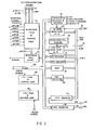
- microprocessor chip 10 (identified as a central processor unit or CPU in the figure) is interconnected via an appropriate system bus 11 with a memory system 12, one or more system I/0 units 17, one or more external microcontroller chips 13 (identified as "XMC" chips) and a system input/output interface unit 14 (identified as the system I/0 interface) and a further interface unit 14A (identified as ECLIPSE® I/O interface) which latter units interface with appropriate buses 15B and 15A for external input/output devices.
- the system is designed to operate with peripheral (I/0) units of the microNOVA type as used with microNOVA ® computer systems as made and sold by Data General Corporation of Westboro, Massachusetts and with peripheral (I/0) units of the ECLIPSE ® type as used with ECLIPSE ® computer systems made by Data General Corporation.
- peripheral (I/0) units of the microNOVA type as used with microNOVA ® computer systems as made and sold by Data General Corporation of Westboro, Massachusetts
- peripheral (I/0) units of the ECLIPSE ® type as used with ECLIPSE ® computer systems made by Data General Corporation.
- Information transfer i.e. addresses, data, instructions, etc
- system components other than the CPU such as one or more memory units and one or more input/output (I/0) devices
- I/0 input/output
- An effective system bus protocol must be utilised in order to provide for the correct transfer of such information. This aspect of the system is described in application No 83200686.0 published as EPO 094 140.
- the system CPU is arranged to be capable of communicating with I/O devices on a plurality of different buses.
- the CPU may communicate with I/0 devices directly on the system bus 11, with I/O devices on bus 15A designated in this embodiment, as the ECLIPSE ® I/O bus for ECLIPSE ® I/O devices, or on bus 15B designated in this embodiment as the MicroNOVA ® bus for microNOVA ® devices.
- data can be transferred directly to and from the system I/0 devices via the system bus 11, as described in more detail below, while data for ECLIPSE ® I/O devices are transferred to and from such devices via ECLIPSE® bus 15A through a separate ECLIPSE® I/O interface unit 45, the transfer thereof being controlled by control signals from the system I/O interface unit 14. Further, data for the microNOVA®I/O devices are transferred to and from such devices on the microNOVA®bus 15B through the system I/O interface unit.
- FIGS. 3 and 4 A more detailed block diagram of the system I/O interface unit 14 is shown in FIGS. 3 and 4.
- FIG. 5B A further, even more detailed, block diagram of the microNOVA®bus control logic for address/data transfers and for microNOVA polling operation (as discussed in more detail below) is shown in FIG. 5B.
- the system I/O interface unit comprises a plurality of local, or internal, devices and various control logic circuits, shown as block 50, the devices being of the type which are already known and used with respect to previously available systems.
- the internal devices of the system I/O interface unit 14 may include devices of the type utilized in the Data General Corporation ECLIPSEs computer systems, as shown and discussed with reference to the following publications:
- such devices may include a "programmable interval timer" (PIT) unit which provides a programmable timing signal which produces clock signals at a counter clock rate at one of four selectable frequencies, for example.
- PIT programmable interval timer
- the programmable interval time can be arranged to produce counter clock intervals at 1 MHz, 100 KHz, 10 KHz or 1 KHz from a constant input clock signal of 1 MHz through well-known frequency divider techniques.
- such timer responds to a pseudo-constant 1 MHz signal which is derived from a frequency synthesizer unit 51.
- the local devices may also include, for example, a "real time clock” (RTC) unit which generates timing pulses that are independent of the system clock rate.
- RTC real time clock
- the real time clock can interrupt at any one of four selectable frequencies, for example, at the AC line frequency, or at 10 Hz, 100 Hz or 1000 Hz the latter three clocks all derived from the pseudo-constant 1 MHz signal through well-known frequency divider techniques.
- the internal devices may also include a power monitor unit which detects any transition of a power monitor pulse which indicates that AC power has failed or that AC power has returned after a momentary power failure, or that a start up power condition exists.
- the system I/O interface unit also includes appropriate input and output interface logic via which serial data can be asynchronously supplied (as from a teletype unit, for example) , such inputs and outputs being supplied via TTI pin 55 and TTO pin 56, respectively, and from input and output registers 57 and 58, respectively, in a controlled manner in accordance with standard practice uitilizing suitable finite state machine (FSM) and control logic 59 and 60.
- FSM finite state machine
- the terminal unit may operate at selectable baud rates, the available baud rates being selected from a large number of such rates ranging in a particular case from 50 baud to 38400 baud, for example.
- the baud rate signals are derived from a pseudo-constant 614,400 Hz master baud rate signal, also obtained from the frequency synthesizer unit 51.
- the selected baud rates can be obtained therefrom though suitable baud rate selection logic in accordance with well-known techniques of prior art systems which utilize such asynchronous,,serial data input and output operation.
- an appropriate random access memory (RAM) storage unit 61 may also be present on the system I/O interface unit for providing temporary storage space which may be used, for example, when performing console operations.
- RAM random access memory
- Such storage unit is of a well-known RAM type which can be formed to provide storage space of an appropriate size for the desired console use.
- a particular embodiment may be capable of storing a selected number of 16-bit words for such purpose.
- the RAM unit 61 does not form a part of the inventive aspects of the system I/O interface unit 14 and need not be discussed in more detail.
- non-maskable interrupt (NMI) register 62 for use as described in the aforesaid ECLIPSE® and microNOVA® documents may also be part of the system I/O interface unit 14 but does not form a part of the inventive aspects thereof and need not be described in further detail.
- NMI non-maskable interrupt
- Addresses and data are supplied to and from the system bus 11 at the system I/O interface unit 14 in the form of 16-bit words (MB 0-15) supplied at the physical address/data (PADS) pins 63.
- Suitable driver and multiplexer circuits 64 are utilized for such purpose, the address and data words which are being transferred to or from the system bus being supplied to internal U bus 65 for use in the system I/O interface unit 14 either directly via an internal bus 66 or indirectly via temporary address/data register 67 which may be used for temporary storage thereof before such addresses and data are supplied to the system I/O interface unit or to the system bus depending on the direction of transfer thereof.
- the I/O buses which must be used to transfer addresses and data between the CPU and the I/O devices with which the CPU may desire communication differ depending on which type of I/O devices are involved (e.g., ECLIPSE devices which communicate via ECLIPSE bus 15A, microNOVA® devices which communicate via microNOVA bus 15B and all other devices which communicate via system bus 11).
- ECLIPSE devices which communicate via ECLIPSE bus 15A
- microNOVA® devices which communicate via microNOVA bus 15B and all other devices which communicate via system bus 11
- the system I/O interface unit 14 must decide which I/O device is involved and, hence, which I/O bus is to be used for the transfer of such data so that the interface unit control can control such transfer to and from the CPU.
- the system I/O interface unit 14 contains logic circuitry for identifying all of the devices which are on a selected one of the two buses which it controls, namely, buses 15A and 15B. Such identification can be achieved by appropriately “polling" the selected one of such buses and storing suitable information as to which devices are on the selected bus.
- the system I/O interface unit is arranged to "poll" the microNOWA® I/O bus 15B to determine which devices are on such bus.
- a suitable microNOV® poll counter 68 supplies each of the expected device code words which identify the various devices which are likely to be used with the system, which device code words, for example, are 6-bit device codes supplied to the microNOV® I/O bus 15B via "low-byte" (a byte is 8 bits) shift register 69 from poll counter 68 to the output microNOVA® bus pin 70 identified as IOD2 in FIG. 3.
- the 6-bit device codes are supplied in parallel to shift register (S/R) 69 during the polling process and are in turn supplied serially to the microNOVA®) bus from shift register 69.
- microNOVA I/O devices which communicate with the CPU on the microNOVA® bus 15B, are interrogated with a device code signal for identification thereof, such devices supply a return identifiable I/O clock (IOCLK) signal at pin 71 to microNOVA finite state machine and control logic 72 if a device matching a particular device code is present on the microNOVA bus.
- IOCLK return identifiable I/O clock
- Such operation is in contrast with devices on the ECLIPSE bus 15A for which no such identifiable I/O clock signal would be present if such devices were interrogated with the device codes. Because of such contrasting operations microNOVA® devices can be "polled” to determine their presence on microNOVA® bus 15B and a record of their presence kept in the system I/O interface unit 14.
- receipt of an IOCLK signal at pin 71 from a particular I/O device on the microNOVA®bus is supplied to control logic in the micmNOVA® finite state machine and control logic unit 72.
- Such logic generates a microNOVA exist signal (sometimes referred to as ⁇ NEXST) for supply to a microNOVA®poll register 73 to indicate that an I/O device having such device code is present on the microNOVA® bus.
- the microNOVA® poll store register 73 for example, is a 64-bit register, each bit correspondong to a particular device code (in particular embodiment there being up to 64 possible microNOVA® devices which can be present on the microNOVA® bus). If a 6-bit device code representing a specified device which has been interrogated is provided at the input thereto from microNOVA® poll counter 68, the particular bit associated therewith will be placed in a state which indicates the presence or absence of such device on the microNOVA® bus, depending on whether a UNEXST signal is so generated. Accordingly, when all of the device codes have been polled, the microNOVA® poll register 73 contains information as to the presence of all devices which are on the microNOVA® I/O bus 15B.
- Polling of the microNOVA bus is first performed at "start-up", the complete set of 64 possible devices in a particular embodiment, for example, being polled during one overall polling time interval before the ovarall system is put into operation. If, for example, the polling of each device takes 10 microseconds, or less, the complete poll can be accomplished in 600-700 microseconds. Once the system is in operation, updating of the poll store can be accomplished as devices previously indicated as not being present are turned on and devices previously indicated as present are turned off. Such updated polling can be accomplished at a 100 Hz rate, a single device being polled each .01 seconds (a completed update polling of all devices occurs every 0.6-0.7 seconds, for example).
- a device will be turned on and could, therefore, be present on the microNOVA® bus but the poll store may not indicate its presence (the updating for such device may not yet have occured since the device came on line after the last update poll. If, under such condition, the device requests an interrupt operation, the interrupt request itself indicates the presence of the device and the microNOVA® poll register is automatically updated by appropriate gating in the microNOVA finite state machine logic which provides a ⁇ LNEXST signal to the poll register.
- a jumper register 74 is arranged so that an ECLIPSE ENABLE and/or a microNOV® ENABLE is provided. The presence or absence thereof is controlled by the presence or absence of a suitable "jumper" connection being reflected by the state of the "jumper" register 72.
- the following chart summarizes the conditions for identifying the devices involved:
- the only devices identifiable are "system” devices.
- the system generates the ECLIPSE® timing signals (signified as "E") but the interface unit 14 does not determine whether the devices are ECLIPSE or system devices.
- the microNOVA® jumper is enabled but the ECLIPSE jumper is not, both microNOVA® and system devices are identifiable.
- microNOVA® devices can be identified but the system interface unit does not determine whether the devices are ECLIPSE® or system devices (the ECLIPSES timing signals are generated).
- the polling technique permits the system I/O interface unit 14 to determine whether a particular I/O device must be communicated with either on the microNOVA® I/O bus or on one of the other buses. If a microNOVA® device is present on the microNOVA® bus, its presence is indicated by the microNOVA poll store unit 73 which provides a microNOVA sensor signal, ⁇ NSNSR, to modify the operation of a master control finite state machine 75 so that its next state of operation provides the necessary control signals to control the operation of the microNOVA® finite state machine 73 for microNOVA® operation. Control signals are shown in FIG. 5B for performing the polling process.
- the low byte shift register 69 is loaded with the device code at the assertion of LOAD POLL COUNTER by the microNOVA® FSM 72, the poll count beginning at a poll count signal PLWC which increments the poll counter.
- the high byte shift register is loaded with a suitable instruction which can be selected to produce the least effect on the system (e.g., an IOSKP instruction in which data in all registers remain unchanged, etc.) at the assertion of a LOAD INST signal. If a return IOCLK is received at pin 71 a ⁇ NEXST signal is asserted by the microNOVA® FSM 72 which signal, together with the device code applied to the address latch of the poll store 73, provides the indication of the presence of the particular device involved. When the complete poll count is completed for start-up, for example, a POLDNE signal is asserted by poll counter 68 for supply to the microNOVA® FSM 73.
- the PLWR signal is used on "interrupts" by a device when the CPU acknowledges the interrupt request by such device by assertingan interrupt acknowledge signal.
- the devide itself updates the poll store, via the supplying of its device code and the supplying of the PLWR signal by the master control PSM to the poll store.
- the poll store For a poll store read operation, when an ADREN signal occurs, the poll store is accessed by the device code if an I/O instruction is present. The poll store then provides a ⁇ NSNSR signal to the master control FSM is such device is present.
- a poll update request signal (pPUR) is supplied from the master control FSM 75 at the 100 Hz rate as determined by a 100 Hz input counter signal.
- microNOVA 0 instruction register and decode logic 76 and the microNOVA® high byte register 77 for supplying the high byte at microNOVA®bus pin 78 are also shown in FIGS. 5A and 5B, as well as D-register 79 for shifting data to and from the U bus 65 and the microNOVA shifters 69 and 77, in accordance with standard microNOVA operation already well known to the art.
- Specific logic for the microNOVA FSM and control logic unit 72 and the master control FSM and control logic unit 75 are shown in Figs 5 and 6, respectively.
- the poll counter 68 and shift registers 69 and 77 are shown in Fig 7, while the poll store register 73 is shown in Fig 8.
- the system I/0 interface unit 14 is designed so as to be capable of operation at more than one input system clock frequency and is, therefore, adaptable for use with a system wherein the system clock is not expected to remain at a single fixed frequency for all operations.
- the frequency synthesizer unit 51 is provided so as to be responsive to one of a plurality of different selected input frequencies to produce the desired internal clock frequency required for operation of the internal devices of the interface unit and the desired master baud rate signal for operation of the asynchronous terminal system.
- the internal clock signal must have a substantially constant frequency of 1 MHz so as to provide for correct operation of the internal, or local, devices (such as the PIT and RTC devices mentioned above) and a substantially constant selected baud rate derived from the substantially constant master baud rate signal for the asynchronous terminal input/output logic.
Abstract
Description
- The present invention relates to a data processing system having a central processor unit and a system bus for providing communication with one or more memory units, first and second interfaces providing communication between the system bus and a first and second input/output buses in further communication with first and second groups respectively of external units and wherein at least one interface stores a table of external devices addressable thereby.
- Such a system is known from "Hardware considerations in a micro-computer multiprocessing system" Baum and Senzig, IEEE Computer Society International Conference Comp Con 25/27 February 1975, pages 27 to 30. This reference describes a system in which "bus links" i.e. interfaces, are used to interface a system bus to input/output buses. Each bus link has to be set up with its own table of device addresses which it can service. The object of the present invention is to provide an improved system which automates the determination of which input/output bus is to be employed, particularly in the specific context of utilising two buses to cater for different devices having different bus characteristics. A further object is to provide a system which can adapt continuously to the changing situation of which devices are active on which bus.
- The present invention is characterised in that the second interface includes a control signal connection to the first interface, means for polling the devices on the second input/output bus to identify each of the external devices of the second group which are currently in communication with the second input/output bus, means for storing information which indicates the thus identified external devices of the second group, and means responsive to the stored information for controlling the operation of the second interface to provide access to the identified external devices via the second input/output bus and to provide access to external devices on the first input/output bus when such devices are not identified as on the second bus.
- The invention will now be described in more detail, by way of example, with reference to the accompanying drawings, in which:
- Fig 1 is a broad block diagram of an overall system in accordance with the invention;
- Figs 2 and 3 are block diagrams of the system I/O interface unit of Fig 1;
- Fig 4 is a more specific block diagram of a portion of the system I/O interface unit of Figs 2 and 3;
- Fig 5 is a more specific logic diagram of the master control finite state machine and control logic of Figs 2 and 3;
- Fig 6 is a more specific logic diagram of the microNOVA finite state machine and control logic of Figs 2 and 3; and
- Figs 7 and 8 show more specific logic diagrams of the microNOVA polling logic of Figs 2 to 4.
- An overall system using the techniques of the invention is shown in Fig 1 wherein microprocessor chip 10 (identified as a central processor unit or CPU in the figure) is interconnected via an appropriate system bus 11 with a
memory system 12, one or more system I/0units 17, one or more external microcontroller chips 13 (identified as "XMC" chips) and a system input/output interface unit 14 (identified as the system I/0 interface) and afurther interface unit 14A (identified as ECLIPSE® I/O interface) which latter units interface withappropriate buses 15B and 15A for external input/output devices. For example, in a particular embodiment the system is designed to operate with peripheral (I/0) units of the microNOVA type as used with microNOVA ® computer systems as made and sold by Data General Corporation of Westboro, Massachusetts and with peripheral (I/0) units of the ECLIPSE ® type as used with ECLIPSE ® computer systems made by Data General Corporation. - Information transfer (i.e. addresses, data, instructions, etc) to and from the CPU from system components other than the CPU, such as one or more memory units and one or more input/output (I/0) devices, takes place on the 16-bit system bus 11 either directly or via
interface units - The system CPU is arranged to be capable of communicating with I/O devices on a plurality of different buses. Thus, the CPU may communicate with I/0 devices directly on the system bus 11, with I/O devices on
bus 15A designated in this embodiment, as the ECLIPSE ® I/O bus for ECLIPSE ® I/O devices, or on bus 15B designated in this embodiment as the MicroNOVA ® bus for microNOVA ® devices. In accordance with the system described herein, data can be transferred directly to and from the system I/0 devices via the system bus 11, as described in more detail below, while data for ECLIPSE ® I/O devices are transferred to and from such devices via ECLIPSE®bus 15A through a separate ECLIPSE® I/O interface unit 45, the transfer thereof being controlled by control signals from the system I/O interface unit 14. Further, data for the microNOVA®I/O devices are transferred to and from such devices on the microNOVA®bus 15B through the system I/O interface unit. - A more detailed block diagram of the system I/
O interface unit 14 is shown in FIGS. 3 and 4. A further, even more detailed, block diagram of the microNOVA®bus control logic for address/data transfers and for microNOVA polling operation (as discussed in more detail below) is shown in FIG. 5B. As can be seen therein, the system I/O interface unit comprises a plurality of local, or internal, devices and various control logic circuits, shown asblock 50, the devices being of the type which are already known and used with respect to previously available systems. For example, the internal devices of the system I/O interface unit 14 may include devices of the type utilized in the Data General Corporation ECLIPSEs computer systems, as shown and discussed with reference to the following publications:
- The above publications are representative of publications available from Data General Corporation, Westboro, Massachusetts concerning NOVA , ECLIPSE®, and microNOVA systems made and sold by Data General Corporation. Such publications contain information useful as background information in understanding not only the aforementioned internal devices but also various other aspects of the system being described herein.
- Thus, such devices may include a "programmable interval timer" (PIT) unit which provides a programmable timing signal which produces clock signals at a counter clock rate at one of four selectable frequencies, for example. In a particular embodiment, for example, the programmable interval time can be arranged to produce counter clock intervals at 1 MHz, 100 KHz, 10 KHz or 1 KHz from a constant input clock signal of 1 MHz through well-known frequency divider techniques. In the system I/O unit, such timer responds to a pseudo-constant 1 MHz signal which is derived from a
frequency synthesizer unit 51. - The local devices may also include, for example, a "real time clock" (RTC) unit which generates timing pulses that are independent of the system clock rate. The real time clock can interrupt at any one of four selectable frequencies, for example, at the AC line frequency, or at 10 Hz, 100 Hz or 1000 Hz the latter three clocks all derived from the pseudo-constant 1 MHz signal through well-known frequency divider techniques.
- The internal devices may also include a power monitor unit which detects any transition of a power monitor pulse which indicates that AC power has failed or that AC power has returned after a momentary power failure, or that a start up power condition exists.
- The system I/O interface unit also includes appropriate input and output interface logic via which serial data can be asynchronously supplied (as from a teletype unit, for example) , such inputs and outputs being supplied via
TTI pin 55 andTTO pin 56, respectively, and from input andoutput registers control logic frequency synthesizer unit 51. The selected baud rates can be obtained therefrom though suitable baud rate selection logic in accordance with well-known techniques of prior art systems which utilize such asynchronous,,serial data input and output operation. - The internal units and the terminal logic discussed above do not form a part of the inventive aspects of the system I/
O interface unit 14 and need not be described in further detail. - For convenience, an appropriate random access memory (RAM)
storage unit 61 may also be present on the system I/O interface unit for providing temporary storage space which may be used, for example, when performing console operations. Such storage unit is of a well-known RAM type which can be formed to provide storage space of an appropriate size for the desired console use. For example, a particular embodiment may be capable of storing a selected number of 16-bit words for such purpose. As such, theRAM unit 61 does not form a part of the inventive aspects of the system I/O interface unit 14 and need not be discussed in more detail. Further a non-maskable interrupt (NMI)register 62 for use as described in the aforesaid ECLIPSE® and microNOVA® documents may also be part of the system I/O interface unit 14 but does not form a part of the inventive aspects thereof and need not be described in further detail. - Addresses and data are supplied to and from the system bus 11 at the system I/
O interface unit 14 in the form of 16-bit words (MB 0-15) supplied at the physical address/data (PADS)pins 63. Suitable driver andmultiplexer circuits 64 are utilized for such purpose, the address and data words which are being transferred to or from the system bus being supplied tointernal U bus 65 for use in the system I/O interface unit 14 either directly via aninternal bus 66 or indirectly via temporary address/data register 67 which may be used for temporary storage thereof before such addresses and data are supplied to the system I/O interface unit or to the system bus depending on the direction of transfer thereof. - The I/O buses which must be used to transfer addresses and data between the CPU and the I/O devices with which the CPU may desire communication differ depending on which type of I/O devices are involved (e.g., ECLIPSE devices which communicate via ECLIPSE
bus 15A, microNOVA® devices which communicate via microNOVA bus 15B and all other devices which communicate via system bus 11). The system I/O interface unit 14 must decide which I/O device is involved and, hence, which I/O bus is to be used for the transfer of such data so that the interface unit control can control such transfer to and from the CPU. In accordance with the system of the invention disclosed in FIGS. 2 and 3, and the more detailed block diagram of FIG. 4, the system I/O interface unit 14 contains logic circuitry for identifying all of the devices which are on a selected one of the two buses which it controls, namely,buses 15A and 15B. Such identification can be achieved by appropriately "polling" the selected one of such buses and storing suitable information as to which devices are on the selected bus. - In accordance with a specific embodiment of the invention which utilizes either a microNOVA® I/O bus 15B or an ECLIPSE® I/
O bus 15A, the system I/O interface unit is arranged to "poll" the microNOWA® I/O bus 15B to determine which devices are on such bus. A suitable microNOV®poll counter 68 supplies each of the expected device code words which identify the various devices which are likely to be used with the system, which device code words, for example, are 6-bit device codes supplied to the microNOV® I/O bus 15B via "low-byte" (a byte is 8 bits)shift register 69 frompoll counter 68 to the output microNOVA®bus pin 70 identified as IOD2 in FIG. 3. The 6-bit device codes are supplied in parallel to shift register (S/R) 69 during the polling process and are in turn supplied serially to the microNOVA®) bus fromshift register 69. - When microNOVA I/O devices, which communicate with the CPU on the microNOVA® bus 15B, are interrogated with a device code signal for identification thereof, such devices supply a return identifiable I/O clock (IOCLK) signal at
pin 71 to microNOVA finite state machine andcontrol logic 72 if a device matching a particular device code is present on the microNOVA bus. Such operation is in contrast with devices on the ECLIPSEbus 15A for which no such identifiable I/O clock signal would be present if such devices were interrogated with the device codes. Because of such contrasting operations microNOVA® devices can be "polled" to determine their presence on microNOVA® bus 15B and a record of their presence kept in the system I/O interface unit 14. - Thus, receipt of an IOCLK signal at
pin 71 from a particular I/O device on the microNOVA®bus is supplied to control logic in the micmNOVA® finite state machine andcontrol logic unit 72. Such logic generates a microNOVA exist signal (sometimes referred to as µNEXST) for supply to a microNOVA®poll register 73 to indicate that an I/O device having such device code is present on the microNOVA® bus. - The microNOVA®
poll store register 73, for example, is a 64-bit register, each bit correspondong to a particular device code (in particular embodiment there being up to 64 possible microNOVA® devices which can be present on the microNOVA® bus). If a 6-bit device code representing a specified device which has been interrogated is provided at the input thereto from microNOVA®poll counter 68, the particular bit associated therewith will be placed in a state which indicates the presence or absence of such device on the microNOVA® bus, depending on whether a UNEXST signal is so generated. Accordingly, when all of the device codes have been polled, the microNOVA®poll register 73 contains information as to the presence of all devices which are on the microNOVA® I/O bus 15B. - Polling of the microNOVA bus is first performed at "start-up", the complete set of 64 possible devices in a particular embodiment, for example, being polled during one overall polling time interval before the ovarall system is put into operation. If, for example, the polling of each device takes 10 microseconds, or less, the complete poll can be accomplished in 600-700 microseconds. Once the system is in operation, updating of the poll store can be accomplished as devices previously indicated as not being present are turned on and devices previously indicated as present are turned off. Such updated polling can be accomplished at a 100 Hz rate, a single device being polled each .01 seconds (a completed update polling of all devices occurs every 0.6-0.7 seconds, for example).
- In some cases a device will be turned on and could, therefore, be present on the microNOVA® bus but the poll store may not indicate its presence (the updating for such device may not yet have occured since the device came on line after the last update poll. If, under such condition, the device requests an interrupt operation, the interrupt request itself indicates the presence of the device and the microNOVA® poll register is automatically updated by appropriate gating in the microNOVA finite state machine logic which provides a µLNEXST signal to the poll register.
- All devices which are not identified as being on the microNOVA I/O bus, but which are in communication with the system, will by the process of elimination be either on the ECLIPSE ® I/
O bus 15A or on the system bus 11. As will be noted, ajumper register 74 is arranged so that an ECLIPSE ENABLE and/or a microNOV® ENABLE is provided. The presence or absence thereof is controlled by the presence or absence of a suitable "jumper" connection being reflected by the state of the "jumper"register 72. The following chart summarizes the conditions for identifying the devices involved:
- In the first condition where neither jumper connection is enabled the only devices identifiable are "system" devices. Where the ECLIPSE® jumper is enabled but the microNOV® jumper is not, the system generates the ECLIPSE® timing signals (signified as "E") but the
interface unit 14 does not determine whether the devices are ECLIPSE or system devices. Where the microNOVA® jumper is enabled but the ECLIPSE jumper is not, both microNOVA® and system devices are identifiable. Where both jumpers are enabled, microNOVA® devices can be identified but the system interface unit does not determine whether the devices are ECLIPSE® or system devices (the ECLIPSES timing signals are generated). Accordingly, the polling technique permits the system I/O interface unit 14 to determine whether a particular I/O device must be communicated with either on the microNOVA® I/O bus or on one of the other buses. If a microNOVA® device is present on the microNOVA® bus, its presence is indicated by the microNOVApoll store unit 73 which provides a microNOVA sensor signal, µNSNSR, to modify the operation of a master controlfinite state machine 75 so that its next state of operation provides the necessary control signals to control the operation of the microNOVA®finite state machine 73 for microNOVA® operation. Control signals are shown in FIG. 5B for performing the polling process. The lowbyte shift register 69 is loaded with the device code at the assertion of LOAD POLL COUNTER by themicroNOVA® FSM 72, the poll count beginning at a poll count signal PLWC which increments the poll counter. The high byte shift register is loaded with a suitable instruction which can be selected to produce the least effect on the system (e.g., an IOSKP instruction in which data in all registers remain unchanged, etc.) at the assertion of a LOAD INST signal. If a return IOCLK is received at pin 71 a µNEXST signal is asserted by themicroNOVA® FSM 72 which signal, together with the device code applied to the address latch of thepoll store 73, provides the indication of the presence of the particular device involved. When the complete poll count is completed for start-up, for example, a POLDNE signal is asserted by poll counter 68 for supply to themicroNOVA® FSM 73. - The PLWR signal is used on "interrupts" by a device when the CPU acknowledges the interrupt request by such device by assertingan interrupt acknowledge signal. At the assertion of a suitable interrupt acknowledge signal the devide itself updates the poll store, via the supplying of its device code and the supplying of the PLWR signal by the master control PSM to the poll store.
- For a poll store read operation, when an ADREN signal occurs, the poll store is accessed by the device code if an I/O instruction is present. The poll store then provides a µNSNSR signal to the master control FSM is such device is present.
- A poll update request signal (pPUR) is supplied from the
master control FSM 75 at the 100 Hz rate as determined by a 100 Hz input counter signal. - The required microNOVA 0 instruction register and decode
logic 76 and the microNOVA®high byte register 77 for supplying the high byte at microNOVA®bus pin 78 (IODI) are also shown in FIGS. 5A and 5B, as well as D-register 79 for shifting data to and from theU bus 65 and themicroNOVA shifters logic unit 72 and the master control FSM and controllogic unit 75 are shown in Figs 5 and 6, respectively. Thepoll counter 68 andshift registers poll store register 73 is shown in Fig 8. - The system I/0
interface unit 14 is designed so as to be capable of operation at more than one input system clock frequency and is, therefore, adaptable for use with a system wherein the system clock is not expected to remain at a single fixed frequency for all operations. Thefrequency synthesizer unit 51 is provided so as to be responsive to one of a plurality of different selected input frequencies to produce the desired internal clock frequency required for operation of the internal devices of the interface unit and the desired master baud rate signal for operation of the asynchronous terminal system. In a particular embodiment, for example, the internal clock signal must have a substantially constant frequency of 1 MHz so as to provide for correct operation of the internal, or local, devices (such as the PIT and RTC devices mentioned above) and a substantially constant selected baud rate derived from the substantially constant master baud rate signal for the asynchronous terminal input/output logic. - A full description of the frequency synthesis unit is contained in
EP 0 035 334 (and in application No 83200684 =EP 0 097 977 which, like the present application and application 83200686.0 =EP 0 094 140 is divided out of 81300560, published asEP 0 035 334).
Claims (3)
Applications Claiming Priority (8)
| Application Number | Priority Date | Filing Date | Title |
|---|---|---|---|
| US12029280A | 1980-02-11 | 1980-02-11 | |
| US120292 | 1980-02-11 | ||
| US120291 | 1980-02-11 | ||
| US06/120,271 US4371925A (en) | 1980-02-11 | 1980-02-11 | Data processing system having unique bus control operation |
| US120271 | 1980-02-11 | ||
| US06/120,272 US4394736A (en) | 1980-02-11 | 1980-02-11 | Data processing system utilizing a unique two-level microcoding technique for forming microinstructions |
| US120272 | 1980-02-11 | ||
| US06/120,291 US4464772A (en) | 1980-02-11 | 1980-02-11 | Frequency synthesizer for providing a pseudo-constant frequency signal |
Related Parent Applications (2)
| Application Number | Title | Priority Date | Filing Date |
|---|---|---|---|
| EP81300560A Division-Into EP0035334B1 (en) | 1980-02-11 | 1981-02-11 | Data processing system with two level microprogramming |
| EP81300560A Division EP0035334B1 (en) | 1980-02-11 | 1981-02-11 | Data processing system with two level microprogramming |
Publications (2)
| Publication Number | Publication Date |
|---|---|
| EP0164138A1 true EP0164138A1 (en) | 1985-12-11 |
| EP0164138B1 EP0164138B1 (en) | 1989-08-16 |
Family
ID=27494306
Family Applications (4)
| Application Number | Title | Priority Date | Filing Date |
|---|---|---|---|
| EP85200462A Expired EP0164138B1 (en) | 1980-02-11 | 1981-02-11 | Data processing system with a plurality of input/output buses |
| EP83200684A Expired EP0097977B1 (en) | 1980-02-11 | 1981-02-11 | Frequency synthesizer |
| EP83200686A Withdrawn EP0094140A1 (en) | 1980-02-11 | 1981-02-11 | Data processing system with system bus for transfer of information |
| EP81300560A Expired EP0035334B1 (en) | 1980-02-11 | 1981-02-11 | Data processing system with two level microprogramming |
Family Applications After (3)
| Application Number | Title | Priority Date | Filing Date |
|---|---|---|---|
| EP83200684A Expired EP0097977B1 (en) | 1980-02-11 | 1981-02-11 | Frequency synthesizer |
| EP83200686A Withdrawn EP0094140A1 (en) | 1980-02-11 | 1981-02-11 | Data processing system with system bus for transfer of information |
| EP81300560A Expired EP0035334B1 (en) | 1980-02-11 | 1981-02-11 | Data processing system with two level microprogramming |
Country Status (6)
| Country | Link |
|---|---|
| EP (4) | EP0164138B1 (en) |
| JP (1) | JPS6319854Y2 (en) |
| AU (3) | AU541189B2 (en) |
| BR (1) | BR8100790A (en) |
| DE (3) | DE3175667D1 (en) |
| IL (1) | IL62055A (en) |
Cited By (4)
| Publication number | Priority date | Publication date | Assignee | Title |
|---|---|---|---|---|
| EP0260392A2 (en) * | 1986-09-19 | 1988-03-23 | International Business Machines Corporation | An input output interface controller connecting a synchronous bus to an asynchronous bus and methods for performing operations on the buses |
| US5199106A (en) * | 1986-09-19 | 1993-03-30 | International Business Machines Corporation | Input output interface controller connecting a synchronous bus to an asynchronous bus and methods for performing operations on the bus |
| EP0594024A1 (en) * | 1992-10-23 | 1994-04-27 | International Business Machines Corporation | Method and apparatus for enabling data paths on a remote bus |
| EP1990725A1 (en) * | 2006-02-27 | 2008-11-12 | Fujitsu Ltd. | Central processing unit, central processing unit control method, and information processing system |
Families Citing this family (11)
| Publication number | Priority date | Publication date | Assignee | Title |
|---|---|---|---|---|
| AU541189B2 (en) | 1980-02-11 | 1984-12-20 | Data General Corporation | Data processing system |
| US4476527A (en) * | 1981-12-10 | 1984-10-09 | Data General Corporation | Synchronous data bus with automatically variable data rate |
| FR2538140B1 (en) * | 1982-12-21 | 1988-06-24 | Thomson Csf Mat Tel | BUS COUPLING DEVICE FOR MULTIPLE BUS DATA PROCESSING SYSTEM |
| US4837785A (en) * | 1983-06-14 | 1989-06-06 | Aptec Computer Systems, Inc. | Data transfer system and method of operation thereof |
| US4817037A (en) * | 1987-02-13 | 1989-03-28 | International Business Machines Corporation | Data processing system with overlap bus cycle operations |
| JPH0276056A (en) * | 1988-09-13 | 1990-03-15 | Toshiba Corp | Information processor |
| CA2007737C (en) * | 1989-02-24 | 1998-04-28 | Paul Samuel Gallo | Data transfer operations between two asynchronous buses |
| WO1993016434A1 (en) * | 1992-02-13 | 1993-08-19 | Tandy Corporation | Method and apparatus to reduce computer system bus interleave overhead |
| FR2716053B1 (en) * | 1994-02-09 | 1996-04-26 | Sat | Method for generating a specific frequency by dividing a reference frequency. |
| JP3016179B2 (en) * | 1995-06-27 | 2000-03-06 | るいエンジニアリング株式会社 | Swivel for drilling machine |
| US20190158127A1 (en) * | 2017-11-23 | 2019-05-23 | M31 Technology Corporation | Encoding and decoding architecture for high-speed data communication system and related physical layer circuit, transmitter and receiver and communication system thereof |
Citations (1)
| Publication number | Priority date | Publication date | Assignee | Title |
|---|---|---|---|---|
| US4000485A (en) * | 1975-06-30 | 1976-12-28 | Honeywell Information Systems, Inc. | Data processing system providing locked operation of shared resources |
Family Cites Families (16)
| Publication number | Priority date | Publication date | Assignee | Title |
|---|---|---|---|---|
| FR1188034A (en) * | 1957-11-21 | 1959-09-18 | Trt Telecom Radio Electr | Means of intercorrelation for several stations transmitting information |
| US3221307A (en) * | 1960-12-07 | 1965-11-30 | Ibm | Automatic tape unit selector |
| US3217267A (en) * | 1963-10-02 | 1965-11-09 | Ling Temco Vought Inc | Frequency synthesis using fractional division by digital techniques within a phase-locked loop |
| DE1958662B2 (en) * | 1969-11-22 | 1971-12-30 | Siemens AG, 1000 Berlin u. 8000 München | DIGITAL PULSE SEQUENCE DIVIDER WITH OPTIMAL EQUAL DISTRIBUTION OF THE PULSE OF AN OUTPUT PULSE SEQUENCE SELECTED FROM AN AEQUIDISTANT INPUT PULSE SEQUENCE |
| US3786434A (en) * | 1972-12-20 | 1974-01-15 | Ibm | Full capacity small size microprogrammed control unit |
| JPS5250112B2 (en) * | 1973-06-07 | 1977-12-22 | ||
| DE2336676C3 (en) * | 1973-07-19 | 1981-06-19 | Ibm Deutschland Gmbh, 7000 Stuttgart | Device for modifying microprogram instructions |
| IT995721B (en) * | 1973-10-10 | 1975-11-20 | Honeywell Inf Systems Italia | EQUIPMENT FOR THE INTERPRETATION OF FUNCTION CODES IN MICROPROGRAMMED COMPUTERS AND FOR THE INDEPENDENT ADDRESSING OF INTERPRETATIVE AND EXECUTIVE PHASES OF MICRO PROGRAM |
| DE2510766A1 (en) * | 1975-03-12 | 1977-02-17 | Schlafhorst & Co W | METHOD AND DEVICE FOR THE INDEPENDENT DIGITAL DIVISION OF A FREQUENCY |
| US3997896A (en) * | 1975-06-30 | 1976-12-14 | Honeywell Information Systems, Inc. | Data processing system providing split bus cycle operation |
| JPS538034A (en) * | 1976-06-30 | 1978-01-25 | Toshiba Corp | Electronic computer |
| US4081755A (en) * | 1976-08-10 | 1978-03-28 | Litton Business Systems, Inc. | Baud rate generator utilizing single clock source |
| US4084082A (en) * | 1976-10-12 | 1978-04-11 | Fairchild Camera And Instrument Corporation | Programmable counter |
| US4186379A (en) * | 1977-04-28 | 1980-01-29 | Hewlett-Packard Company | High-speed data transfer apparatus |
| US4148011A (en) * | 1977-06-06 | 1979-04-03 | General Automation, Inc. | Asynchronous priority circuit for controlling access to a bus |
| AU541189B2 (en) | 1980-02-11 | 1984-12-20 | Data General Corporation | Data processing system |
-
1981
- 1981-01-30 AU AU66790/81A patent/AU541189B2/en not_active Ceased
- 1981-02-03 IL IL62055A patent/IL62055A/en unknown
- 1981-02-09 BR BR8100790A patent/BR8100790A/en not_active IP Right Cessation
- 1981-02-11 EP EP85200462A patent/EP0164138B1/en not_active Expired
- 1981-02-11 EP EP83200684A patent/EP0097977B1/en not_active Expired
- 1981-02-11 EP EP83200686A patent/EP0094140A1/en not_active Withdrawn
- 1981-02-11 DE DE8383200684T patent/DE3175667D1/en not_active Expired
- 1981-02-11 DE DE8181300560T patent/DE3172395D1/en not_active Expired
- 1981-02-11 DE DE8585200462T patent/DE3177087D1/en not_active Expired
- 1981-02-11 EP EP81300560A patent/EP0035334B1/en not_active Expired
-
1985
- 1985-02-22 AU AU39100/85A patent/AU573310B2/en not_active Ceased
-
1987
- 1987-06-08 JP JP1987088478U patent/JPS6319854Y2/ja not_active Expired
-
1988
- 1988-03-28 AU AU13805/88A patent/AU1380588A/en not_active Abandoned
Patent Citations (1)
| Publication number | Priority date | Publication date | Assignee | Title |
|---|---|---|---|---|
| US4000485A (en) * | 1975-06-30 | 1976-12-28 | Honeywell Information Systems, Inc. | Data processing system providing locked operation of shared resources |
Non-Patent Citations (3)
| Title |
|---|
| IEEE COMPUTER SOCIETY INTERNATIONAL CONFERENCE, COMPCON 75, 25th-27th February 1975, San Francisco, pages 27-30, New York, US; A.BAUM et al.: "Hardware considerations in a microcomputer multiprocessing system" * |
| IEEE TRANSACTIONS ON NUCLEAR SCIENCE, vol. NS-26, no. 1, February 1979, pages 679-685, New York, US; R.S.LARSEN: "Status of the interlaboratory development of a high-speed standard data bus - fastbus" * |
| IEEE TRANSACTIONS ON NUCLEAR SCIENCE, vol. NS-26, no. 4, August 1979, pages 4525-4530, New York, US; R.W.DOWNING: "Fastbus - Details of addressing and bus mastership" * |
Cited By (9)
| Publication number | Priority date | Publication date | Assignee | Title |
|---|---|---|---|---|
| EP0260392A2 (en) * | 1986-09-19 | 1988-03-23 | International Business Machines Corporation | An input output interface controller connecting a synchronous bus to an asynchronous bus and methods for performing operations on the buses |
| EP0260392A3 (en) * | 1986-09-19 | 1992-03-11 | International Business Machines Corporation | An input output interface controller connecting a synchronous bus to an asynchronous bus and methods for performing operations on the buses |
| US5199106A (en) * | 1986-09-19 | 1993-03-30 | International Business Machines Corporation | Input output interface controller connecting a synchronous bus to an asynchronous bus and methods for performing operations on the bus |
| US5276814A (en) * | 1986-09-19 | 1994-01-04 | International Business Machines Corporation | Method for transferring information between main store and input output bus units via a sequence of asynchronous bus and two synchronous buses |
| EP0594024A1 (en) * | 1992-10-23 | 1994-04-27 | International Business Machines Corporation | Method and apparatus for enabling data paths on a remote bus |
| US5655112A (en) * | 1992-10-23 | 1997-08-05 | International Business Machines Corporation | Method and apparatus for enabling data paths on a remote bus |
| EP1990725A1 (en) * | 2006-02-27 | 2008-11-12 | Fujitsu Ltd. | Central processing unit, central processing unit control method, and information processing system |
| EP1990725A4 (en) * | 2006-02-27 | 2010-08-25 | Fujitsu Ltd | Central processing unit, central processing unit control method, and information processing system |
| US8015326B2 (en) | 2006-02-27 | 2011-09-06 | Fujitsu Limited | Central processing apparatus, control method therefor and information processing system |
Also Published As
| Publication number | Publication date |
|---|---|
| AU1380588A (en) | 1988-06-23 |
| EP0035334A3 (en) | 1981-12-09 |
| AU6679081A (en) | 1981-09-03 |
| AU3910085A (en) | 1985-09-05 |
| EP0035334B1 (en) | 1985-09-25 |
| EP0097977A2 (en) | 1984-01-11 |
| BR8100790A (en) | 1981-08-25 |
| EP0097977A3 (en) | 1984-02-15 |
| JPS6319854Y2 (en) | 1988-06-02 |
| EP0097977B1 (en) | 1986-11-26 |
| EP0164138B1 (en) | 1989-08-16 |
| DE3172395D1 (en) | 1985-10-31 |
| EP0035334A2 (en) | 1981-09-09 |
| IL62055A0 (en) | 1981-03-31 |
| IL62055A (en) | 1987-11-30 |
| DE3175667D1 (en) | 1987-01-15 |
| AU541189B2 (en) | 1984-12-20 |
| EP0094140A1 (en) | 1983-11-16 |
| AU573310B2 (en) | 1988-06-02 |
| DE3177087D1 (en) | 1989-09-21 |
| JPS6312231U (en) | 1988-01-27 |
Similar Documents
| Publication | Publication Date | Title |
|---|---|---|
| EP0164138B1 (en) | Data processing system with a plurality of input/output buses | |
| US4805137A (en) | Bus controller command block processing system | |
| US4519028A (en) | CPU with multi-stage mode register for defining CPU operating environment including charging its communications protocol | |
| US5455916A (en) | Method for performing inter-unit data transfer operations among a plurality of input/output bus interface units coupled to a common asynchronous bus | |
| US4964038A (en) | Data processing system having automatic address allocation arrangements for addressing interface cards | |
| US5021950A (en) | Multiprocessor system with standby function | |
| US4495571A (en) | Data processing system having synchronous bus wait/retry cycle | |
| US4674033A (en) | Multiprocessor system having a shared memory for enhanced interprocessor communication | |
| US4591973A (en) | Input/output system and method for digital computers | |
| US4079454A (en) | Data processing system using read-only-memory arrays to provide operation in a plurality of operating states | |
| US5715438A (en) | System and method for providing time base adjustment | |
| EP0071743A2 (en) | Refresh circuit for dynamic memory of a data processor employing a direct memory access controller | |
| EP0458304A1 (en) | Direct memory access transfer controller | |
| EP0230664A2 (en) | Master slave microprocessor system with virtual memory | |
| US4090239A (en) | Interval timer for use in an input/output system | |
| EP0464615A2 (en) | Microcomputer equipped with DMA controller | |
| JPS56159725A (en) | Module type data processor | |
| EP0234598A2 (en) | Interface circuit for subsystem controller | |
| US5175820A (en) | Apparatus for use with a computing device controlling communications with a plurality of peripheral devices including a feedback bus to indicate operational modes | |
| US5734924A (en) | System for host accessing local memory by asserting address signal corresponding to host adapter and data signal indicating address of location in local memory | |
| EP0380845A3 (en) | An interface between a system control unit and a service processing unit of a digital computer | |
| EP0306043B1 (en) | Storage of input/output command timeout and acknowledge responses | |
| EP0393290B1 (en) | Memory and peripheral chip select apparatus | |
| EP0712078A1 (en) | Data processor with transparent operation during a background mode and method therefor | |
| US4628445A (en) | Apparatus and method for synchronization of peripheral devices via bus cycle alteration in a microprocessor implemented data processing system |
Legal Events
| Date | Code | Title | Description |
|---|---|---|---|
| PUAI | Public reference made under article 153(3) epc to a published international application that has entered the european phase |
Free format text: ORIGINAL CODE: 0009012 |
|
| AC | Divisional application: reference to earlier application |
Ref document number: 35334 Country of ref document: EP |
|
| AK | Designated contracting states |
Designated state(s): CH DE FR GB IT LI NL SE |
|
| RIN1 | Information on inventor provided before grant (corrected) |
Inventor name: MARCH, ROGER W. Inventor name: BUCKLEY, EDWARD M. Inventor name: GUSOWSKI, RONALD I. Inventor name: DRUKE, MICHAEL B. Inventor name: CARBERRY, RICHARD A. Inventor name: BERNSTEIN, DAVID H. |
|
| RIN1 | Information on inventor provided before grant (corrected) |
Inventor name: MARCH, ROGER W. Inventor name: BUCKLEY, EDWARD M. Inventor name: GUSOWSKI, RONALD I. Inventor name: DRUKE, MICHAEL B. Inventor name: CARBERRY, RICHARD A. Inventor name: BERNSTEIN, DAVID H. |
|
| 17P | Request for examination filed |
Effective date: 19860530 |
|
| 17Q | First examination report despatched |
Effective date: 19880624 |
|
| ITTA | It: last paid annual fee | ||
| GRAA | (expected) grant |
Free format text: ORIGINAL CODE: 0009210 |
|
| AC | Divisional application: reference to earlier application |
Ref document number: 35334 Country of ref document: EP |
|
| AK | Designated contracting states |
Kind code of ref document: B1 Designated state(s): CH DE FR GB IT LI NL SE |
|
| PG25 | Lapsed in a contracting state [announced via postgrant information from national office to epo] |
Ref country code: SE Effective date: 19890816 Ref country code: NL Effective date: 19890816 Ref country code: LI Effective date: 19890816 Ref country code: IT Free format text: LAPSE BECAUSE OF FAILURE TO SUBMIT A TRANSLATION OF THE DESCRIPTION OR TO PAY THE FEE WITHIN THE PRESCRIBED TIME-LIMIT;WARNING: LAPSES OF ITALIAN PATENTS WITH EFFECTIVE DATE BEFORE 2007 MAY HAVE OCCURRED AT ANY TIME BEFORE 2007. THE CORRECT EFFECTIVE DATE MAY BE DIFFERENT FROM THE ONE RECORDED. Effective date: 19890816 Ref country code: CH Effective date: 19890816 |
|
| REF | Corresponds to: |
Ref document number: 3177087 Country of ref document: DE Date of ref document: 19890921 |
|
| ET | Fr: translation filed | ||
| REG | Reference to a national code |
Ref country code: CH Ref legal event code: PL |
|
| NLV1 | Nl: lapsed or annulled due to failure to fulfill the requirements of art. 29p and 29m of the patents act | ||
| PLBE | No opposition filed within time limit |
Free format text: ORIGINAL CODE: 0009261 |
|
| STAA | Information on the status of an ep patent application or granted ep patent |
Free format text: STATUS: NO OPPOSITION FILED WITHIN TIME LIMIT |
|
| 26N | No opposition filed | ||
| PGFP | Annual fee paid to national office [announced via postgrant information from national office to epo] |
Ref country code: GB Payment date: 19930108 Year of fee payment: 13 |
|
| PGFP | Annual fee paid to national office [announced via postgrant information from national office to epo] |
Ref country code: FR Payment date: 19930125 Year of fee payment: 13 |
|
| PGFP | Annual fee paid to national office [announced via postgrant information from national office to epo] |
Ref country code: DE Payment date: 19930127 Year of fee payment: 13 |
|
| PG25 | Lapsed in a contracting state [announced via postgrant information from national office to epo] |
Ref country code: GB Effective date: 19940211 |
|
| GBPC | Gb: european patent ceased through non-payment of renewal fee |
Effective date: 19940211 |
|
| PG25 | Lapsed in a contracting state [announced via postgrant information from national office to epo] |
Ref country code: FR Effective date: 19941031 |
|
| PG25 | Lapsed in a contracting state [announced via postgrant information from national office to epo] |
Ref country code: DE Effective date: 19941101 |
|
| REG | Reference to a national code |
Ref country code: FR Ref legal event code: ST |