EP0160220A1 - Plasma etching apparatus - Google Patents
Plasma etching apparatus Download PDFInfo
- Publication number
- EP0160220A1 EP0160220A1 EP85103878A EP85103878A EP0160220A1 EP 0160220 A1 EP0160220 A1 EP 0160220A1 EP 85103878 A EP85103878 A EP 85103878A EP 85103878 A EP85103878 A EP 85103878A EP 0160220 A1 EP0160220 A1 EP 0160220A1
- Authority
- EP
- European Patent Office
- Prior art keywords
- wafer
- electrode
- holder
- recess
- holders
- Prior art date
- Legal status (The legal status is an assumption and is not a legal conclusion. Google has not performed a legal analysis and makes no representation as to the accuracy of the status listed.)
- Granted
Links
Images

Classifications
-
- H—ELECTRICITY
- H01—ELECTRIC ELEMENTS
- H01L—SEMICONDUCTOR DEVICES NOT COVERED BY CLASS H10
- H01L21/00—Processes or apparatus adapted for the manufacture or treatment of semiconductor or solid state devices or of parts thereof
- H01L21/67—Apparatus specially adapted for handling semiconductor or electric solid state devices during manufacture or treatment thereof; Apparatus specially adapted for handling wafers during manufacture or treatment of semiconductor or electric solid state devices or components ; Apparatus not specifically provided for elsewhere
- H01L21/683—Apparatus specially adapted for handling semiconductor or electric solid state devices during manufacture or treatment thereof; Apparatus specially adapted for handling wafers during manufacture or treatment of semiconductor or electric solid state devices or components ; Apparatus not specifically provided for elsewhere for supporting or gripping
- H01L21/687—Apparatus specially adapted for handling semiconductor or electric solid state devices during manufacture or treatment thereof; Apparatus specially adapted for handling wafers during manufacture or treatment of semiconductor or electric solid state devices or components ; Apparatus not specifically provided for elsewhere for supporting or gripping using mechanical means, e.g. chucks, clamps or pinches
- H01L21/68714—Apparatus specially adapted for handling semiconductor or electric solid state devices during manufacture or treatment thereof; Apparatus specially adapted for handling wafers during manufacture or treatment of semiconductor or electric solid state devices or components ; Apparatus not specifically provided for elsewhere for supporting or gripping using mechanical means, e.g. chucks, clamps or pinches the wafers being placed on a susceptor, stage or support
- H01L21/68735—Apparatus specially adapted for handling semiconductor or electric solid state devices during manufacture or treatment thereof; Apparatus specially adapted for handling wafers during manufacture or treatment of semiconductor or electric solid state devices or components ; Apparatus not specifically provided for elsewhere for supporting or gripping using mechanical means, e.g. chucks, clamps or pinches the wafers being placed on a susceptor, stage or support characterised by edge profile or support profile
-
- H—ELECTRICITY
- H01—ELECTRIC ELEMENTS
- H01L—SEMICONDUCTOR DEVICES NOT COVERED BY CLASS H10
- H01L21/00—Processes or apparatus adapted for the manufacture or treatment of semiconductor or solid state devices or of parts thereof
- H01L21/67—Apparatus specially adapted for handling semiconductor or electric solid state devices during manufacture or treatment thereof; Apparatus specially adapted for handling wafers during manufacture or treatment of semiconductor or electric solid state devices or components ; Apparatus not specifically provided for elsewhere
- H01L21/67005—Apparatus not specifically provided for elsewhere
- H01L21/67011—Apparatus for manufacture or treatment
- H01L21/67017—Apparatus for fluid treatment
- H01L21/67063—Apparatus for fluid treatment for etching
- H01L21/67069—Apparatus for fluid treatment for etching for drying etching
-
- H—ELECTRICITY
- H01—ELECTRIC ELEMENTS
- H01L—SEMICONDUCTOR DEVICES NOT COVERED BY CLASS H10
- H01L21/00—Processes or apparatus adapted for the manufacture or treatment of semiconductor or solid state devices or of parts thereof
- H01L21/67—Apparatus specially adapted for handling semiconductor or electric solid state devices during manufacture or treatment thereof; Apparatus specially adapted for handling wafers during manufacture or treatment of semiconductor or electric solid state devices or components ; Apparatus not specifically provided for elsewhere
- H01L21/673—Apparatus specially adapted for handling semiconductor or electric solid state devices during manufacture or treatment thereof; Apparatus specially adapted for handling wafers during manufacture or treatment of semiconductor or electric solid state devices or components ; Apparatus not specifically provided for elsewhere using specially adapted carriers or holders; Fixing the workpieces on such carriers or holders
- H01L21/67346—Apparatus specially adapted for handling semiconductor or electric solid state devices during manufacture or treatment thereof; Apparatus specially adapted for handling wafers during manufacture or treatment of semiconductor or electric solid state devices or components ; Apparatus not specifically provided for elsewhere using specially adapted carriers or holders; Fixing the workpieces on such carriers or holders characterized by being specially adapted for supporting a single substrate or by comprising a stack of such individual supports
-
- H—ELECTRICITY
- H01—ELECTRIC ELEMENTS
- H01L—SEMICONDUCTOR DEVICES NOT COVERED BY CLASS H10
- H01L21/00—Processes or apparatus adapted for the manufacture or treatment of semiconductor or solid state devices or of parts thereof
- H01L21/67—Apparatus specially adapted for handling semiconductor or electric solid state devices during manufacture or treatment thereof; Apparatus specially adapted for handling wafers during manufacture or treatment of semiconductor or electric solid state devices or components ; Apparatus not specifically provided for elsewhere
- H01L21/683—Apparatus specially adapted for handling semiconductor or electric solid state devices during manufacture or treatment thereof; Apparatus specially adapted for handling wafers during manufacture or treatment of semiconductor or electric solid state devices or components ; Apparatus not specifically provided for elsewhere for supporting or gripping
- H01L21/687—Apparatus specially adapted for handling semiconductor or electric solid state devices during manufacture or treatment thereof; Apparatus specially adapted for handling wafers during manufacture or treatment of semiconductor or electric solid state devices or components ; Apparatus not specifically provided for elsewhere for supporting or gripping using mechanical means, e.g. chucks, clamps or pinches
- H01L21/68714—Apparatus specially adapted for handling semiconductor or electric solid state devices during manufacture or treatment thereof; Apparatus specially adapted for handling wafers during manufacture or treatment of semiconductor or electric solid state devices or components ; Apparatus not specifically provided for elsewhere for supporting or gripping using mechanical means, e.g. chucks, clamps or pinches the wafers being placed on a susceptor, stage or support
- H01L21/68764—Apparatus specially adapted for handling semiconductor or electric solid state devices during manufacture or treatment thereof; Apparatus specially adapted for handling wafers during manufacture or treatment of semiconductor or electric solid state devices or components ; Apparatus not specifically provided for elsewhere for supporting or gripping using mechanical means, e.g. chucks, clamps or pinches the wafers being placed on a susceptor, stage or support characterised by a movable susceptor, stage or support, others than those only rotating on their own vertical axis, e.g. susceptors on a rotating caroussel
-
- H—ELECTRICITY
- H01—ELECTRIC ELEMENTS
- H01L—SEMICONDUCTOR DEVICES NOT COVERED BY CLASS H10
- H01L21/00—Processes or apparatus adapted for the manufacture or treatment of semiconductor or solid state devices or of parts thereof
- H01L21/67—Apparatus specially adapted for handling semiconductor or electric solid state devices during manufacture or treatment thereof; Apparatus specially adapted for handling wafers during manufacture or treatment of semiconductor or electric solid state devices or components ; Apparatus not specifically provided for elsewhere
- H01L21/683—Apparatus specially adapted for handling semiconductor or electric solid state devices during manufacture or treatment thereof; Apparatus specially adapted for handling wafers during manufacture or treatment of semiconductor or electric solid state devices or components ; Apparatus not specifically provided for elsewhere for supporting or gripping
- H01L21/687—Apparatus specially adapted for handling semiconductor or electric solid state devices during manufacture or treatment thereof; Apparatus specially adapted for handling wafers during manufacture or treatment of semiconductor or electric solid state devices or components ; Apparatus not specifically provided for elsewhere for supporting or gripping using mechanical means, e.g. chucks, clamps or pinches
- H01L21/68714—Apparatus specially adapted for handling semiconductor or electric solid state devices during manufacture or treatment thereof; Apparatus specially adapted for handling wafers during manufacture or treatment of semiconductor or electric solid state devices or components ; Apparatus not specifically provided for elsewhere for supporting or gripping using mechanical means, e.g. chucks, clamps or pinches the wafers being placed on a susceptor, stage or support
- H01L21/68771—Apparatus specially adapted for handling semiconductor or electric solid state devices during manufacture or treatment thereof; Apparatus specially adapted for handling wafers during manufacture or treatment of semiconductor or electric solid state devices or components ; Apparatus not specifically provided for elsewhere for supporting or gripping using mechanical means, e.g. chucks, clamps or pinches the wafers being placed on a susceptor, stage or support characterised by supporting more than one semiconductor substrate
-
- H—ELECTRICITY
- H01—ELECTRIC ELEMENTS
- H01L—SEMICONDUCTOR DEVICES NOT COVERED BY CLASS H10
- H01L21/00—Processes or apparatus adapted for the manufacture or treatment of semiconductor or solid state devices or of parts thereof
- H01L21/67—Apparatus specially adapted for handling semiconductor or electric solid state devices during manufacture or treatment thereof; Apparatus specially adapted for handling wafers during manufacture or treatment of semiconductor or electric solid state devices or components ; Apparatus not specifically provided for elsewhere
- H01L21/683—Apparatus specially adapted for handling semiconductor or electric solid state devices during manufacture or treatment thereof; Apparatus specially adapted for handling wafers during manufacture or treatment of semiconductor or electric solid state devices or components ; Apparatus not specifically provided for elsewhere for supporting or gripping
- H01L21/687—Apparatus specially adapted for handling semiconductor or electric solid state devices during manufacture or treatment thereof; Apparatus specially adapted for handling wafers during manufacture or treatment of semiconductor or electric solid state devices or components ; Apparatus not specifically provided for elsewhere for supporting or gripping using mechanical means, e.g. chucks, clamps or pinches
- H01L21/68714—Apparatus specially adapted for handling semiconductor or electric solid state devices during manufacture or treatment thereof; Apparatus specially adapted for handling wafers during manufacture or treatment of semiconductor or electric solid state devices or components ; Apparatus not specifically provided for elsewhere for supporting or gripping using mechanical means, e.g. chucks, clamps or pinches the wafers being placed on a susceptor, stage or support
- H01L21/68785—Apparatus specially adapted for handling semiconductor or electric solid state devices during manufacture or treatment thereof; Apparatus specially adapted for handling wafers during manufacture or treatment of semiconductor or electric solid state devices or components ; Apparatus not specifically provided for elsewhere for supporting or gripping using mechanical means, e.g. chucks, clamps or pinches the wafers being placed on a susceptor, stage or support characterised by the mechanical construction of the susceptor, stage or support
Definitions
- the present invention relates generally to plasma etching apparatus and more particularly to an improved plasma etching apparatus electrode structure.
- Plasma etching techniques have been widely used for etching products such as semiconductor wafers. Basically such a technique comprises the exposing of wafers to a plasma to remove surface materials, such as silicon oxide, carried on the semiconductor wafer surface. These plasma etching techniques are used in the semiconductor industry because the plasma etching process involves low temperatures. Low temperatures are realized because the power required to generate the plasma is low. Because the process uses low temperatures the use of photoresist as a mask material is permitted. Also, because plasma etching is fundamentally a chemical process, selectivity in etching is very high and mask erosion can be made minimal.
- the difficulty with such etching is non-uniformity of the species forming the plasma with respect to the material being treated. This is caused, in part by electrical field variations between the cathode and the anode.
- the products to be etched are batch etched, that is they are evenly spaced upon one electrode of the plasma etching machine and exposed to the plasma. Because large numbers of wafers can be treated at once in such batch etchers they are the preferred production etching tool even though the poor uniformity realized in such tools requires considerable tradeoffs in device size, tolerances, etc.
- batch etching increases the throughput it has been found that because of the gas flow, temperature, electric fields, plasma formation, etc. in the usual apparatus the plasma affects each wafer, in the batch, differently depending on its location in the apparatus.
- the rate of and amount of etching realized by each wafer depends significantly on the wafers position on the electrode. In general, the etching rate varies with the radial position of the wafer on the electrode. Thus batch etched wafers are non-uniformly etched.
- each of the wafer carrying electrode tailored product holders is tailored, with respect to its geographic location on the electrode, so that the characteristics of the plasma, immediately surrounding each product contained in the holder, is modified to be substantially identical to that surrounding any other product contained in any other holder.
- each holder can be tailored to compensate not only for the differences in its geographical location on the electrode but can be tailored to compensate for film abnormalities such as film thickness differences that may be on the surface of the product in the holder. Individual treatment of each of the wafers to be etched can be provided.
- the present invention solves the uniformity problems encountered in the past by forming the electrode of the apparatus with a plurality of apertures into which a plurality of product holders can be inserted.
- the electrode can be either the anode or the cathode of the apparatus.
- These holders assure both good electrical and thermal contact to the product contained therein but are also designed to physically modify the characteristics of the plasma within the vicinity of the holder.
- the holder configuration can also be altered to take into consideration the type of film being removed as well as the geographic location of the holders within the reactor.
- a cross sectional view of a typical batch type, parallel plasma etcher is shown.
- plasma etchers comprise a chamber 10 containing an upper electrode 11, and a lower electrode 12 which is carrying a plurality of semiconductor wafers 13.
- electrode 11 is the cathode and electrode 12 is the anode and both are coupled to an R-F source (not shown).
- a plasma forming gas is introduced via tube 14 through the center of cathode 11 into the chamber 10 and between the electrodes 11 and 12. With such a gas in the chamber 11 a plasma is formed between the electrodes 11 and 12 when the RF source is turned on.
- Plasma forming gas is extracted from the chamber 10 via outlet tube 9 which is coupled to a vacuum pump;(not shown).
- etching apparatus is presently commercially available and need not be further discussed.
- FIG. 1 shows a chamber with a top gas inlet and a bottom outlet that side inlet and outlet chambers can also be used.
- the anode 12 of Fig. 1, designed in accordance with the present invention, is shown in greater detail in Figs. 2 and 3.
- Fig. 2 a top view of the anode is shown.
- This anode typically, when designed for use with semiconductor wafers about 9.53 cm in diameter, comprises a substantially flat circular plate, about 0.64 cm in thickness, having a diameter of about 66.04 cm.
- the electrode 12 as shown in Fig. 2, has a plurality of apertures therein. These apertures are arranged in arrays, usually as a series of concentric rings. In the electrode shown, a central aperture 15 is surrounded by two concentric rings of apertures 15a and 15b respectively. All of these apertures are identical to one another and each has a stepped inner wall as especially shown in Fig. 3. The larger diameter 16 of the aperture is approximately 9.53 cm while the smaller diameter 17 is about 8.26 cm. Thus a 0.64 cm shoulder 18 is provided for in each aperture.
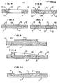
- Fig. 4 illustrates a holder formed as a ring 30 with an exterior extended lip 31 and an inner recessed shoulder 32 which supports a wafer 33.
- the wafer 33 is supported so that its upper surface is in the plane of the upper surface of the holder 30.
- the lip 31 is of suitable thickness and shape to mate with the shoulder 18 of the electrode 12 so as to support the ring 30 in any one of the apertures 15, 15a or 15b in electrode 12 so that the upper surface of the ring 30 is in the plane of the surface of the electrode 12.
- each of the holders shown in Figs. 4, 5, 6, and 7 could be modified so that the lip extends above the surface of the plane of the electrode.
- Fig. 8 shows a mesa type holder.
- This holder comprises a central body 51 provided with an extended lip 52 which rests on the shoulder 18 in the electrode 12.
- the body 51 is of such a thickness that it extends above the plane of the upper surface of the electrode 12 as a mesa and thus supports the wafer 53 above the plane of the upper surface of the electrode 12.
- Fig. 9 shows a holder that comprises a recessed dish 61 provided with an exterior rim 62 and a central recess 63 into which a wafer 64 can be inserted.
- the central recess 63 is provided with a flat bottom parallel to the upper surface of the electrode 12.
- the lip 62 is provided with an upwardly extending rim of variable thickness.
- Fig. 10 shows a variation of the beveled holder of Fig. 9.
- the wafer holder 65 is provided with an extended lip 66 and a central recess 67 into which a wafer 69 can be inserted.
- the central recess 67 has a flat bottom 68 set at an angle with respect to the upper surface of the electrode 12.
- the lip 62 is provided with a rim of variable thickness. Again by varying the thickness of the rim from one side of the holder to the other, the plane of the upper surface of the rim is again at an angle with the plane of the upper surface of the electrode 12.
- the bottom of the recess 67 is maintained at the same angle as the plane of the upper surface of the rim 66 with respect to the surface of the electrode 12 and slightly below the surface of the rim.
- Wafer uniformity means that uniformity measured using 5 points per wafer and with the result published as 3 sigma/x information.
- the holder design of Fig. 6 is used to solve both effects 1 and 2 above.
- Another added feature of the design shown in Fig. 6 is, by decreasing the depth of the recess 43 the wafer 44 the etch rate across the whole wafer is increased slightly and by deepening the recess, the etch rate of the wafer is decreased.
- the wafer is not recessed but instead is raised above the surface of the electrode by the mesa configured holder, as shown in Fig. 8, the outside edge of the wafer 53 will etch faster. With this knowledge one can populate an entire electrode with holders having different depths of recess or different height of mesa for improved batch uniformity.
- the holder design of Fig. 7 can especially be used to improve center etch rates due to better RF coupling in this region, this corrects effect number 2.
- the holder design of Fig. 5 is used to increase etch rate on the outer edge of the wafer due to better RF coupling, thus curing effect number 1.
- Both of these holder designs are susceptible to heat transfer problems. The areas of the wafer not contacting the thermally conductive pedestal tend to heat up during the etch causing some films to etch at different rates. This can be corrected by adding a heat transfer medium, which insulates electrically, to these areas of the wafer.
- the holder designs shown in Fig. 9 and 10 are best used to correct effects number 3 and number 4 above. Usually these effects are brought on by effects from the electrode edge. These edge effects generally cause the portion of the wafer closest to the electrode edge to etch faster than the remainder of the wafer.
- the rim of the pedestal is raised higher on one side than the other, usually about 0.89 cm, one can compensate for the edge effect.
- the holder is preferably positioned in the electrode so that the high side of the rim will be closest to the outermost electrode edge, thereby protecting the outside edge of the wafer more.
- the holder design, shown in Fig. 9, keeps the wafer surface parallel with the electrode surface.
- RIE reactive ion etching
- the holders can either be coated with or formed of an insulating material to improve uniformity of the etching of.the wafer.
- a holder of volatile substance chosen so that it etches at the same rate as the wafer film assists in correcting effect number 2 described above.
- this invention teaches that by using an apertured electrode and placing in the apertures product holders of selected designs that uniform etching of the product can be realized regardless of the product position in the apparatus.
- each holder controls the etching uniformity of the product contained therein by altering the local physical characteristics immediately surrounding the product contained in the holder.
- the local characteristics around each product is modified according to its own particular needs by suitable design of the holder.
Abstract
Description
- The present invention relates generally to plasma etching apparatus and more particularly to an improved plasma etching apparatus electrode structure.
- Plasma etching techniques have been widely used for etching products such as semiconductor wafers. Basically such a technique comprises the exposing of wafers to a plasma to remove surface materials, such as silicon oxide, carried on the semiconductor wafer surface. These plasma etching techniques are used in the semiconductor industry because the plasma etching process involves low temperatures. Low temperatures are realized because the power required to generate the plasma is low. Because the process uses low temperatures the use of photoresist as a mask material is permitted. Also, because plasma etching is fundamentally a chemical process, selectivity in etching is very high and mask erosion can be made minimal.
- The difficulty with such etching is non-uniformity of the species forming the plasma with respect to the material being treated. This is caused, in part by electrical field variations between the cathode and the anode.
- Traditionally the products to be etched, such as wafers, are batch etched, that is they are evenly spaced upon one electrode of the plasma etching machine and exposed to the plasma. Because large numbers of wafers can be treated at once in such batch etchers they are the preferred production etching tool even though the poor uniformity realized in such tools requires considerable tradeoffs in device size, tolerances, etc. Although such batch etching increases the throughput it has been found that because of the gas flow, temperature, electric fields, plasma formation, etc. in the usual apparatus the plasma affects each wafer, in the batch, differently depending on its location in the apparatus. Thus the rate of and amount of etching realized by each wafer depends significantly on the wafers position on the electrode. In general, the etching rate varies with the radial position of the wafer on the electrode. Thus batch etched wafers are non-uniformly etched.
- This problem of non-uniformity has been addressed in the past by; selectively spacing the wafers from the electrode with quartz spacers; providing extension shields around the entire electrode in an attempt to even out the dark space over the electrode (see the -article "Ground Shield in RF Sputter Etching" by Y. Budo i.a. published in the IBM Technical Disclosure Bulletin, Vol. 13, No. 5, 10-1970, p. 1296); curving the electrode surface (see US-Patent 4,297,162) and by altering the distribution of the plasma forming gas flow within the apparatus (see US-Patents 4,230,515 and 4,307,283).
- Even with these solutions, in the prior art considerable etching uniformity problems were encountered and batch uniformity was found to range 18 % to 25 % with the central wafers etching faster than the wafers positioned around the edges of the electrode.
- Thus the solutions discussed above did not provide significant improvements to the etching uniformity problem and until the present invention the best uniformity between wafers was achieved only when each wafer was etched individually, for example, in a single wafer etcher. Such single wafer etchers have a very low throughput and therefore are expensive to use and have such a low output that their use as a production tool is economically discouraged.
- It is the object of the invention to provide a plasma etching apparatus in which any product placed therein can be etched at substantially the same rate regardless of its position within the plasma etching apparatus, in which uniformity of etching across the surface of any individual wafer regardless of its size is assured and in which etching variations due to the differences in the films deposited on the product being treated in the etching apparatus can be compensated.
- This object is achieved by a plasma etching apparatus as defined in claim 1.
- With the inventive batch plasma etching apparatus having a unique electrode a heretofore unattainable etching uniformity can be achieved - by compensating for the plasma field or chamber abnormalities - while reaching the high throughput of the batch etchers.
- This significant improvement in etching uniformity is realized by inserting into apertures of the wafer carrying electrode tailored product holders. Each such holder is tailored, with respect to its geographic location on the electrode, so that the characteristics of the plasma, immediately surrounding each product contained in the holder, is modified to be substantially identical to that surrounding any other product contained in any other holder. Furthermore, each holder can be tailored to compensate not only for the differences in its geographical location on the electrode but can be tailored to compensate for film abnormalities such as film thickness differences that may be on the surface of the product in the holder. Individual treatment of each of the wafers to be etched can be provided.
- Advantageous embodiments of the inventive apparatus are defined in the subclaims.
- The invention will become further apparent from the following description taken in conjunction with the drawings.
-
- Fig. 1 is a cross sectional view of a batch plasma etching apparatus.
- Fig. 2 is a top view of the electrode of the apparatus of Fig. 1 formed according to the present invention.
- Fig. 3 shows an enlarged, partial, sectional view of the electrode of Fig. 2 taken along the lines 3-3.
- Figs. 4, 5, all show cross sectional views of 6, 7, 8, 9 various wafer holders for use with and 10 the electrode of Fig. 2.
- The present invention solves the uniformity problems encountered in the past by forming the electrode of the apparatus with a plurality of apertures into which a plurality of product holders can be inserted. It should be understood that depending on the apparatus, biasing, etc. the electrode can be either the anode or the cathode of the apparatus. These holders assure both good electrical and thermal contact to the product contained therein but are also designed to physically modify the characteristics of the plasma within the vicinity of the holder. The holder configuration can also be altered to take into consideration the type of film being removed as well as the geographic location of the holders within the reactor.
- As shown in Fig. 1 a cross sectional view of a typical batch type, parallel plasma etcher is shown. Basically such plasma etchers comprise a
chamber 10 containing an upper electrode 11, and alower electrode 12 which is carrying a plurality ofsemiconductor wafers 13. In the configuration shown, electrode 11 is the cathode andelectrode 12 is the anode and both are coupled to an R-F source (not shown). A plasma forming gas is introduced via tube 14 through the center of cathode 11 into thechamber 10 and between theelectrodes 11 and 12. With such a gas in the chamber 11 a plasma is formed between theelectrodes 11 and 12 when the RF source is turned on. Plasma forming gas is extracted from thechamber 10 via outlet tube 9 which is coupled to a vacuum pump;(not shown). Such etching apparatus is presently commercially available and need not be further discussed. - It should be noted that although Fig. 1 shows a chamber with a top gas inlet and a bottom outlet that side inlet and outlet chambers can also be used.
- The
anode 12 of Fig. 1, designed in accordance with the present invention, is shown in greater detail in Figs. 2 and 3. In Fig. 2 a top view of the anode is shown. This anode typically, when designed for use with semiconductor wafers about 9.53 cm in diameter, comprises a substantially flat circular plate, about 0.64 cm in thickness, having a diameter of about 66.04 cm. - It should, of course be understood that the diameter and thickness of such electrodes will vary depending on the machine in which they are to be used and with the diameters of the wafers to be treated. Such variations and modifications are, of course, well within the art and need not be further explained here.
- For the sake of convenience of description herein however, it will be assumed that only 3.25 inch semiconductor wafers are being used.
- In accordance with the present invention the
electrode 12, as shown in Fig. 2, has a plurality of apertures therein. These apertures are arranged in arrays, usually as a series of concentric rings. In the electrode shown, acentral aperture 15 is surrounded by two concentric rings ofapertures 15a and 15b respectively. All of these apertures are identical to one another and each has a stepped inner wall as especially shown in Fig. 3. Thelarger diameter 16 of the aperture is approximately 9.53 cm while thesmaller diameter 17 is about 8.26 cm. Thus a 0.64cm shoulder 18 is provided for in each aperture. - Different wafer holders suitable for insertion in the electrode of Fig. 2, are shown in Figs. 4 through 8.
- Fig. 4 illustrates a holder formed as a
ring 30 with an exterior extendedlip 31 and an innerrecessed shoulder 32 which supports awafer 33. Thewafer 33 is supported so that its upper surface is in the plane of the upper surface of theholder 30. Thelip 31 is of suitable thickness and shape to mate with theshoulder 18 of theelectrode 12 so as to support thering 30 in any one of theapertures electrode 12 so that the upper surface of thering 30 is in the plane of the surface of theelectrode 12. -
- Fig. 5 illustrates another wafer holder. In this instance the holder comprises a
ring 35 formed with an extended lip 36 and provided with an innerrecessed shoulder 37 into which awafer 38 can be set. The lip 36 and therecessed shoulder 37 are of sufficient thickness and depth respectively to assure that the upper surfaces of thering 35, thewafer 38 and theelectrode 12 are all in the same plane. The bottom central interior of thering 35 is filled in with aninsert 39 which extends from the bottom of thering 35 to a level below that of thewafer 38 so that aspace 40, approximately equal to the thickness of thewafer 38 is left between the bottom of thewafer 38 and the upper surface of theinsert 39. This insert can be either conductive or insulating although a conductive insert is usually preferred. - Fig. 6 shows a wafer holder formed as a recessed dish 41 having an
extended lip 42 and acentral recess 43. Again the thickness of the lip is such that the top of the holder is in the plane of theelectrode 12. The depth of therecess 43 is at least twice the thickness of thewafer 44 which is placed therein so that it rests on the bottom of the dish thus the surface of thewafer 44 sits in the dish and is beneath the plane of theelectrode 12 when the holder is placed in theelectrode 12. - Fig. 7 shows a holder that is quite similar to the holder shown in Fig. 6 and comprises a recessed
dish 45 having anextended lip 46, and acentral recess 47, whose depth is twice the thickness of thewafer 48, placed therein. In addition therecess 47 is provided with agroove 49 encircling its outer edge so that acentral pedestal 50 is created in the center of the dish. Thisgroove 49 should preferably have a depth at least equal to the thickness of the wafer. This causes the outer edge of thewafer 48 is cantilevered from thecentral pedestal 50. - It should be noted that each of the holders shown in Figs. 4, 5, 6, and 7 could be modified so that the lip extends above the surface of the plane of the electrode.
- Fig. 8 shows a mesa type holder. This holder comprises a
central body 51 provided with anextended lip 52 which rests on theshoulder 18 in theelectrode 12. In this figure thebody 51 is of such a thickness that it extends above the plane of the upper surface of theelectrode 12 as a mesa and thus supports thewafer 53 above the plane of the upper surface of theelectrode 12. - Fig. 9 shows a holder that comprises a recessed dish 61 provided with an
exterior rim 62 and acentral recess 63 into which awafer 64 can be inserted. Thecentral recess 63 is provided with a flat bottom parallel to the upper surface of theelectrode 12. Thelip 62 is provided with an upwardly extending rim of variable thickness. By varying the thickness of the rim from one side of the holder to the other the plane of the upper surface of therim 62 is at an angle to the plane of the upper surface of theelectrode 12, thus therim 62, on one side, extends above the upper surface of theelectrode 12 while on the other side is substantially at the same level as the surface of theelectrode 12. - Fig. 10 shows a variation of the beveled holder of Fig. 9. Here the
wafer holder 65 is provided with anextended lip 66 and acentral recess 67 into which awafer 69 can be inserted. Thecentral recess 67 has a flat bottom 68 set at an angle with respect to the upper surface of theelectrode 12. Again thelip 62 is provided with a rim of variable thickness. Again by varying the thickness of the rim from one side of the holder to the other, the plane of the upper surface of the rim is again at an angle with the plane of the upper surface of theelectrode 12. Preferably, the bottom of therecess 67 is maintained at the same angle as the plane of the upper surface of therim 66 with respect to the surface of theelectrode 12 and slightly below the surface of the rim. - Initially, samples were run using electrodes loaded with each of the different shaped wafer holders shown in Fig. 4 thru 7. With a plasma tool operating at 1275 watts, a gas flow of 90 sccm, 100 % 02 at 60 millitorr at 20°C, and a photo resist and polyimide coating on each wafer in each holder the average, within wafer uniformity, for electrodes loaded with each type of wafer holder shown in Figs. 4, 5, 6 and 7 is set forth below.
- The average within wafer uniformity for an electrode loaded with the holder shown in Fig. 4 was 13.1 %. Wafer uniformity as used herein means that uniformity measured using 5 points per wafer and with the result published as 3 sigma/x information.
- When the holders were changed to the shape shown in Fig. 5 the within wafer uniformity was improved to 12.1 %.
- The substitution of the holder shown in Fig. 6 resulted in still a further improvement in uniformity of to 9.7 %. Holders as shown in Fig. 7 did not appreciably change the result and a wafer uniformity of 10 % was achieved. Because the holder shown in Fig. 6 resulted in the lowest within wafer uniformity, this was chosen for further tests.
- When the holder, shown in Fig. 6, was employed it was found that the within wafer-uniformity on the inner central positions, 15 and 15a of Fig. 1, was 10 % or less but at the outer positions, 15b of Fig. 1, the wafer uniformity averaged 15.8 %. This indicated that wafers in the outer positions 15b were being etched at a faster rate than those wafers placed in the
inner positions inner positions - These differences in etching uniformity can better be understood from the following discussion. Generally these fall into four categories, which are:
- 1) Center area of the wafer etching faster than the outer edge.
- 2) Outer edge of the wafer etching faster than the center area.
- 3) A portion of the outside edge etching faster than the remainder of the wafer.
- 4) The areas of the electrode near the electrode edges etching faster than the remainder of the electrode.
- Combinations of these effects can also occur. To combat these maladies the basic wafer holder designs set out in Fig. 4 to 10 are used.
- The holder design of Fig. 6 is used to solve both effects 1 and 2 above. The deeper the
recess 43 the slower the outside edge of thewafer 44 etches, due to protection by thelip 42. Another added feature of the design shown in Fig. 6 is, by decreasing the depth of therecess 43 thewafer 44 the etch rate across the whole wafer is increased slightly and by deepening the recess, the etch rate of the wafer is decreased. Alternately if the wafer is not recessed but instead is raised above the surface of the electrode by the mesa configured holder, as shown in Fig. 8, the outside edge of thewafer 53 will etch faster. With this knowledge one can populate an entire electrode with holders having different depths of recess or different height of mesa for improved batch uniformity. - The holder design of Fig. 7 can especially be used to improve center etch rates due to better RF coupling in this region, this corrects effect number 2. The holder design of Fig. 5 is used to increase etch rate on the outer edge of the wafer due to better RF coupling, thus curing effect number 1. Both of these holder designs are susceptible to heat transfer problems. The areas of the wafer not contacting the thermally conductive pedestal tend to heat up during the etch causing some films to etch at different rates. This can be corrected by adding a heat transfer medium, which insulates electrically, to these areas of the wafer.
- The holder designs shown in Fig. 9 and 10 are best used to correct
effects number 3 and number 4 above. Usually these effects are brought on by effects from the electrode edge. These edge effects generally cause the portion of the wafer closest to the electrode edge to etch faster than the remainder of the wafer. By using the design of Fig. 9, in which the rim of the pedestal is raised higher on one side than the other, usually about 0.89 cm, one can compensate for the edge effect. The holder is preferably positioned in the electrode so that the high side of the rim will be closest to the outermost electrode edge, thereby protecting the outside edge of the wafer more. The holder design, shown in Fig. 9, keeps the wafer surface parallel with the electrode surface. As noted the modified design of Fig. 10 actually tilts the wafer with respect to the surface ofelectrode 12. There are basic differences in plasma etching and reactive ion etching (RIE). RIE is a directional etch while plasma etching is generally not. Therefore in order to have sidewalls etched straight down in RIE one must have the wafer parallel to the electrode surface, i. e., the design as shown in Fig. 9. However plasma etching being non-directional allows the wafer to be tilted so that the raised area of the wafer, as shown in Fig. 10, can be positioned closer to the upper electrode and etched to a greater extent. By using either the design shown in Fig. 9 or Fig. 10 one can effectively cancel the edge effects found on the outermost ring of apertures onelectrode 12 and procure the best results regardless of the type of etching being performed. - It should be understood that another factor to be considered in creating an electrode with an optimum holder is to consider the material from which the holder is to be formed, for the material can alter the RF field and affect the desired effects. For example, the holders can either be coated with or formed of an insulating material to improve uniformity of the etching of.the wafer. Thus by surrounding the wafer with a holder of volatile substance, chosen so that it etches at the same rate as the wafer film assists in correcting effect number 2 described above.
- Thus this invention teaches that by using an apertured electrode and placing in the apertures product holders of selected designs that uniform etching of the product can be realized regardless of the product position in the apparatus.
- This occurs because each holder controls the etching uniformity of the product contained therein by altering the local physical characteristics immediately surrounding the product contained in the holder. The local characteristics around each product is modified according to its own particular needs by suitable design of the holder. These individual holders significantly improve uniformity of product etching on the anode by compensating for both film and reactor chamber abnormalities by physically affecting the local RF field.
- Although a batch etcher has been described in detail it should be noted that the modification of the holder, as taught herein, could be used in a single wafer etcher.
- It should also be understood that although a flat batch electrode was shown that a curved electrode could also be used but that the shape of holders may require some modification to compensate for the curve of the electrode.
Claims (11)
Applications Claiming Priority (2)
| Application Number | Priority Date | Filing Date | Title |
|---|---|---|---|
| US596189 | 1984-04-02 | ||
| US06/596,189 US4512841A (en) | 1984-04-02 | 1984-04-02 | RF Coupling techniques |
Publications (3)
| Publication Number | Publication Date |
|---|---|
| EP0160220A1 true EP0160220A1 (en) | 1985-11-06 |
| EP0160220B1 EP0160220B1 (en) | 1989-05-31 |
| EP0160220B2 EP0160220B2 (en) | 1992-08-19 |
Family
ID=24386313
Family Applications (1)
| Application Number | Title | Priority Date | Filing Date |
|---|---|---|---|
| EP85103878A Expired EP0160220B2 (en) | 1984-04-02 | 1985-03-31 | Plasma etching apparatus |
Country Status (4)
| Country | Link |
|---|---|
| US (1) | US4512841A (en) |
| EP (1) | EP0160220B2 (en) |
| JP (1) | JPS60208836A (en) |
| DE (1) | DE3570805D1 (en) |
Cited By (4)
| Publication number | Priority date | Publication date | Assignee | Title |
|---|---|---|---|---|
| US6051503A (en) * | 1996-08-01 | 2000-04-18 | Surface Technology Systems Limited | Method of surface treatment of semiconductor substrates |
| US6187685B1 (en) | 1997-08-01 | 2001-02-13 | Surface Technology Systems Limited | Method and apparatus for etching a substrate |
| US6261962B1 (en) | 1996-08-01 | 2001-07-17 | Surface Technology Systems Limited | Method of surface treatment of semiconductor substrates |
| US6417013B1 (en) | 1999-01-29 | 2002-07-09 | Plasma-Therm, Inc. | Morphed processing of semiconductor devices |
Families Citing this family (258)
| Publication number | Priority date | Publication date | Assignee | Title |
|---|---|---|---|---|
| US4647361A (en) * | 1985-09-03 | 1987-03-03 | International Business Machines Corporation | Sputtering apparatus |
| JPH01200629A (en) * | 1988-02-04 | 1989-08-11 | Nec Corp | Dry etching apparatus |
| US5262029A (en) * | 1988-05-23 | 1993-11-16 | Lam Research | Method and system for clamping semiconductor wafers |
| US5511799A (en) | 1993-06-07 | 1996-04-30 | Applied Materials, Inc. | Sealing device useful in semiconductor processing apparatus for bridging materials having a thermal expansion differential |
| GB9317170D0 (en) * | 1993-08-18 | 1993-10-06 | Applied Vision Ltd | Improvements in physical vapour deposition apparatus |
| US5498313A (en) * | 1993-08-20 | 1996-03-12 | International Business Machines Corp. | Symmetrical etching ring with gas control |
| JPH08153682A (en) * | 1994-11-29 | 1996-06-11 | Nec Corp | Plasma cvd device |
| US5639334A (en) * | 1995-03-07 | 1997-06-17 | International Business Machines Corporation | Uniform gas flow arrangements |
| JP2001230235A (en) * | 2000-02-14 | 2001-08-24 | Matsushita Electric Ind Co Ltd | Plasma etching device for crystal plate and method for manufacturing crystal plate as well as crystal plate |
| JP2004193632A (en) * | 2004-03-22 | 2004-07-08 | Matsushita Electric Ind Co Ltd | Plasma etching device for quartz plate |
| DE102004053906A1 (en) * | 2004-11-05 | 2006-05-11 | Leica Microsystems Semiconductor Gmbh | Adapter device for a substrate workstation |
| US7419551B2 (en) * | 2006-05-03 | 2008-09-02 | Applied Materials, Inc. | Plasma reactor with apparatus for dynamically adjusting the plasma source power applicator and the workpiece relative to one another |
| US7504041B2 (en) * | 2006-05-03 | 2009-03-17 | Applied Materials, Inc. | Method of processing a workpiece in a plasma reactor employing a dynamically adjustable plasma source power applicator |
| US7520999B2 (en) * | 2006-05-03 | 2009-04-21 | Applied Materials, Inc. | Method of processing a workpiece in a plasma reactor with dynamic adjustment of the plasma source power applicator and the workpiece relative to one another |
| US7431797B2 (en) * | 2006-05-03 | 2008-10-07 | Applied Materials, Inc. | Plasma reactor with a dynamically adjustable plasma source power applicator |
| US8557093B2 (en) | 2007-03-22 | 2013-10-15 | Sunpower Corporation | Deposition system with electrically isolated pallet and anode assemblies |
| DE102007023970A1 (en) * | 2007-05-23 | 2008-12-04 | Aixtron Ag | Apparatus for coating a plurality of densely packed substrates on a susceptor |
| US8962101B2 (en) | 2007-08-31 | 2015-02-24 | Novellus Systems, Inc. | Methods and apparatus for plasma-based deposition |
| JP5094307B2 (en) * | 2007-09-25 | 2012-12-12 | 株式会社アルバック | Plasma processing equipment |
| US8062472B2 (en) * | 2007-12-19 | 2011-11-22 | Applied Materials, Inc. | Method of correcting baseline skew by a novel motorized source coil assembly |
| US8137463B2 (en) * | 2007-12-19 | 2012-03-20 | Applied Materials, Inc. | Dual zone gas injection nozzle |
| US8999106B2 (en) * | 2007-12-19 | 2015-04-07 | Applied Materials, Inc. | Apparatus and method for controlling edge performance in an inductively coupled plasma chamber |
| US20090162570A1 (en) * | 2007-12-19 | 2009-06-25 | Applied Materials, Inc. | Apparatus and method for processing a substrate using inductively coupled plasma technology |
| US20100055318A1 (en) * | 2008-08-29 | 2010-03-04 | Veeco Instruments Inc. | Wafer carrier with varying thermal resistance |
| US9394608B2 (en) | 2009-04-06 | 2016-07-19 | Asm America, Inc. | Semiconductor processing reactor and components thereof |
| EP2539920A1 (en) * | 2010-02-24 | 2013-01-02 | Veeco Instruments Inc. | Processing methods and apparatus with temperature distribution control |
| TWI452163B (en) * | 2010-04-08 | 2014-09-11 | Hon Hai Prec Ind Co Ltd | Plating apparatus |
| US8535445B2 (en) * | 2010-08-13 | 2013-09-17 | Veeco Instruments Inc. | Enhanced wafer carrier |
| TWI450330B (en) * | 2010-11-25 | 2014-08-21 | C Sun Mfg Ltd | Plasma etching equipment, wafer jig and method for disposing wafers |
| US20120164834A1 (en) * | 2010-12-22 | 2012-06-28 | Kevin Jennings | Variable-Density Plasma Processing of Semiconductor Substrates |
| US20130023129A1 (en) | 2011-07-20 | 2013-01-24 | Asm America, Inc. | Pressure transmitter for a semiconductor processing environment |
| DE102011055061A1 (en) | 2011-11-04 | 2013-05-08 | Aixtron Se | CVD reactor or substrate holder for a CVD reactor |
| KR101928356B1 (en) * | 2012-02-16 | 2018-12-12 | 엘지이노텍 주식회사 | Apparatus for manufacturing semiconductor |
| US10316412B2 (en) | 2012-04-18 | 2019-06-11 | Veeco Instruments Inc. | Wafter carrier for chemical vapor deposition systems |
| US9088085B2 (en) | 2012-09-21 | 2015-07-21 | Novellus Systems, Inc. | High temperature electrode connections |
| US10714315B2 (en) | 2012-10-12 | 2020-07-14 | Asm Ip Holdings B.V. | Semiconductor reaction chamber showerhead |
| US9273413B2 (en) | 2013-03-14 | 2016-03-01 | Veeco Instruments Inc. | Wafer carrier with temperature distribution control |
| US10167571B2 (en) | 2013-03-15 | 2019-01-01 | Veeco Instruments Inc. | Wafer carrier having provisions for improving heating uniformity in chemical vapor deposition systems |
| US11015245B2 (en) | 2014-03-19 | 2021-05-25 | Asm Ip Holding B.V. | Gas-phase reactor and system having exhaust plenum and components thereof |
| US10858737B2 (en) | 2014-07-28 | 2020-12-08 | Asm Ip Holding B.V. | Showerhead assembly and components thereof |
| US10941490B2 (en) | 2014-10-07 | 2021-03-09 | Asm Ip Holding B.V. | Multiple temperature range susceptor, assembly, reactor and system including the susceptor, and methods of using the same |
| JP6567667B2 (en) * | 2014-11-26 | 2019-08-28 | フォン アルデンヌ アセット ゲーエムベーハー ウント コー カーゲー | Substrate holding device, substrate transport device, processing arrangement, and method for processing a substrate |
| US10276355B2 (en) | 2015-03-12 | 2019-04-30 | Asm Ip Holding B.V. | Multi-zone reactor, system including the reactor, and method of using the same |
| US10458018B2 (en) | 2015-06-26 | 2019-10-29 | Asm Ip Holding B.V. | Structures including metal carbide material, devices including the structures, and methods of forming same |
| US10211308B2 (en) | 2015-10-21 | 2019-02-19 | Asm Ip Holding B.V. | NbMC layers |
| US11139308B2 (en) | 2015-12-29 | 2021-10-05 | Asm Ip Holding B.V. | Atomic layer deposition of III-V compounds to form V-NAND devices |
| US10529554B2 (en) | 2016-02-19 | 2020-01-07 | Asm Ip Holding B.V. | Method for forming silicon nitride film selectively on sidewalls or flat surfaces of trenches |
| US10190213B2 (en) | 2016-04-21 | 2019-01-29 | Asm Ip Holding B.V. | Deposition of metal borides |
| US10367080B2 (en) | 2016-05-02 | 2019-07-30 | Asm Ip Holding B.V. | Method of forming a germanium oxynitride film |
| US11453943B2 (en) | 2016-05-25 | 2022-09-27 | Asm Ip Holding B.V. | Method for forming carbon-containing silicon/metal oxide or nitride film by ALD using silicon precursor and hydrocarbon precursor |
| US9859151B1 (en) | 2016-07-08 | 2018-01-02 | Asm Ip Holding B.V. | Selective film deposition method to form air gaps |
| US10612137B2 (en) | 2016-07-08 | 2020-04-07 | Asm Ip Holdings B.V. | Organic reactants for atomic layer deposition |
| US9812320B1 (en) | 2016-07-28 | 2017-11-07 | Asm Ip Holding B.V. | Method and apparatus for filling a gap |
| US9887082B1 (en) | 2016-07-28 | 2018-02-06 | Asm Ip Holding B.V. | Method and apparatus for filling a gap |
| KR102532607B1 (en) | 2016-07-28 | 2023-05-15 | 에이에스엠 아이피 홀딩 비.브이. | Substrate processing apparatus and method of operating the same |
| US10643826B2 (en) | 2016-10-26 | 2020-05-05 | Asm Ip Holdings B.V. | Methods for thermally calibrating reaction chambers |
| US11532757B2 (en) | 2016-10-27 | 2022-12-20 | Asm Ip Holding B.V. | Deposition of charge trapping layers |
| US10714350B2 (en) | 2016-11-01 | 2020-07-14 | ASM IP Holdings, B.V. | Methods for forming a transition metal niobium nitride film on a substrate by atomic layer deposition and related semiconductor device structures |
| KR102546317B1 (en) | 2016-11-15 | 2023-06-21 | 에이에스엠 아이피 홀딩 비.브이. | Gas supply unit and substrate processing apparatus including the same |
| KR20180068582A (en) | 2016-12-14 | 2018-06-22 | 에이에스엠 아이피 홀딩 비.브이. | Substrate processing apparatus |
| US11447861B2 (en) | 2016-12-15 | 2022-09-20 | Asm Ip Holding B.V. | Sequential infiltration synthesis apparatus and a method of forming a patterned structure |
| US11581186B2 (en) | 2016-12-15 | 2023-02-14 | Asm Ip Holding B.V. | Sequential infiltration synthesis apparatus |
| KR20180070971A (en) | 2016-12-19 | 2018-06-27 | 에이에스엠 아이피 홀딩 비.브이. | Substrate processing apparatus |
| US10269558B2 (en) | 2016-12-22 | 2019-04-23 | Asm Ip Holding B.V. | Method of forming a structure on a substrate |
| US10867788B2 (en) | 2016-12-28 | 2020-12-15 | Asm Ip Holding B.V. | Method of forming a structure on a substrate |
| US11390950B2 (en) | 2017-01-10 | 2022-07-19 | Asm Ip Holding B.V. | Reactor system and method to reduce residue buildup during a film deposition process |
| US10468261B2 (en) | 2017-02-15 | 2019-11-05 | Asm Ip Holding B.V. | Methods for forming a metallic film on a substrate by cyclical deposition and related semiconductor device structures |
| US10529563B2 (en) | 2017-03-29 | 2020-01-07 | Asm Ip Holdings B.V. | Method for forming doped metal oxide films on a substrate by cyclical deposition and related semiconductor device structures |
| KR102457289B1 (en) | 2017-04-25 | 2022-10-21 | 에이에스엠 아이피 홀딩 비.브이. | Method for depositing a thin film and manufacturing a semiconductor device |
| US10892156B2 (en) | 2017-05-08 | 2021-01-12 | Asm Ip Holding B.V. | Methods for forming a silicon nitride film on a substrate and related semiconductor device structures |
| US10770286B2 (en) | 2017-05-08 | 2020-09-08 | Asm Ip Holdings B.V. | Methods for selectively forming a silicon nitride film on a substrate and related semiconductor device structures |
| KR102417931B1 (en) * | 2017-05-30 | 2022-07-06 | 에이에스엠 아이피 홀딩 비.브이. | Substrate supporting device and substrate processing apparatus including the same |
| US10886123B2 (en) | 2017-06-02 | 2021-01-05 | Asm Ip Holding B.V. | Methods for forming low temperature semiconductor layers and related semiconductor device structures |
| US11306395B2 (en) | 2017-06-28 | 2022-04-19 | Asm Ip Holding B.V. | Methods for depositing a transition metal nitride film on a substrate by atomic layer deposition and related deposition apparatus |
| KR20190009245A (en) | 2017-07-18 | 2019-01-28 | 에이에스엠 아이피 홀딩 비.브이. | Methods for forming a semiconductor device structure and related semiconductor device structures |
| US11374112B2 (en) | 2017-07-19 | 2022-06-28 | Asm Ip Holding B.V. | Method for depositing a group IV semiconductor and related semiconductor device structures |
| US10541333B2 (en) | 2017-07-19 | 2020-01-21 | Asm Ip Holding B.V. | Method for depositing a group IV semiconductor and related semiconductor device structures |
| US11018002B2 (en) | 2017-07-19 | 2021-05-25 | Asm Ip Holding B.V. | Method for selectively depositing a Group IV semiconductor and related semiconductor device structures |
| US10590535B2 (en) | 2017-07-26 | 2020-03-17 | Asm Ip Holdings B.V. | Chemical treatment, deposition and/or infiltration apparatus and method for using the same |
| US10692741B2 (en) | 2017-08-08 | 2020-06-23 | Asm Ip Holdings B.V. | Radiation shield |
| US10770336B2 (en) | 2017-08-08 | 2020-09-08 | Asm Ip Holding B.V. | Substrate lift mechanism and reactor including same |
| US11769682B2 (en) | 2017-08-09 | 2023-09-26 | Asm Ip Holding B.V. | Storage apparatus for storing cassettes for substrates and processing apparatus equipped therewith |
| US11139191B2 (en) | 2017-08-09 | 2021-10-05 | Asm Ip Holding B.V. | Storage apparatus for storing cassettes for substrates and processing apparatus equipped therewith |
| US11830730B2 (en) | 2017-08-29 | 2023-11-28 | Asm Ip Holding B.V. | Layer forming method and apparatus |
| KR102491945B1 (en) | 2017-08-30 | 2023-01-26 | 에이에스엠 아이피 홀딩 비.브이. | Substrate processing apparatus |
| US11056344B2 (en) | 2017-08-30 | 2021-07-06 | Asm Ip Holding B.V. | Layer forming method |
| US11295980B2 (en) | 2017-08-30 | 2022-04-05 | Asm Ip Holding B.V. | Methods for depositing a molybdenum metal film over a dielectric surface of a substrate by a cyclical deposition process and related semiconductor device structures |
| KR102630301B1 (en) | 2017-09-21 | 2024-01-29 | 에이에스엠 아이피 홀딩 비.브이. | Method of sequential infiltration synthesis treatment of infiltrateable material and structures and devices formed using same |
| US10844484B2 (en) | 2017-09-22 | 2020-11-24 | Asm Ip Holding B.V. | Apparatus for dispensing a vapor phase reactant to a reaction chamber and related methods |
| US10658205B2 (en) | 2017-09-28 | 2020-05-19 | Asm Ip Holdings B.V. | Chemical dispensing apparatus and methods for dispensing a chemical to a reaction chamber |
| US10403504B2 (en) | 2017-10-05 | 2019-09-03 | Asm Ip Holding B.V. | Method for selectively depositing a metallic film on a substrate |
| US10923344B2 (en) | 2017-10-30 | 2021-02-16 | Asm Ip Holding B.V. | Methods for forming a semiconductor structure and related semiconductor structures |
| US10910262B2 (en) | 2017-11-16 | 2021-02-02 | Asm Ip Holding B.V. | Method of selectively depositing a capping layer structure on a semiconductor device structure |
| US11022879B2 (en) | 2017-11-24 | 2021-06-01 | Asm Ip Holding B.V. | Method of forming an enhanced unexposed photoresist layer |
| JP7206265B2 (en) | 2017-11-27 | 2023-01-17 | エーエスエム アイピー ホールディング ビー.ブイ. | Equipment with a clean mini-environment |
| CN111316417B (en) | 2017-11-27 | 2023-12-22 | 阿斯莫Ip控股公司 | Storage device for storing wafer cassettes for use with batch ovens |
| US10872771B2 (en) | 2018-01-16 | 2020-12-22 | Asm Ip Holding B. V. | Method for depositing a material film on a substrate within a reaction chamber by a cyclical deposition process and related device structures |
| CN111630203A (en) | 2018-01-19 | 2020-09-04 | Asm Ip私人控股有限公司 | Method for depositing gap filling layer by plasma auxiliary deposition |
| TW202325889A (en) | 2018-01-19 | 2023-07-01 | 荷蘭商Asm 智慧財產控股公司 | Deposition method |
| US11018047B2 (en) | 2018-01-25 | 2021-05-25 | Asm Ip Holding B.V. | Hybrid lift pin |
| USD880437S1 (en) | 2018-02-01 | 2020-04-07 | Asm Ip Holding B.V. | Gas supply plate for semiconductor manufacturing apparatus |
| US11081345B2 (en) | 2018-02-06 | 2021-08-03 | Asm Ip Holding B.V. | Method of post-deposition treatment for silicon oxide film |
| WO2019158960A1 (en) | 2018-02-14 | 2019-08-22 | Asm Ip Holding B.V. | A method for depositing a ruthenium-containing film on a substrate by a cyclical deposition process |
| US10896820B2 (en) | 2018-02-14 | 2021-01-19 | Asm Ip Holding B.V. | Method for depositing a ruthenium-containing film on a substrate by a cyclical deposition process |
| KR102636427B1 (en) | 2018-02-20 | 2024-02-13 | 에이에스엠 아이피 홀딩 비.브이. | Substrate processing method and apparatus |
| US10975470B2 (en) | 2018-02-23 | 2021-04-13 | Asm Ip Holding B.V. | Apparatus for detecting or monitoring for a chemical precursor in a high temperature environment |
| US11473195B2 (en) | 2018-03-01 | 2022-10-18 | Asm Ip Holding B.V. | Semiconductor processing apparatus and a method for processing a substrate |
| US11629406B2 (en) | 2018-03-09 | 2023-04-18 | Asm Ip Holding B.V. | Semiconductor processing apparatus comprising one or more pyrometers for measuring a temperature of a substrate during transfer of the substrate |
| US11114283B2 (en) | 2018-03-16 | 2021-09-07 | Asm Ip Holding B.V. | Reactor, system including the reactor, and methods of manufacturing and using same |
| KR102646467B1 (en) | 2018-03-27 | 2024-03-11 | 에이에스엠 아이피 홀딩 비.브이. | Method of forming an electrode on a substrate and a semiconductor device structure including an electrode |
| US11088002B2 (en) | 2018-03-29 | 2021-08-10 | Asm Ip Holding B.V. | Substrate rack and a substrate processing system and method |
| US11230766B2 (en) | 2018-03-29 | 2022-01-25 | Asm Ip Holding B.V. | Substrate processing apparatus and method |
| KR102501472B1 (en) | 2018-03-30 | 2023-02-20 | 에이에스엠 아이피 홀딩 비.브이. | Substrate processing method |
| KR20190128558A (en) | 2018-05-08 | 2019-11-18 | 에이에스엠 아이피 홀딩 비.브이. | Methods for depositing an oxide film on a substrate by a cyclical deposition process and related device structures |
| TW202349473A (en) | 2018-05-11 | 2023-12-16 | 荷蘭商Asm Ip私人控股有限公司 | Methods for forming a doped metal carbide film on a substrate and related semiconductor device structures |
| KR102596988B1 (en) | 2018-05-28 | 2023-10-31 | 에이에스엠 아이피 홀딩 비.브이. | Method of processing a substrate and a device manufactured by the same |
| TW202013553A (en) | 2018-06-04 | 2020-04-01 | 荷蘭商Asm 智慧財產控股公司 | Wafer handling chamber with moisture reduction |
| US11718913B2 (en) | 2018-06-04 | 2023-08-08 | Asm Ip Holding B.V. | Gas distribution system and reactor system including same |
| US11286562B2 (en) | 2018-06-08 | 2022-03-29 | Asm Ip Holding B.V. | Gas-phase chemical reactor and method of using same |
| US10797133B2 (en) | 2018-06-21 | 2020-10-06 | Asm Ip Holding B.V. | Method for depositing a phosphorus doped silicon arsenide film and related semiconductor device structures |
| KR102568797B1 (en) | 2018-06-21 | 2023-08-21 | 에이에스엠 아이피 홀딩 비.브이. | Substrate processing system |
| WO2020003000A1 (en) | 2018-06-27 | 2020-01-02 | Asm Ip Holding B.V. | Cyclic deposition methods for forming metal-containing material and films and structures including the metal-containing material |
| CN112292478A (en) | 2018-06-27 | 2021-01-29 | Asm Ip私人控股有限公司 | Cyclic deposition methods for forming metal-containing materials and films and structures containing metal-containing materials |
| US10612136B2 (en) | 2018-06-29 | 2020-04-07 | ASM IP Holding, B.V. | Temperature-controlled flange and reactor system including same |
| KR20200002519A (en) | 2018-06-29 | 2020-01-08 | 에이에스엠 아이피 홀딩 비.브이. | Method for depositing a thin film and manufacturing a semiconductor device |
| US10755922B2 (en) | 2018-07-03 | 2020-08-25 | Asm Ip Holding B.V. | Method for depositing silicon-free carbon-containing film as gap-fill layer by pulse plasma-assisted deposition |
| US10388513B1 (en) | 2018-07-03 | 2019-08-20 | Asm Ip Holding B.V. | Method for depositing silicon-free carbon-containing film as gap-fill layer by pulse plasma-assisted deposition |
| US11053591B2 (en) | 2018-08-06 | 2021-07-06 | Asm Ip Holding B.V. | Multi-port gas injection system and reactor system including same |
| US10883175B2 (en) | 2018-08-09 | 2021-01-05 | Asm Ip Holding B.V. | Vertical furnace for processing substrates and a liner for use therein |
| US11430674B2 (en) | 2018-08-22 | 2022-08-30 | Asm Ip Holding B.V. | Sensor array, apparatus for dispensing a vapor phase reactant to a reaction chamber and related methods |
| KR20200030162A (en) | 2018-09-11 | 2020-03-20 | 에이에스엠 아이피 홀딩 비.브이. | Method for deposition of a thin film |
| US11024523B2 (en) | 2018-09-11 | 2021-06-01 | Asm Ip Holding B.V. | Substrate processing apparatus and method |
| US11049751B2 (en) | 2018-09-14 | 2021-06-29 | Asm Ip Holding B.V. | Cassette supply system to store and handle cassettes and processing apparatus equipped therewith |
| CN110970344A (en) | 2018-10-01 | 2020-04-07 | Asm Ip控股有限公司 | Substrate holding apparatus, system including the same, and method of using the same |
| US11232963B2 (en) | 2018-10-03 | 2022-01-25 | Asm Ip Holding B.V. | Substrate processing apparatus and method |
| KR102592699B1 (en) | 2018-10-08 | 2023-10-23 | 에이에스엠 아이피 홀딩 비.브이. | Substrate support unit and apparatuses for depositing thin film and processing the substrate including the same |
| KR102605121B1 (en) | 2018-10-19 | 2023-11-23 | 에이에스엠 아이피 홀딩 비.브이. | Substrate processing apparatus and substrate processing method |
| KR102546322B1 (en) | 2018-10-19 | 2023-06-21 | 에이에스엠 아이피 홀딩 비.브이. | Substrate processing apparatus and substrate processing method |
| USD948463S1 (en) | 2018-10-24 | 2022-04-12 | Asm Ip Holding B.V. | Susceptor for semiconductor substrate supporting apparatus |
| US11087997B2 (en) | 2018-10-31 | 2021-08-10 | Asm Ip Holding B.V. | Substrate processing apparatus for processing substrates |
| KR20200051105A (en) | 2018-11-02 | 2020-05-13 | 에이에스엠 아이피 홀딩 비.브이. | Substrate support unit and substrate processing apparatus including the same |
| US11572620B2 (en) | 2018-11-06 | 2023-02-07 | Asm Ip Holding B.V. | Methods for selectively depositing an amorphous silicon film on a substrate |
| US11031242B2 (en) | 2018-11-07 | 2021-06-08 | Asm Ip Holding B.V. | Methods for depositing a boron doped silicon germanium film |
| US10847366B2 (en) | 2018-11-16 | 2020-11-24 | Asm Ip Holding B.V. | Methods for depositing a transition metal chalcogenide film on a substrate by a cyclical deposition process |
| US10818758B2 (en) | 2018-11-16 | 2020-10-27 | Asm Ip Holding B.V. | Methods for forming a metal silicate film on a substrate in a reaction chamber and related semiconductor device structures |
| US11217444B2 (en) | 2018-11-30 | 2022-01-04 | Asm Ip Holding B.V. | Method for forming an ultraviolet radiation responsive metal oxide-containing film |
| KR102636428B1 (en) | 2018-12-04 | 2024-02-13 | 에이에스엠 아이피 홀딩 비.브이. | A method for cleaning a substrate processing apparatus |
| US11158513B2 (en) | 2018-12-13 | 2021-10-26 | Asm Ip Holding B.V. | Methods for forming a rhenium-containing film on a substrate by a cyclical deposition process and related semiconductor device structures |
| TW202037745A (en) | 2018-12-14 | 2020-10-16 | 荷蘭商Asm Ip私人控股有限公司 | Method of forming device structure, structure formed by the method and system for performing the method |
| TWI819180B (en) | 2019-01-17 | 2023-10-21 | 荷蘭商Asm 智慧財產控股公司 | Methods of forming a transition metal containing film on a substrate by a cyclical deposition process |
| KR20200091543A (en) | 2019-01-22 | 2020-07-31 | 에이에스엠 아이피 홀딩 비.브이. | Semiconductor processing device |
| CN111524788B (en) | 2019-02-01 | 2023-11-24 | Asm Ip私人控股有限公司 | Method for topologically selective film formation of silicon oxide |
| KR102626263B1 (en) | 2019-02-20 | 2024-01-16 | 에이에스엠 아이피 홀딩 비.브이. | Cyclical deposition method including treatment step and apparatus for same |
| US11482533B2 (en) | 2019-02-20 | 2022-10-25 | Asm Ip Holding B.V. | Apparatus and methods for plug fill deposition in 3-D NAND applications |
| TW202104632A (en) | 2019-02-20 | 2021-02-01 | 荷蘭商Asm Ip私人控股有限公司 | Cyclical deposition method and apparatus for filling a recess formed within a substrate surface |
| JP2020136678A (en) | 2019-02-20 | 2020-08-31 | エーエスエム・アイピー・ホールディング・ベー・フェー | Method for filing concave part formed inside front surface of base material, and device |
| TW202100794A (en) | 2019-02-22 | 2021-01-01 | 荷蘭商Asm Ip私人控股有限公司 | Substrate processing apparatus and method for processing substrate |
| KR20200108243A (en) | 2019-03-08 | 2020-09-17 | 에이에스엠 아이피 홀딩 비.브이. | Structure Including SiOC Layer and Method of Forming Same |
| US11742198B2 (en) | 2019-03-08 | 2023-08-29 | Asm Ip Holding B.V. | Structure including SiOCN layer and method of forming same |
| KR20200108242A (en) | 2019-03-08 | 2020-09-17 | 에이에스엠 아이피 홀딩 비.브이. | Method for Selective Deposition of Silicon Nitride Layer and Structure Including Selectively-Deposited Silicon Nitride Layer |
| JP2020167398A (en) | 2019-03-28 | 2020-10-08 | エーエスエム・アイピー・ホールディング・ベー・フェー | Door opener and substrate processing apparatus provided therewith |
| KR20200116855A (en) | 2019-04-01 | 2020-10-13 | 에이에스엠 아이피 홀딩 비.브이. | Method of manufacturing semiconductor device |
| KR20200123380A (en) | 2019-04-19 | 2020-10-29 | 에이에스엠 아이피 홀딩 비.브이. | Layer forming method and apparatus |
| KR20200125453A (en) | 2019-04-24 | 2020-11-04 | 에이에스엠 아이피 홀딩 비.브이. | Gas-phase reactor system and method of using same |
| KR20200130121A (en) | 2019-05-07 | 2020-11-18 | 에이에스엠 아이피 홀딩 비.브이. | Chemical source vessel with dip tube |
| KR20200130118A (en) | 2019-05-07 | 2020-11-18 | 에이에스엠 아이피 홀딩 비.브이. | Method for Reforming Amorphous Carbon Polymer Film |
| KR20200130652A (en) | 2019-05-10 | 2020-11-19 | 에이에스엠 아이피 홀딩 비.브이. | Method of depositing material onto a surface and structure formed according to the method |
| JP2020188255A (en) | 2019-05-16 | 2020-11-19 | エーエスエム アイピー ホールディング ビー.ブイ. | Wafer boat handling device, vertical batch furnace, and method |
| USD947913S1 (en) | 2019-05-17 | 2022-04-05 | Asm Ip Holding B.V. | Susceptor shaft |
| USD975665S1 (en) | 2019-05-17 | 2023-01-17 | Asm Ip Holding B.V. | Susceptor shaft |
| USD935572S1 (en) | 2019-05-24 | 2021-11-09 | Asm Ip Holding B.V. | Gas channel plate |
| USD922229S1 (en) | 2019-06-05 | 2021-06-15 | Asm Ip Holding B.V. | Device for controlling a temperature of a gas supply unit |
| KR20200141002A (en) | 2019-06-06 | 2020-12-17 | 에이에스엠 아이피 홀딩 비.브이. | Method of using a gas-phase reactor system including analyzing exhausted gas |
| KR20200143254A (en) | 2019-06-11 | 2020-12-23 | 에이에스엠 아이피 홀딩 비.브이. | Method of forming an electronic structure using an reforming gas, system for performing the method, and structure formed using the method |
| USD944946S1 (en) | 2019-06-14 | 2022-03-01 | Asm Ip Holding B.V. | Shower plate |
| USD931978S1 (en) | 2019-06-27 | 2021-09-28 | Asm Ip Holding B.V. | Showerhead vacuum transport |
| KR20210005515A (en) | 2019-07-03 | 2021-01-14 | 에이에스엠 아이피 홀딩 비.브이. | Temperature control assembly for substrate processing apparatus and method of using same |
| JP2021015791A (en) | 2019-07-09 | 2021-02-12 | エーエスエム アイピー ホールディング ビー.ブイ. | Plasma device and substrate processing method using coaxial waveguide |
| CN112216646A (en) | 2019-07-10 | 2021-01-12 | Asm Ip私人控股有限公司 | Substrate supporting assembly and substrate processing device comprising same |
| KR20210010307A (en) | 2019-07-16 | 2021-01-27 | 에이에스엠 아이피 홀딩 비.브이. | Substrate processing apparatus |
| KR20210010816A (en) | 2019-07-17 | 2021-01-28 | 에이에스엠 아이피 홀딩 비.브이. | Radical assist ignition plasma system and method |
| KR20210010820A (en) | 2019-07-17 | 2021-01-28 | 에이에스엠 아이피 홀딩 비.브이. | Methods of forming silicon germanium structures |
| US11643724B2 (en) | 2019-07-18 | 2023-05-09 | Asm Ip Holding B.V. | Method of forming structures using a neutral beam |
| TW202121506A (en) | 2019-07-19 | 2021-06-01 | 荷蘭商Asm Ip私人控股有限公司 | Method of forming topology-controlled amorphous carbon polymer film |
| CN112309843A (en) | 2019-07-29 | 2021-02-02 | Asm Ip私人控股有限公司 | Selective deposition method for achieving high dopant doping |
| CN112309899A (en) | 2019-07-30 | 2021-02-02 | Asm Ip私人控股有限公司 | Substrate processing apparatus |
| CN112309900A (en) | 2019-07-30 | 2021-02-02 | Asm Ip私人控股有限公司 | Substrate processing apparatus |
| US11587815B2 (en) | 2019-07-31 | 2023-02-21 | Asm Ip Holding B.V. | Vertical batch furnace assembly |
| US11587814B2 (en) | 2019-07-31 | 2023-02-21 | Asm Ip Holding B.V. | Vertical batch furnace assembly |
| US11227782B2 (en) | 2019-07-31 | 2022-01-18 | Asm Ip Holding B.V. | Vertical batch furnace assembly |
| CN112323048B (en) | 2019-08-05 | 2024-02-09 | Asm Ip私人控股有限公司 | Liquid level sensor for chemical source container |
| USD965044S1 (en) | 2019-08-19 | 2022-09-27 | Asm Ip Holding B.V. | Susceptor shaft |
| USD965524S1 (en) | 2019-08-19 | 2022-10-04 | Asm Ip Holding B.V. | Susceptor support |
| JP2021031769A (en) | 2019-08-21 | 2021-03-01 | エーエスエム アイピー ホールディング ビー.ブイ. | Production apparatus of mixed gas of film deposition raw material and film deposition apparatus |
| USD930782S1 (en) | 2019-08-22 | 2021-09-14 | Asm Ip Holding B.V. | Gas distributor |
| USD979506S1 (en) | 2019-08-22 | 2023-02-28 | Asm Ip Holding B.V. | Insulator |
| USD949319S1 (en) | 2019-08-22 | 2022-04-19 | Asm Ip Holding B.V. | Exhaust duct |
| KR20210024423A (en) | 2019-08-22 | 2021-03-05 | 에이에스엠 아이피 홀딩 비.브이. | Method for forming a structure with a hole |
| USD940837S1 (en) | 2019-08-22 | 2022-01-11 | Asm Ip Holding B.V. | Electrode |
| KR20210024420A (en) | 2019-08-23 | 2021-03-05 | 에이에스엠 아이피 홀딩 비.브이. | Method for depositing silicon oxide film having improved quality by peald using bis(diethylamino)silane |
| US11286558B2 (en) | 2019-08-23 | 2022-03-29 | Asm Ip Holding B.V. | Methods for depositing a molybdenum nitride film on a surface of a substrate by a cyclical deposition process and related semiconductor device structures including a molybdenum nitride film |
| KR20210029090A (en) | 2019-09-04 | 2021-03-15 | 에이에스엠 아이피 홀딩 비.브이. | Methods for selective deposition using a sacrificial capping layer |
| KR20210029663A (en) | 2019-09-05 | 2021-03-16 | 에이에스엠 아이피 홀딩 비.브이. | Substrate processing apparatus |
| US11562901B2 (en) | 2019-09-25 | 2023-01-24 | Asm Ip Holding B.V. | Substrate processing method |
| CN112593212B (en) | 2019-10-02 | 2023-12-22 | Asm Ip私人控股有限公司 | Method for forming topologically selective silicon oxide film by cyclic plasma enhanced deposition process |
| TW202129060A (en) | 2019-10-08 | 2021-08-01 | 荷蘭商Asm Ip控股公司 | Substrate processing device, and substrate processing method |
| TW202115273A (en) | 2019-10-10 | 2021-04-16 | 荷蘭商Asm Ip私人控股有限公司 | Method of forming a photoresist underlayer and structure including same |
| KR20210045930A (en) | 2019-10-16 | 2021-04-27 | 에이에스엠 아이피 홀딩 비.브이. | Method of Topology-Selective Film Formation of Silicon Oxide |
| US11637014B2 (en) | 2019-10-17 | 2023-04-25 | Asm Ip Holding B.V. | Methods for selective deposition of doped semiconductor material |
| KR20210047808A (en) | 2019-10-21 | 2021-04-30 | 에이에스엠 아이피 홀딩 비.브이. | Apparatus and methods for selectively etching films |
| US11646205B2 (en) | 2019-10-29 | 2023-05-09 | Asm Ip Holding B.V. | Methods of selectively forming n-type doped material on a surface, systems for selectively forming n-type doped material, and structures formed using same |
| KR20210054983A (en) | 2019-11-05 | 2021-05-14 | 에이에스엠 아이피 홀딩 비.브이. | Structures with doped semiconductor layers and methods and systems for forming same |
| US11501968B2 (en) | 2019-11-15 | 2022-11-15 | Asm Ip Holding B.V. | Method for providing a semiconductor device with silicon filled gaps |
| KR20210062561A (en) | 2019-11-20 | 2021-05-31 | 에이에스엠 아이피 홀딩 비.브이. | Method of depositing carbon-containing material on a surface of a substrate, structure formed using the method, and system for forming the structure |
| CN112951697A (en) | 2019-11-26 | 2021-06-11 | Asm Ip私人控股有限公司 | Substrate processing apparatus |
| KR20210065848A (en) | 2019-11-26 | 2021-06-04 | 에이에스엠 아이피 홀딩 비.브이. | Methods for selectivley forming a target film on a substrate comprising a first dielectric surface and a second metallic surface |
| CN112885692A (en) | 2019-11-29 | 2021-06-01 | Asm Ip私人控股有限公司 | Substrate processing apparatus |
| CN112885693A (en) | 2019-11-29 | 2021-06-01 | Asm Ip私人控股有限公司 | Substrate processing apparatus |
| JP2021090042A (en) | 2019-12-02 | 2021-06-10 | エーエスエム アイピー ホールディング ビー.ブイ. | Substrate processing apparatus and substrate processing method |
| KR20210070898A (en) | 2019-12-04 | 2021-06-15 | 에이에스엠 아이피 홀딩 비.브이. | Substrate processing apparatus |
| KR20210078405A (en) | 2019-12-17 | 2021-06-28 | 에이에스엠 아이피 홀딩 비.브이. | Method of forming vanadium nitride layer and structure including the vanadium nitride layer |
| US11527403B2 (en) | 2019-12-19 | 2022-12-13 | Asm Ip Holding B.V. | Methods for filling a gap feature on a substrate surface and related semiconductor structures |
| KR20210095050A (en) | 2020-01-20 | 2021-07-30 | 에이에스엠 아이피 홀딩 비.브이. | Method of forming thin film and method of modifying surface of thin film |
| TW202130846A (en) | 2020-02-03 | 2021-08-16 | 荷蘭商Asm Ip私人控股有限公司 | Method of forming structures including a vanadium or indium layer |
| TW202146882A (en) | 2020-02-04 | 2021-12-16 | 荷蘭商Asm Ip私人控股有限公司 | Method of verifying an article, apparatus for verifying an article, and system for verifying a reaction chamber |
| US11776846B2 (en) | 2020-02-07 | 2023-10-03 | Asm Ip Holding B.V. | Methods for depositing gap filling fluids and related systems and devices |
| TW202146715A (en) | 2020-02-17 | 2021-12-16 | 荷蘭商Asm Ip私人控股有限公司 | Method for growing phosphorous-doped silicon layer and system of the same |
| US11876356B2 (en) | 2020-03-11 | 2024-01-16 | Asm Ip Holding B.V. | Lockout tagout assembly and system and method of using same |
| KR20210116240A (en) | 2020-03-11 | 2021-09-27 | 에이에스엠 아이피 홀딩 비.브이. | Substrate handling device with adjustable joints |
| KR20210124042A (en) | 2020-04-02 | 2021-10-14 | 에이에스엠 아이피 홀딩 비.브이. | Thin film forming method |
| TW202146689A (en) | 2020-04-03 | 2021-12-16 | 荷蘭商Asm Ip控股公司 | Method for forming barrier layer and method for manufacturing semiconductor device |
| TW202145344A (en) | 2020-04-08 | 2021-12-01 | 荷蘭商Asm Ip私人控股有限公司 | Apparatus and methods for selectively etching silcon oxide films |
| US11821078B2 (en) | 2020-04-15 | 2023-11-21 | Asm Ip Holding B.V. | Method for forming precoat film and method for forming silicon-containing film |
| US11898243B2 (en) | 2020-04-24 | 2024-02-13 | Asm Ip Holding B.V. | Method of forming vanadium nitride-containing layer |
| KR20210132605A (en) | 2020-04-24 | 2021-11-04 | 에이에스엠 아이피 홀딩 비.브이. | Vertical batch furnace assembly comprising a cooling gas supply |
| KR20210132600A (en) | 2020-04-24 | 2021-11-04 | 에이에스엠 아이피 홀딩 비.브이. | Methods and systems for depositing a layer comprising vanadium, nitrogen, and a further element |
| KR20210134869A (en) | 2020-05-01 | 2021-11-11 | 에이에스엠 아이피 홀딩 비.브이. | Fast FOUP swapping with a FOUP handler |
| KR20210141379A (en) | 2020-05-13 | 2021-11-23 | 에이에스엠 아이피 홀딩 비.브이. | Laser alignment fixture for a reactor system |
| KR20210143653A (en) | 2020-05-19 | 2021-11-29 | 에이에스엠 아이피 홀딩 비.브이. | Substrate processing apparatus |
| KR20210145078A (en) | 2020-05-21 | 2021-12-01 | 에이에스엠 아이피 홀딩 비.브이. | Structures including multiple carbon layers and methods of forming and using same |
| TW202201602A (en) | 2020-05-29 | 2022-01-01 | 荷蘭商Asm Ip私人控股有限公司 | Substrate processing device |
| TW202218133A (en) | 2020-06-24 | 2022-05-01 | 荷蘭商Asm Ip私人控股有限公司 | Method for forming a layer provided with silicon |
| TW202217953A (en) | 2020-06-30 | 2022-05-01 | 荷蘭商Asm Ip私人控股有限公司 | Substrate processing method |
| KR20220010438A (en) | 2020-07-17 | 2022-01-25 | 에이에스엠 아이피 홀딩 비.브이. | Structures and methods for use in photolithography |
| TW202204662A (en) | 2020-07-20 | 2022-02-01 | 荷蘭商Asm Ip私人控股有限公司 | Method and system for depositing molybdenum layers |
| TW202212623A (en) | 2020-08-26 | 2022-04-01 | 荷蘭商Asm Ip私人控股有限公司 | Method of forming metal silicon oxide layer and metal silicon oxynitride layer, semiconductor structure, and system |
| USD990534S1 (en) | 2020-09-11 | 2023-06-27 | Asm Ip Holding B.V. | Weighted lift pin |
| USD1012873S1 (en) | 2020-09-24 | 2024-01-30 | Asm Ip Holding B.V. | Electrode for semiconductor processing apparatus |
| TW202229613A (en) | 2020-10-14 | 2022-08-01 | 荷蘭商Asm Ip私人控股有限公司 | Method of depositing material on stepped structure |
| TW202217037A (en) | 2020-10-22 | 2022-05-01 | 荷蘭商Asm Ip私人控股有限公司 | Method of depositing vanadium metal, structure, device and a deposition assembly |
| TW202223136A (en) | 2020-10-28 | 2022-06-16 | 荷蘭商Asm Ip私人控股有限公司 | Method for forming layer on substrate, and semiconductor processing system |
| TW202235675A (en) | 2020-11-30 | 2022-09-16 | 荷蘭商Asm Ip私人控股有限公司 | Injector, and substrate processing apparatus |
| US11946137B2 (en) | 2020-12-16 | 2024-04-02 | Asm Ip Holding B.V. | Runout and wobble measurement fixtures |
| TW202231903A (en) | 2020-12-22 | 2022-08-16 | 荷蘭商Asm Ip私人控股有限公司 | Transition metal deposition method, transition metal layer, and deposition assembly for depositing transition metal on substrate |
| USD980813S1 (en) | 2021-05-11 | 2023-03-14 | Asm Ip Holding B.V. | Gas flow control plate for substrate processing apparatus |
| USD980814S1 (en) | 2021-05-11 | 2023-03-14 | Asm Ip Holding B.V. | Gas distributor for substrate processing apparatus |
| USD981973S1 (en) | 2021-05-11 | 2023-03-28 | Asm Ip Holding B.V. | Reactor wall for substrate processing apparatus |
| USD990441S1 (en) | 2021-09-07 | 2023-06-27 | Asm Ip Holding B.V. | Gas flow control plate |
Citations (6)
| Publication number | Priority date | Publication date | Assignee | Title |
|---|---|---|---|---|
| US3436255A (en) * | 1965-07-06 | 1969-04-01 | Monsanto Co | Electric resistance heaters |
| EP0045057A1 (en) * | 1980-07-28 | 1982-02-03 | Siemens Aktiengesellschaft | Apparatus for holding disc-shaped substrates |
| US4350578A (en) * | 1981-05-11 | 1982-09-21 | International Business Machines Corporation | Cathode for etching |
| US4399016A (en) * | 1981-03-12 | 1983-08-16 | Anelva Corporation | Plasma device comprising an intermediate electrode out of contact with a high frequency electrode to induce electrostatic attraction |
| US4400235A (en) * | 1982-03-25 | 1983-08-23 | Bell Telephone Laboratories, Incorporated | Etching apparatus and method |
| GB2124958A (en) * | 1982-07-26 | 1984-02-29 | Western Electric Co | Plasma-assisted etching process |
Family Cites Families (7)
| Publication number | Priority date | Publication date | Assignee | Title |
|---|---|---|---|---|
| US4230515A (en) * | 1978-07-27 | 1980-10-28 | Davis & Wilder, Inc. | Plasma etching apparatus |
| US4222839A (en) * | 1978-09-21 | 1980-09-16 | Motorola, Inc. | Workpiece holder and method for plasma reactor apparatus |
| US4298443A (en) * | 1979-08-09 | 1981-11-03 | Bell Telephone Laboratories, Incorporated | High capacity etching apparatus and method |
| US4307283A (en) * | 1979-09-27 | 1981-12-22 | Eaton Corporation | Plasma etching apparatus II-conical-shaped projection |
| US4297162A (en) * | 1979-10-17 | 1981-10-27 | Texas Instruments Incorporated | Plasma etching using improved electrode |
| US4309267A (en) * | 1980-07-21 | 1982-01-05 | Bell Telephone Laboratories, Incorporated | Reactive sputter etching apparatus |
| US4439261A (en) * | 1983-08-26 | 1984-03-27 | International Business Machines Corporation | Composite pallet |
-
1984
- 1984-04-02 US US06/596,189 patent/US4512841A/en not_active Expired - Fee Related
-
1985
- 1985-01-31 JP JP60015635A patent/JPS60208836A/en active Granted
- 1985-03-31 EP EP85103878A patent/EP0160220B2/en not_active Expired
- 1985-03-31 DE DE8585103878T patent/DE3570805D1/en not_active Expired
Patent Citations (6)
| Publication number | Priority date | Publication date | Assignee | Title |
|---|---|---|---|---|
| US3436255A (en) * | 1965-07-06 | 1969-04-01 | Monsanto Co | Electric resistance heaters |
| EP0045057A1 (en) * | 1980-07-28 | 1982-02-03 | Siemens Aktiengesellschaft | Apparatus for holding disc-shaped substrates |
| US4399016A (en) * | 1981-03-12 | 1983-08-16 | Anelva Corporation | Plasma device comprising an intermediate electrode out of contact with a high frequency electrode to induce electrostatic attraction |
| US4350578A (en) * | 1981-05-11 | 1982-09-21 | International Business Machines Corporation | Cathode for etching |
| US4400235A (en) * | 1982-03-25 | 1983-08-23 | Bell Telephone Laboratories, Incorporated | Etching apparatus and method |
| GB2124958A (en) * | 1982-07-26 | 1984-02-29 | Western Electric Co | Plasma-assisted etching process |
Non-Patent Citations (2)
| Title |
|---|
| IBM TECHNICAL DISCLOSURE BULLETIN, vol. 20, no. 7, December 1977, New York GARTNER et al. "Achieving Uniform Etch Rates in Reactive Ion Plasma Etching Processes" page 2703 * Last paragraph * * |
| SOLID STATE TECHNOLOGY, December 1975, Port Washington TISONE: "Low Voltage Triode Sputtering with a Confined Plasma" pages 34-40 * Page 36 ; fig. 5 ; left column, last 8 lines * * |
Cited By (4)
| Publication number | Priority date | Publication date | Assignee | Title |
|---|---|---|---|---|
| US6051503A (en) * | 1996-08-01 | 2000-04-18 | Surface Technology Systems Limited | Method of surface treatment of semiconductor substrates |
| US6261962B1 (en) | 1996-08-01 | 2001-07-17 | Surface Technology Systems Limited | Method of surface treatment of semiconductor substrates |
| US6187685B1 (en) | 1997-08-01 | 2001-02-13 | Surface Technology Systems Limited | Method and apparatus for etching a substrate |
| US6417013B1 (en) | 1999-01-29 | 2002-07-09 | Plasma-Therm, Inc. | Morphed processing of semiconductor devices |
Also Published As
| Publication number | Publication date |
|---|---|
| EP0160220B2 (en) | 1992-08-19 |
| JPS60208836A (en) | 1985-10-21 |
| DE3570805D1 (en) | 1989-07-06 |
| EP0160220B1 (en) | 1989-05-31 |
| JPH0476493B2 (en) | 1992-12-03 |
| US4512841A (en) | 1985-04-23 |
Similar Documents
| Publication | Publication Date | Title |
|---|---|---|
| EP0160220B2 (en) | Plasma etching apparatus | |
| KR101008863B1 (en) | Plasma apparatus with device for reducing polymer deposition on a substrate and method for reducing polymer deposition | |
| US4600464A (en) | Plasma etching reactor with reduced plasma potential | |
| US6733620B1 (en) | Process apparatus | |
| KR100322416B1 (en) | Plasma processing unit using texture focusing | |
| EP0165400B1 (en) | Apparatus for plasma etching | |
| US5022979A (en) | Electrode for use in the treatment of an object in a plasma | |
| US6689249B2 (en) | Shield or ring surrounding semiconductor workpiece in plasma chamber | |
| US5498313A (en) | Symmetrical etching ring with gas control | |
| US20050078953A1 (en) | Substrate heater assembly | |
| KR20040111691A (en) | Multi-part electrode for a semiconductor processing plasma reactor and method of replacing a portion of a multi-part electrode | |
| EP0047395B1 (en) | System for reactive ion etching | |
| KR20010032700A (en) | A processing chamber and method for confining plasma | |
| WO1999014788A1 (en) | Shield or ring surrounding semiconductor workpiece in plasma chamber | |
| US4810322A (en) | Anode plate for a parallel-plate reactive ion etching reactor | |
| US5789324A (en) | Uniform gas flow arrangements | |
| US5480052A (en) | Domed extension for process chamber electrode | |
| JPH04196319A (en) | Discharge treatment device | |
| JP2734908B2 (en) | Plasma processing equipment | |
| CN213583695U (en) | Plasma processing device | |
| JPH0760816B2 (en) | Dry etching equipment | |
| JPH0766174A (en) | Plasma etching tool |
Legal Events
| Date | Code | Title | Description |
|---|---|---|---|
| PUAI | Public reference made under article 153(3) epc to a published international application that has entered the european phase |
Free format text: ORIGINAL CODE: 0009012 |
|
| AK | Designated contracting states |
Designated state(s): DE FR GB IT |
|
| 17P | Request for examination filed |
Effective date: 19860225 |
|
| 17Q | First examination report despatched |
Effective date: 19871222 |
|
| GRAA | (expected) grant |
Free format text: ORIGINAL CODE: 0009210 |
|
| AK | Designated contracting states |
Kind code of ref document: B1 Designated state(s): DE FR GB IT |
|
| REF | Corresponds to: |
Ref document number: 3570805 Country of ref document: DE Date of ref document: 19890706 |
|
| ET | Fr: translation filed | ||
| ITF | It: translation for a ep patent filed |
Owner name: IBM - DR. ALFREDO BRAVI |
|
| PLBI | Opposition filed |
Free format text: ORIGINAL CODE: 0009260 |
|
| 26 | Opposition filed |
Opponent name: LEYBOLD AKTIENGESELLSCHAFT Effective date: 19891116 |
|
| ITTA | It: last paid annual fee | ||
| PUAH | Patent maintained in amended form |
Free format text: ORIGINAL CODE: 0009272 |
|
| STAA | Information on the status of an ep patent application or granted ep patent |
Free format text: STATUS: PATENT MAINTAINED AS AMENDED |
|
| 27A | Patent maintained in amended form |
Effective date: 19920819 |
|
| AK | Designated contracting states |
Kind code of ref document: B2 Designated state(s): DE FR GB IT |
|
| ET3 | Fr: translation filed ** decision concerning opposition | ||
| PGFP | Annual fee paid to national office [announced via postgrant information from national office to epo] |
Ref country code: FR Payment date: 19950228 Year of fee payment: 11 |
|
| PGFP | Annual fee paid to national office [announced via postgrant information from national office to epo] |
Ref country code: GB Payment date: 19960311 Year of fee payment: 12 |
|
| PGFP | Annual fee paid to national office [announced via postgrant information from national office to epo] |
Ref country code: DE Payment date: 19960313 Year of fee payment: 12 |
|
| PG25 | Lapsed in a contracting state [announced via postgrant information from national office to epo] |
Ref country code: FR Effective date: 19961129 |
|
| REG | Reference to a national code |
Ref country code: FR Ref legal event code: ST |
|
| PG25 | Lapsed in a contracting state [announced via postgrant information from national office to epo] |
Ref country code: GB Effective date: 19970331 |
|
| GBPC | Gb: european patent ceased through non-payment of renewal fee |
Effective date: 19970331 |
|
| PG25 | Lapsed in a contracting state [announced via postgrant information from national office to epo] |
Ref country code: DE Effective date: 19971202 |