EP0158122A2 - Programmier-Stecker - Google Patents
Programmier-Stecker Download PDFInfo
- Publication number
- EP0158122A2 EP0158122A2 EP85102598A EP85102598A EP0158122A2 EP 0158122 A2 EP0158122 A2 EP 0158122A2 EP 85102598 A EP85102598 A EP 85102598A EP 85102598 A EP85102598 A EP 85102598A EP 0158122 A2 EP0158122 A2 EP 0158122A2
- Authority
- EP
- European Patent Office
- Prior art keywords
- contacts
- contact
- sockets
- component carrier
- short
- Prior art date
- Legal status (The legal status is an assumption and is not a legal conclusion. Google has not performed a legal analysis and makes no representation as to the accuracy of the status listed.)
- Granted
Links
Images
Classifications
-
- H—ELECTRICITY
- H01—ELECTRIC ELEMENTS
- H01R—ELECTRICALLY-CONDUCTIVE CONNECTIONS; STRUCTURAL ASSOCIATIONS OF A PLURALITY OF MUTUALLY-INSULATED ELECTRICAL CONNECTING ELEMENTS; COUPLING DEVICES; CURRENT COLLECTORS
- H01R29/00—Coupling parts for selective co-operation with a counterpart in different ways to establish different circuits, e.g. for voltage selection, for series-parallel selection, programmable connectors
-
- H—ELECTRICITY
- H01—ELECTRIC ELEMENTS
- H01H—ELECTRIC SWITCHES; RELAYS; SELECTORS; EMERGENCY PROTECTIVE DEVICES
- H01H15/00—Switches having rectilinearly-movable operating part or parts adapted for actuation in opposite directions, e.g. slide switch
- H01H15/005—Switches having rectilinearly-movable operating part or parts adapted for actuation in opposite directions, e.g. slide switch adapted for connection with printed circuit boards
-
- H—ELECTRICITY
- H01—ELECTRIC ELEMENTS
- H01R—ELECTRICALLY-CONDUCTIVE CONNECTIONS; STRUCTURAL ASSOCIATIONS OF A PLURALITY OF MUTUALLY-INSULATED ELECTRICAL CONNECTING ELEMENTS; COUPLING DEVICES; CURRENT COLLECTORS
- H01R12/00—Structural associations of a plurality of mutually-insulated electrical connecting elements, specially adapted for printed circuits, e.g. printed circuit boards [PCB], flat or ribbon cables, or like generally planar structures, e.g. terminal strips, terminal blocks; Coupling devices specially adapted for printed circuits, flat or ribbon cables, or like generally planar structures; Terminals specially adapted for contact with, or insertion into, printed circuits, flat or ribbon cables, or like generally planar structures
- H01R12/70—Coupling devices
- H01R12/7005—Guiding, mounting, polarizing or locking means; Extractors
- H01R12/7011—Locking or fixing a connector to a PCB
- H01R12/707—Soldering or welding
-
- H—ELECTRICITY
- H01—ELECTRIC ELEMENTS
- H01R—ELECTRICALLY-CONDUCTIVE CONNECTIONS; STRUCTURAL ASSOCIATIONS OF A PLURALITY OF MUTUALLY-INSULATED ELECTRICAL CONNECTING ELEMENTS; COUPLING DEVICES; CURRENT COLLECTORS
- H01R12/00—Structural associations of a plurality of mutually-insulated electrical connecting elements, specially adapted for printed circuits, e.g. printed circuit boards [PCB], flat or ribbon cables, or like generally planar structures, e.g. terminal strips, terminal blocks; Coupling devices specially adapted for printed circuits, flat or ribbon cables, or like generally planar structures; Terminals specially adapted for contact with, or insertion into, printed circuits, flat or ribbon cables, or like generally planar structures
- H01R12/70—Coupling devices
- H01R12/71—Coupling devices for rigid printing circuits or like structures
- H01R12/712—Coupling devices for rigid printing circuits or like structures co-operating with the surface of the printed circuit or with a coupling device exclusively provided on the surface of the printed circuit
-
- H—ELECTRICITY
- H01—ELECTRIC ELEMENTS
- H01R—ELECTRICALLY-CONDUCTIVE CONNECTIONS; STRUCTURAL ASSOCIATIONS OF A PLURALITY OF MUTUALLY-INSULATED ELECTRICAL CONNECTING ELEMENTS; COUPLING DEVICES; CURRENT COLLECTORS
- H01R12/00—Structural associations of a plurality of mutually-insulated electrical connecting elements, specially adapted for printed circuits, e.g. printed circuit boards [PCB], flat or ribbon cables, or like generally planar structures, e.g. terminal strips, terminal blocks; Coupling devices specially adapted for printed circuits, flat or ribbon cables, or like generally planar structures; Terminals specially adapted for contact with, or insertion into, printed circuits, flat or ribbon cables, or like generally planar structures
- H01R12/70—Coupling devices
- H01R12/71—Coupling devices for rigid printing circuits or like structures
- H01R12/72—Coupling devices for rigid printing circuits or like structures coupling with the edge of the rigid printed circuits or like structures
- H01R12/721—Coupling devices for rigid printing circuits or like structures coupling with the edge of the rigid printed circuits or like structures cooperating directly with the edge of the rigid printed circuits
-
- H—ELECTRICITY
- H01—ELECTRIC ELEMENTS
- H01R—ELECTRICALLY-CONDUCTIVE CONNECTIONS; STRUCTURAL ASSOCIATIONS OF A PLURALITY OF MUTUALLY-INSULATED ELECTRICAL CONNECTING ELEMENTS; COUPLING DEVICES; CURRENT COLLECTORS
- H01R13/00—Details of coupling devices of the kinds covered by groups H01R12/70 or H01R24/00 - H01R33/00
- H01R13/66—Structural association with built-in electrical component
- H01R13/70—Structural association with built-in electrical component with built-in switch
Definitions
- the invention relates to a switchable short-circuit plug device according to the preamble of claim 1.
- switch-offs, switchovers or programming of circuit parts are implemented with various types of print switches.
- the print switches are regularly attached to the component carrier (circuit board) by soldering.
- the adaption for the automatic testing of complex functions takes place from the soldering side with a large number of pieces by means of a needle adapter. If devices are produced in small numbers, needle adaptation is out of the question for economic reasons due to the high initial costs. That is why today a solution with setting individual pins at a prescribed distance (grid dimension) is preferred, which are bridged after the adaptation for the purpose of testing with short-circuit plugs.
- DIP switches in a dual-in-line design. They are often referred to in the literature as DIP switches or programming switches. These known DIP switches generally have two to eight switching elements, which are combined in a common housing and are guided on soldering pins in a DIL arrangement. However, the reliability of such DIP switches leaves something to be desired.
- the connection to the conductor tracks and components is usually made by soldering in the circuit board, less often by plugging them into the DIL socket, as is also used for integrated circuits in the DIL housing, because the permissible overall height on the component carrier is exceeded and contact reliability is impaired. In the case of soldered switches, the connection contacts are usually not accessible from the component side, so that test or programming adapters can only be adapted from the solder side.
- the invention as characterized in the claims, is based on the object of creating a switchable short-circuit plug device which requires little space, in particular with regard to overall height, good contact making and testing options.
- the invention combines the advantages of the solderable test switch with the pluggability of the classic short-circuit plug without having its shortcomings.
- two resilient contacts 5, 6 made of measurement or beryllium copper with contact springs 7, 8 are arranged so that they cannot move. At one end the contacts run out into contact tongues 9, 10 which are bent towards one another and at the end each have a hump-shaped bulge 11, 12.
- a slide 16 guided in grooves 14, 15 is displaceably arranged parallel to the upper end face 13.
- a contact plate 17 is inserted, the length of which is dimensioned such that in one end position 1 of the slide both contact tongues 9, 10 are electrically connected to one another, while in the other end position 0 the parts mentioned are electrically isolated from one another are separated. So that the slide engages in both end positions 0, 1, the surface of the contact plate facing the housing interior is provided with corresponding depressions 18, 19.
- the lower end face of the housing has two bores 20, 21 which widen conically outwards.
- the contacts 5, 6 together with the contact springs 7, 8 thus form sockets arranged in pairs in connection with the housing described.
- a circuit board 22 In the component carrier, e.g. a circuit board 22 are two pins 23, 24 at a distance from the two holes 20, 21 preferably in the usual pitch, for example, an integer multiple of 1/10 inch soldered, which resiliently rest on the two contact springs 7, 8, whereby (in the assembled state )
- the electrical connection between the contact tongues 9, 10 and conductor tracks 25, 26 is made on the solder side of the circuit board 22.
- any programming plugs can be strung together, whereby adjacent contact pairs have a spacing of 1/10 ".
- the pins 23, 24, which are mechanically inserted and soldered into the printed circuit board 22, are used for the automatic test after the complete assembly Adapted in groups and equipped with the programming plugs after the test has been completed.
- the slider 16 is brought into the prescribed position 0 or I.
- the plug can be retrofitted in the system test or by the customer himself without dismantling the device can be switched on or off as required.
Landscapes
- Coupling Device And Connection With Printed Circuit (AREA)
Abstract
Description
- Die Erfindung bezieht sich auf eine schaltbare Kurzschlusssteck-Vorrichtung gemäss dem Gattungsbegriff des Patentanspruchs 1.
- In vielen elektronischen Geräten der Leit- und Datentechnik werden Abschaltungen, Umschaltungen oder Programmierungen von Schaltungsteilen mit Printschaltern unterschiedlichster Bauart realisiert. Die Printschalter sind regelmässig auf dem Bauelemententräger (Leiterplatte) durch Löten befestigt. Die Adaption für die automatischen Prüfungen komplexer Funktionen erfolgt bei grösseren Stückzahlen mittels Nadeladapter von der Lötseite her. Werden Geräte mit kleinerer Stückzahl produziert, kommt eine Nadeladaption aus wirtschaftlichen Gründen wegen der hohen Initialkosten nicht in Frage. Deshalb wird heute eine Lösung mit Setzen von Einzelstiften in einem vorgeschriebenen Abstand (Rastermass) bevorzugt, die nach der Adaption zwecks Prüfung mit Kurzschlusssteckern überbrückt werden.
- Mit steigender Integration der Technik wird eine höhere Packungsdichte der Bauelemente auf Leiterplatten gefordert, was gegen das Setzen von Einzelstiften für vorhandene Stecker spricht, da sie einen Parkplatz für die meisten Steckkombinationen verlangt. Zudem ist die Verlierbarkeit, die fehlerbehaftete Kombinationsmöglichkeit und das teilweise unmögliche Umstecken nach dem Zusammenbau der Geräte wegen des geringen Abstandes gestapelter Leiterplatten als nachteilig anzusehen.
- Eine mögliche Lösung des Problems könnte in der Verwendung von sogenannten Programmierschaltern in Dual-in-Line Bauform liegen. Sie werden in der Literatur häufig mit DIP-Schalter oder Programmierschalter bezeichnet. Diese bekannten DIP-Schalter weisen in der Regel zwei bis acht Schaltelemente auf, die in einem gemeinsamen Gehäuse zusammengefasst und an Lötstifte in DIL-Anordnung geführt sind. Die Zuverlässigkeit solcher DIP-Schalter lässt jedoch zu wünschen übrig. Die Verbindung mit den Leiterbahnen und Bauelementen erfolgt meist durch Löten in die Leiterplatte, seltener durch Einstecken in DIL-Sockel, wie sie auch für integrierte Schaltkreise im DIL-Gehäuse verwendet werden, weil die zulässige Bauhöhe auf dem Bauelementeträger überschritten und die Kontaktsicherheit beeinträchtigt wird. Im Falle eingelöteter Schalter sind die Anschlusskontakte meist von der Bauelementeseite nicht zugänglich, so dass Prüf- oder Programmieradapter nur von der Lötseite her adaptiert werden können.
- Der Erfindung, wie sie in den Patentansprüchen gekennzeichnet ist, liegt die Aufgabe zugrunde, eine schaltbare Kurzschlusssteck-Vorrichtung zu schaffen, welcher geringen Platzbedarf, insbesondere hinsichtlich Bauhöhe, gute Kontaktgabe und Prüfmöglichkeiten aufweist.
- Die Erfindung vereinigt die Vorteile des einlötbaren Prüfschalters mit der Steckbarkeit des klassischen Kurzschlusssteckers ohne deren Unzulänglichkeiten aufzuweisen.
- Folgende technische und wirtschaftliche Vorteile sind dabei besonders hervorzuheben:
- - wirtschaftlichere Konstruktion der Leiterplatten durch Wegfall des Parkplatzes
- - wahlweises Aneinanderreihen zu Gruppen im Abstand von 2,5 oder 2,54 mm
- - Umschaltung anstelle Umsteckung der Kurzschluss-Stecker, dadurch entfällt die Verlierbarkeit
- - rationelle Prüfung durch Gruppenadaptierung der Stifte in Kleinserien
- - Kontrollierbarkeit nach dem Verlöten der Stifte auf Kapillarwirkung
- - nachträgliches Programmieren bei mehrteiligen Geräten ohne Demontage
- - einfache schematische Darstellung
- - bessere Handhabung bei Reparaturarbeiten durch Abnahme des Steckers vor einer erneuten Adaptierung zur Prüfung
- Die Erfindung wird nachstehend anhand eines in der Zeichnung dargestellten Ausführungsbeispiels näher erläutert.
- In der Zeichnung zeigt:
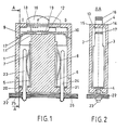
- Fig. 1 einen Längsschnitt durch eine schaltbare Kurzschlusssteck-Vorrichtung im zusammengesteckten Zustand,
- ; Fig. 2 einen Längsschnitt durch die Kurzschlusssteck-Vorrichtung nach Fig. 1 längs deren Linie AA.
- In einem Gehäuse 1 aus flammhemmendem Polyester, das aus zwei symmetrischen Hälften 2, 3 mit der Trennstelle 4. besteht, sind zwei federnde Kontakte 5, 6 aus Messung oder Berylliumkupfer mit Kontaktfedern 7, 8 verschiebungesicher angeordnet. Am einen Ende laufen die Kontakte in Kontaktzungen 9, 10 aus, die aufeinanderzu gebogen sind und am Ende je eine buckelförmige Auswölbung 11, 12 versehen sind. In der oberen Stirnfläche 13 des Gehäuses 1 ist ein in Nuten 14, 15 geführter Schieber 16 parallel zur oberen Stirnfläche 13 verschieblich angeordnet. Auf der dem Gehäuseinnern zugewandten Fläche des Schiebers 16 ist eine Kontaktplatte 17 eingelegt, deren Länge so bemessen ist, dass in der einen Endstellung 1 des Schiebers beide Kontaktzungen 9, 10 elektrisch miteinander verbunden sind, während in der anderen Endstellung 0 die genannten Teile elektrisch voneinander getrennt sind. Damit der Schieber in beiden Endstellungen 0, 1 einrastet, ist die dem Gehäuseinnern zugewandte Fläche der Kontaktplatte mit entsprechenden Vertiefungen 18, 19 versehen.
- Die untere Stirnfläche des Gehäuses weist zwei Bohrungen 20, 21 auf, die sich nach aussen kegelförmig erweitern. Die Kontakte 5, 6 samt den Kontaktfedern 7, 8 bilden somit in Verbindung mit dem beschriebenen Gehäuse paarig angeordnete Buchsen.
- In den Bauelementeträger, z.B. eine Leiterplatte 22 sind zwei Stifte 23, 24 im Abstand der beiden Bohrungen 20, 21 vorzugsweise im üblichen Rastermass, z.B, einem ganzzahligen Vielfachen von 1/10 Zoll eingelötet, welche an den beiden Kontaktfedern 7, 8 federnd anliegen, wodurch (im zusammengesteckten Zustand) die elektrische Verbindung zwischen den Kontaktzungen 9, 10 und Leiterbahnen 25, 26 auf der Lötseite der Leiterplatte 22 hergestellt ist.
- Analog zu den DIP-Schaltern können beliebige Programmier-Stecker aneinandergereiht werden, wobei benachbarte Kontaktpaare einen im Rastermass 1/10" liegenden Abstand aufweisen. Die maschinell in die Leiterplatte 22 gesetzten und verlöteten Stifte 23, 24 werden nach der kompletten Bestückung für die automatische Prüfung gruppenweise adaptiert und nach abgeschlossener Prüfung mit den Programmier-Steckern bestückt. Je nach schematischer Darstellung und Bestückungsdruck auf dem Bauelemententräger wird der Schieber 16 in die vorgeschriebene Stellung 0 oder I gebracht. Der Stecker kann nachträglich in der Anlagenprüfung oder vom Kunden selbst ohne Demontage des Gerätes bei Bedarf um- oder zugeschaltet werden.
Claims (3)
Applications Claiming Priority (2)
| Application Number | Priority Date | Filing Date | Title |
|---|---|---|---|
| CH150884 | 1984-03-26 | ||
| CH1508/84 | 1984-03-26 |
Publications (3)
| Publication Number | Publication Date |
|---|---|
| EP0158122A2 true EP0158122A2 (de) | 1985-10-16 |
| EP0158122A3 EP0158122A3 (en) | 1985-12-27 |
| EP0158122B1 EP0158122B1 (de) | 1989-01-04 |
Family
ID=4212076
Family Applications (1)
| Application Number | Title | Priority Date | Filing Date |
|---|---|---|---|
| EP85102598A Expired EP0158122B1 (de) | 1984-03-26 | 1985-03-07 | Programmier-Stecker |
Country Status (2)
| Country | Link |
|---|---|
| EP (1) | EP0158122B1 (de) |
| DE (1) | DE3567326D1 (de) |
Cited By (3)
| Publication number | Priority date | Publication date | Assignee | Title |
|---|---|---|---|---|
| FR2696048A1 (fr) * | 1992-09-23 | 1994-03-25 | Professional Gl Electro Produc | Dispositif de connexion pour installation de transmission de signaux. |
| WO2005050792A2 (en) * | 2003-11-18 | 2005-06-02 | Tyco Electronics Amp Gmbh | Connector socket |
| US20170290197A1 (en) * | 2014-08-29 | 2017-10-05 | Huawei Technologies Co., Ltd. | Electronic product |
Families Citing this family (1)
| Publication number | Priority date | Publication date | Assignee | Title |
|---|---|---|---|---|
| DE9215701U1 (de) * | 1992-11-19 | 1993-01-07 | Wissing, Heimo, Dr.Med. Dipl.-Ing., 6900 Heidelberg, De |
Citations (5)
| Publication number | Priority date | Publication date | Assignee | Title |
|---|---|---|---|---|
| FR1571487A (de) * | 1968-05-03 | 1969-06-20 | ||
| FR2223937A1 (de) * | 1973-03-29 | 1974-10-25 | Telemecanique Electrique | |
| US4116524A (en) * | 1977-06-29 | 1978-09-26 | Illinois Tool Works | Terminal bridging assembly |
| EP0018133A1 (de) * | 1979-04-23 | 1980-10-29 | AMP INCORPORATED (a New Jersey corporation) | Elektrischer Schalter mit mehreren Wählern |
| US4283100A (en) * | 1979-12-27 | 1981-08-11 | Western Electric Company, Inc. | Jumper plug |
-
1985
- 1985-03-07 EP EP85102598A patent/EP0158122B1/de not_active Expired
- 1985-03-07 DE DE8585102598T patent/DE3567326D1/de not_active Expired
Patent Citations (5)
| Publication number | Priority date | Publication date | Assignee | Title |
|---|---|---|---|---|
| FR1571487A (de) * | 1968-05-03 | 1969-06-20 | ||
| FR2223937A1 (de) * | 1973-03-29 | 1974-10-25 | Telemecanique Electrique | |
| US4116524A (en) * | 1977-06-29 | 1978-09-26 | Illinois Tool Works | Terminal bridging assembly |
| EP0018133A1 (de) * | 1979-04-23 | 1980-10-29 | AMP INCORPORATED (a New Jersey corporation) | Elektrischer Schalter mit mehreren Wählern |
| US4283100A (en) * | 1979-12-27 | 1981-08-11 | Western Electric Company, Inc. | Jumper plug |
Cited By (7)
| Publication number | Priority date | Publication date | Assignee | Title |
|---|---|---|---|---|
| FR2696048A1 (fr) * | 1992-09-23 | 1994-03-25 | Professional Gl Electro Produc | Dispositif de connexion pour installation de transmission de signaux. |
| EP0589786A1 (de) * | 1992-09-23 | 1994-03-30 | Professional General Electronic Products P.G.E.P. | Verbindervorrichtung für Signalübertragungseinrichtung |
| WO2005050792A2 (en) * | 2003-11-18 | 2005-06-02 | Tyco Electronics Amp Gmbh | Connector socket |
| WO2005050792A3 (en) * | 2003-11-18 | 2008-01-03 | Tyco Electronics Amp Gmbh | Connector socket |
| AU2004311206B2 (en) * | 2003-11-18 | 2008-11-13 | Tyco Electronics Amp Gmbh | Connector socket |
| US20170290197A1 (en) * | 2014-08-29 | 2017-10-05 | Huawei Technologies Co., Ltd. | Electronic product |
| US10130005B2 (en) * | 2014-08-29 | 2018-11-13 | Huawei Technologies Co., Ltd. | Electronic product |
Also Published As
| Publication number | Publication date |
|---|---|
| EP0158122B1 (de) | 1989-01-04 |
| EP0158122A3 (en) | 1985-12-27 |
| DE3567326D1 (en) | 1989-02-09 |
Similar Documents
| Publication | Publication Date | Title |
|---|---|---|
| DE4438802C1 (de) | Verteilerleisten mit Querverteilung der elektrischen Leistung (II) | |
| DE3603750A1 (de) | Automatisierungsgeraet | |
| DE3525085C2 (de) | ||
| DE3320418A1 (de) | Auf einer gemeinsamen tragschiene montierter apparatesatz | |
| DE2646616C3 (de) | Anreihbares Einbauteil | |
| DE3625580A1 (de) | Ventilanordnung | |
| DE2718442A1 (de) | Baugruppe mit einer eine gedruckte schaltung aufweisenden grundplatte und einer haltevorrichtung zur halterung und justierung elektronischer bauelemente | |
| EP0158122B1 (de) | Programmier-Stecker | |
| EP0308635A2 (de) | Anschlussvorrichtung der Fernmeldetechnik | |
| DE2722736C2 (de) | Mehrpolige Anschlußleiste | |
| DE6607308U (de) | Schalterzusammenbau mit einer kontaktverbindung zu einer gedruckten schaltung | |
| DE1257235B (de) | Baueinheit mit in mehreren Ebenen angeordneten gedruckten Leiterplatten | |
| DE2051052A1 (de) | Prüfvorrichtung zum Prüfen von geätzten Schaltungsplatten | |
| DE1276767B (de) | Pruefstellenkontakt zur Herstellung eines Pruefpunktes in einer elektrischen Schaltung auf einer gedruckten Schaltkarte | |
| DE2643186C2 (de) | Verteilerelement für Fernmeldevermittlungsanlagen | |
| DE2622054A1 (de) | Elektromagnetisches schaltgeraet | |
| DE1615576B1 (de) | Drahthaltevorrichtung | |
| DE2362143C3 (de) | ||
| DE1259427B (de) | Isolierstofftraegerplatte fuer ein elektrisches Nachrichtengeraet | |
| DE3133199C2 (de) | Kontaktsokel für elektrische Bauteile | |
| DE2050069C (de) | Kontakteinrichtung | |
| DE1124558B (de) | Gestellrahmenaufbau fuer Fernmelde-, insbesondere Fernsprechanlagen | |
| DE1615576C (de) | Drahthaltevornthtung | |
| DE2345327A1 (de) | Pruefeinrichtung fuer ein elektrisches geraet | |
| DE3414323A1 (de) | Elektrischer steckverbinder |
Legal Events
| Date | Code | Title | Description |
|---|---|---|---|
| PUAI | Public reference made under article 153(3) epc to a published international application that has entered the european phase |
Free format text: ORIGINAL CODE: 0009012 |
|
| AK | Designated contracting states |
Designated state(s): CH DE FR GB LI SE |
|
| PUAL | Search report despatched |
Free format text: ORIGINAL CODE: 0009013 |
|
| AK | Designated contracting states |
Designated state(s): CH DE FR GB LI SE |
|
| 17P | Request for examination filed |
Effective date: 19860524 |
|
| RAP1 | Party data changed (applicant data changed or rights of an application transferred) |
Owner name: BBC BROWN BOVERI AG |
|
| 17Q | First examination report despatched |
Effective date: 19871216 |
|
| GRAA | (expected) grant |
Free format text: ORIGINAL CODE: 0009210 |
|
| AK | Designated contracting states |
Kind code of ref document: B1 Designated state(s): CH DE FR GB LI SE |
|
| REF | Corresponds to: |
Ref document number: 3567326 Country of ref document: DE Date of ref document: 19890209 |
|
| PGFP | Annual fee paid to national office [announced via postgrant information from national office to epo] |
Ref country code: FR Payment date: 19890222 Year of fee payment: 5 |
|
| PGFP | Annual fee paid to national office [announced via postgrant information from national office to epo] |
Ref country code: SE Payment date: 19890224 Year of fee payment: 5 |
|
| PGFP | Annual fee paid to national office [announced via postgrant information from national office to epo] |
Ref country code: GB Payment date: 19890228 Year of fee payment: 5 |
|
| PG25 | Lapsed in a contracting state [announced via postgrant information from national office to epo] |
Ref country code: LI Effective date: 19890331 Ref country code: CH Effective date: 19890331 |
|
| GBT | Gb: translation of ep patent filed (gb section 77(6)(a)/1977) | ||
| ET | Fr: translation filed | ||
| PLBE | No opposition filed within time limit |
Free format text: ORIGINAL CODE: 0009261 |
|
| STAA | Information on the status of an ep patent application or granted ep patent |
Free format text: STATUS: NO OPPOSITION FILED WITHIN TIME LIMIT |
|
| REG | Reference to a national code |
Ref country code: CH Ref legal event code: PL |
|
| PG25 | Lapsed in a contracting state [announced via postgrant information from national office to epo] |
Ref country code: DE Effective date: 19891201 |
|
| 26N | No opposition filed | ||
| PG25 | Lapsed in a contracting state [announced via postgrant information from national office to epo] |
Ref country code: GB Effective date: 19900307 |
|
| PG25 | Lapsed in a contracting state [announced via postgrant information from national office to epo] |
Ref country code: SE Effective date: 19900308 |
|
| GBPC | Gb: european patent ceased through non-payment of renewal fee | ||
| PG25 | Lapsed in a contracting state [announced via postgrant information from national office to epo] |
Ref country code: FR Effective date: 19901130 |
|
| REG | Reference to a national code |
Ref country code: FR Ref legal event code: ST |
|
| EUG | Se: european patent has lapsed |
Ref document number: 85102598.1 Effective date: 19910110 |