EP0156258A2 - Light guide member for radiation image read-out - Google Patents
Light guide member for radiation image read-out Download PDFInfo
- Publication number
- EP0156258A2 EP0156258A2 EP85102957A EP85102957A EP0156258A2 EP 0156258 A2 EP0156258 A2 EP 0156258A2 EP 85102957 A EP85102957 A EP 85102957A EP 85102957 A EP85102957 A EP 85102957A EP 0156258 A2 EP0156258 A2 EP 0156258A2
- Authority
- EP
- European Patent Office
- Prior art keywords
- light
- face
- guide member
- total reflection
- input face
- Prior art date
- Legal status (The legal status is an assumption and is not a legal conclusion. Google has not performed a legal analysis and makes no representation as to the accuracy of the status listed.)
- Granted
Links
- 230000005855 radiation Effects 0.000 title claims abstract description 15
- 230000003287 optical effect Effects 0.000 claims abstract description 79
- OAICVXFJPJFONN-UHFFFAOYSA-N Phosphorus Chemical compound [P] OAICVXFJPJFONN-UHFFFAOYSA-N 0.000 claims abstract description 27
- 230000004936 stimulating effect Effects 0.000 claims abstract description 18
- 239000000463 material Substances 0.000 description 2
- 230000003595 spectral effect Effects 0.000 description 2
- 238000001228 spectrum Methods 0.000 description 2
- 238000002834 transmittance Methods 0.000 description 2
- 230000003247 decreasing effect Effects 0.000 description 1
- 230000001747 exhibiting effect Effects 0.000 description 1
- 239000010979 ruby Substances 0.000 description 1
- 229910001750 ruby Inorganic materials 0.000 description 1
- 239000004065 semiconductor Substances 0.000 description 1
- 238000000926 separation method Methods 0.000 description 1
- 230000000638 stimulation Effects 0.000 description 1
Images

Classifications
-
- G—PHYSICS
- G01—MEASURING; TESTING
- G01T—MEASUREMENT OF NUCLEAR OR X-RADIATION
- G01T1/00—Measuring X-radiation, gamma radiation, corpuscular radiation, or cosmic radiation
- G01T1/16—Measuring radiation intensity
- G01T1/20—Measuring radiation intensity with scintillation detectors
- G01T1/2012—Measuring radiation intensity with scintillation detectors using stimulable phosphors, e.g. stimulable phosphor sheets
- G01T1/2014—Reading out of stimulable sheets, e.g. latent image
Definitions
- This invention relates to a light guide member for guiding light emitted by a stimulable phosphor sheet to a photodetector during the image read-out step in a radiation image recording and reproducing system wherein the stimulable phosphor sheet is exposed to a radiation passing through an object to have a radiation image stored therein, the stimulable phosphor sheet carrying the radiation image stored therein is scanned by stimulating rays which cause it to emit light in proportion to the radiation energy stored, the emitted light is photoelectrically detected and converted to an electric image signal, and a visible image is reproduced by use of the electric image signal.
- the radiation image recording and reproducing system as described above is disclosed, for example, in U.S. Patent Nos. 4,258,264 and 4,315,318, and Japanese Unexamined Patent Publication No. 56(1981)-11395.
- the radiation image recording and reproducing system was also described in "Nikkan Kogyo Shinbun” (Daily Industrial Newspaper), June 23, 1981 edition, page 16.
- the light guide member used for image read-out in the radiation image recording and reproducing system is disclosed, for example, in U.S. Patent No. 4,346,295.
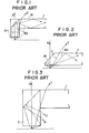
- Figures 1 and 2 are sectional side views showing embodiments of the light guide member described in Japanese Patent Application No. 58(1983)-218678, and Figure 3 is an enlarged view of Figure 1.
- stimulating rays entering the light guide member in the direction as indicated by the arrow A cause the stimulable phosphor sheet to emit light in the directions as indicated by the arrows Bl, B2 and C.
- the light emitted in the directions as indicated by the arrows Bl and B2 are reflected efficiently and guided inside of the light guide member.
- the light emitted in the direction as indicated by the arrow C comes out of the upper surface of a block 1.
- the light guide member as shown in Figure 1 is advantageous over the light guide member as shown in Figure 2 in that a photodetector such as a photomultiplier can be easily connected to the end portion of the block 1.
- the latter is advantageous over the former in that the height of the apparatus can be made small and the size of the whole apparatus can be decreased.
- the embodiment of Figure 1 is disadvantageous in that some components of the light emitted by the stimulable phosphor sheet come out of the light guide member as indicated by the arrows D and E. Thus it is desired to further improve the light guiding efficiency.
- the primary object of the present invention is to provide a light guide member exhibiting an improved light guiding efficiency by preventing the light emitted by a stimulable phosphor sheet from escaping from the light guide member.
- Another object of the present invention is to provide a light guide member which has a light output end spaced apart from the stimulable phosphor sheet and which is easily connected to a photodetector.
- the light guide member for radiation image read-out in accordance with the present invention comprises a first optical block having a light input face standing face to face with a stimulable phosphor sheet, a second optical block having a dichroic optical plane, and a third optical block having a light output face.
- the optical blocks are positioned adjacent to each other via small spaces for generating total reflection planes therebetween, so that light components C, D and E coming out of the light guide member as shown in Figure 3 are entirely reflected by the total reflection planes and are guided inside of the light guide member.
- boundary spaces air gaps for total reflection
- boundary spaces are formed horizontally from the lower end of the dichroic optical plane in the example of Figure 3 and vertically downwardly from the upper end thereof, and the light coming out of the light guide member is reflected at the boundary spaces inwardly of the light guide member.
- the horizontal and vertical total reflection planes are positioned adjacent the dichroic optical plane by forming the air gaps, the light emitted by the stimulable phosphor sheet and reflected by the dichroic optical plane is entirely reflected by the total reflection planes and is prevented from coming out of the light guide member. Therefore, it is possible to obtain a high light guiding .efficiency.
- the light guide member in accordance with the present invention comprises a first optical block 21, a second optical block 22, and a third optical block 23.
- the first optical block 21 is provided with a light input face 21A positioned close to and approximately in parallel with a stimulable phosphor sheet 10 carrying a radiation image stored therein to stand face to face therewith, a light output face 21B approximately parallel with the light input face 21A, a front total reflection plane 21C and a rear total reflection plane 21D extending vertically between the light input face 21A and the light output face 21B, and right and left total reflection planes extending vertically between the light input face 21A and the light output face 21B (only one of the right and left total reflection planes is designated by 21E in Figures 5 and 6).
- the second optical block 22 is provided with a light input face 22A standing face to face with the light output face 21B of the first optical block 21 via a small space 22a, a dichroic optical plane 22B extending upward obliquely from one end of the light input face 22A at an angle of approximately 45° with respect to the light input face 22A, the dichroic optical plane 22B transmitting the stimulating rays A and reflecting the light Sl to S4 emitted by the stimulable phosphor sheet 10, a light output face 22C extending vertically downward from an upper end of the dichroic optical plane 22B to the light input face 22A, and right and left total reflection planes extending vertically (only one of the right and left total reflection planes is designated by 22D in Figures 5 and 6).
- the third optical block 23 is provided with a light input face 23A standing face to face with the light output face 22C of the second optical block 22 via a small space 22b, an upper total reflection plane 23B extending approximately horizontally from the upper end of the light input face 23A, a lower total reflection plane 23C extending approximately horizontally from the lower end of the light input face 23A, two side faces forming right and left total reflection planes between the upper total reflection plane 23B and the lower total reflection plane 23C (only one of the side faces is designated by 23D in Figures 5 and 6), and a light output face 23E opposite to the light input face 23A.
- a triangular prism block 30 having a stimulating ray input face 31 normal to the stimulating rays A is closely contacted with the outer face of the dichroic optical plane 22B.
- the stimulating rays A entering from the stimulating ray input face 31 of the triangular prism block 30 pass through the dichroic optical plane 22B, the second optical block 22, the space 22a and the first optical block 21, and impinge upon the stimulable phosphor sheet 10.
- the stimulable phosphor sheet 10 When exposed to the stimulating rays A, the stimulable phosphor sheet 10 emits light as indicated by Sl to S4.
- the light component emitted by the stimulable phosphor sheet 10, entering from the light input face 21A and reflected by the front plane 21C of the first optical block 21 passes through the space 22a, and is then reflected by the dichroic optical plane 22B as indicated by Sl.
- the light component Sl then passes through the space 22b, enters the third optical block 23, and is guided inside of the third optical block 23 by total reflection.
- the light component S2 entering from the light input face 21A and passing through the space 22a to the dichroic optical plane 22B without being reflected by the front plane 21C of the first optical block 21 is entirely reflected by the light input face 22A of the second optical block 22 after being reflected by the dichroic optical plane 22B. Then the light component S2 passes through the space 22B, enters the third optical block 23, and is guided inside of the third optical block 23 by total reflection.
- the light component S3 entering from the light input face 21A and passing through the space 22a to the light output face 22C of the second optical block 22 without being reflected by the rear plane 21D of the first optical block 21 is entirely reflected by the light output face 22C and then by the dichroic optical plane 22B.
- the light component S3 passes through the space 22b, enters the third optical block 23, and is guided inside of the third optical block 23 by total reflection.
- the light component S4 entering from the light input face 21A, totally reflected by the rear plane 21D of the first optical block 21, and passing through the space 22a to the dichroic optical plane 22B passes through the space 22b after being reflected by the dichroic optical plane 22B, enters the third optical block 23, and is guided inside of the third optical block 23 by total reflection.
- the light guide member is extended in the width direction of the stimulable phosphor sheet 10, and the light output face 23E of the third optical block 23 is optically connected to light guiding blocks 40A, 40B, 40C and 40D.
- the light output ends of the blocks 40A to 40D are closely contacted with photomultipliers 50A, 50B, 50C and 50D.
- a single light guiding block 40 is optically connected to the light output face 23E of the third optical block 23 of Figure 5, and a photomultiplier 50 is closely contacted with the light output end of the light guiding block 40.
- the light guiding blocks 40A to 40D in Figure 5 and the light guiding block 40 in Figure 6 are prism blocks having the upper, lower, right and left faces constituted by total reflection planes, or prism blocks having the upper and lower faces constituted by total reflection planes, and the right and left faces provided with reflection films.
- the wavelength distribution of the stimulating rays should be different from and far apart from the wavelength distribution of the light emitted by the stimulable phosphor sheet 10.
- the spectrum of the stimulating rays should not overlap the spectrum of the light emitted by the stimulable phosphor sheet 10.
- the stimulating rays should preferably be a He-Ne laser beam (633nm), a YAG laser beam (1064nm), a ruby laser beam (694nm), a semiconductor laser beam (infrared rays), or the like, which has a wavelength longer than that of the light emitted by the stimulable phosphor sheet 10.
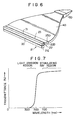
- the dichroic optical plane 22B should exhibit the spectral transmittance as shown in Figure 7 (when the angle of incidence is 45°). That is, it should transmit the stimulating rays A having a long wavelength, and reflects the light having a short wavelength (e.g. 300nm to 500nm) emitted by the stimulable phosphor sheet 10.
- a dichroic optical plane is fabricated, for example, of a plurality of layers of films of a high refractive index material and a low refractive index material.
Abstract
Description
- This invention relates to a light guide member for guiding light emitted by a stimulable phosphor sheet to a photodetector during the image read-out step in a radiation image recording and reproducing system wherein the stimulable phosphor sheet is exposed to a radiation passing through an object to have a radiation image stored therein, the stimulable phosphor sheet carrying the radiation image stored therein is scanned by stimulating rays which cause it to emit light in proportion to the radiation energy stored, the emitted light is photoelectrically detected and converted to an electric image signal, and a visible image is reproduced by use of the electric image signal.
- The radiation image recording and reproducing system as described above is disclosed, for example, in U.S. Patent Nos. 4,258,264 and 4,315,318, and Japanese Unexamined Patent Publication No. 56(1981)-11395. The radiation image recording and reproducing system was also described in "Nikkan Kogyo Shinbun" (Daily Industrial Newspaper), June 23, 1981 edition, page 16. The light guide member used for image read-out in the radiation image recording and reproducing system is disclosed, for example, in U.S. Patent No. 4,346,295.
- In order to improve the light guiding efficiency of the light guide member and to realize efficient image read-out with a small apparatus, the applicant proposed a novel light guide member provided with a dichroic optical plane in Japanese Patent Application No. 58(1983)-218678. However, a need exists for a light guide member further improved in design. Figures 1 and 2 are sectional side views showing embodiments of the light guide member described in Japanese Patent Application No. 58(1983)-218678, and Figure 3 is an enlarged view of Figure 1. In the embodiments of Figures 1 and 2, stimulating rays entering the light guide member in the direction as indicated by the arrow A cause the stimulable phosphor sheet to emit light in the directions as indicated by the arrows Bl, B2 and C. The light emitted in the directions as indicated by the arrows Bl and B2 are reflected efficiently and guided inside of the light guide member. However, the light emitted in the direction as indicated by the arrow C comes out of the upper surface of a block 1. The light guide member as shown in Figure 1 is advantageous over the light guide member as shown in Figure 2 in that a photodetector such as a photomultiplier can be easily connected to the end portion of the block 1. On the other hand, the latter is advantageous over the former in that the height of the apparatus can be made small and the size of the whole apparatus can be decreased.
- Further, as shown in Figure 3, the embodiment of Figure 1 is disadvantageous in that some components of the light emitted by the stimulable phosphor sheet come out of the light guide member as indicated by the arrows D and E. Thus it is desired to further improve the light guiding efficiency.
- . The primary object of the present invention is to provide a light guide member exhibiting an improved light guiding efficiency by preventing the light emitted by a stimulable phosphor sheet from escaping from the light guide member.
- Another object of the present invention is to provide a light guide member which has a light output end spaced apart from the stimulable phosphor sheet and which is easily connected to a photodetector.
- The light guide member for radiation image read-out in accordance with the present invention comprises a first optical block having a light input face standing face to face with a stimulable phosphor sheet, a second optical block having a dichroic optical plane, and a third optical block having a light output face. The optical blocks are positioned adjacent to each other via small spaces for generating total reflection planes therebetween, so that light components C, D and E coming out of the light guide member as shown in Figure 3 are entirely reflected by the total reflection planes and are guided inside of the light guide member. That is, in the present invention, boundary spaces (air gaps for total reflection) are formed horizontally from the lower end of the dichroic optical plane in the example of Figure 3 and vertically downwardly from the upper end thereof, and the light coming out of the light guide member is reflected at the boundary spaces inwardly of the light guide member.
- In the light guide member of the present invention, since the horizontal and vertical total reflection planes are positioned adjacent the dichroic optical plane by forming the air gaps, the light emitted by the stimulable phosphor sheet and reflected by the dichroic optical plane is entirely reflected by the total reflection planes and is prevented from coming out of the light guide member. Therefore, it is possible to obtain a high light guiding .efficiency.
-
- Figures 1 and 2 are side sectional views showing examples of the conventional light guide member used for radiation image read-out,
- Figure 3 is an enlarged view of Figure 1,
- Figure 4 is a side sectional view showing an embodiment of the light guide member in accordance with the present invention,
- Figures 5 and 6 are perspective views showing the light guide member of Figure 4 used together with a photodetector, and
- Figure 7 is a graph showing the spectral transmittance of the dichroic optical plane used in the present invention.
- The present invention will hereinbelow be described in further detail with reference to the accompanying drawings.
- Referring to Figure 4, the light guide member in accordance with the present invention comprises a first
optical block 21, a secondoptical block 22, and a thirdoptical block 23. The firstoptical block 21 is provided with a light input face 21A positioned close to and approximately in parallel with astimulable phosphor sheet 10 carrying a radiation image stored therein to stand face to face therewith, alight output face 21B approximately parallel with the light input face 21A, a fronttotal reflection plane 21C and a rear total reflection plane 21D extending vertically between the light input face 21A and thelight output face 21B, and right and left total reflection planes extending vertically between the light input face 21A and thelight output face 21B (only one of the right and left total reflection planes is designated by 21E in Figures 5 and 6). The secondoptical block 22 is provided with alight input face 22A standing face to face with thelight output face 21B of the firstoptical block 21 via asmall space 22a, a dichroicoptical plane 22B extending upward obliquely from one end of thelight input face 22A at an angle of approximately 45° with respect to thelight input face 22A, the dichroicoptical plane 22B transmitting the stimulating rays A and reflecting the light Sl to S4 emitted by thestimulable phosphor sheet 10, alight output face 22C extending vertically downward from an upper end of the dichroicoptical plane 22B to thelight input face 22A, and right and left total reflection planes extending vertically (only one of the right and left total reflection planes is designated by 22D in Figures 5 and 6). The thirdoptical block 23 is provided with alight input face 23A standing face to face with thelight output face 22C of the secondoptical block 22 via asmall space 22b, an uppertotal reflection plane 23B extending approximately horizontally from the upper end of thelight input face 23A, a lowertotal reflection plane 23C extending approximately horizontally from the lower end of thelight input face 23A, two side faces forming right and left total reflection planes between the uppertotal reflection plane 23B and the lowertotal reflection plane 23C (only one of the side faces is designated by 23D in Figures 5 and 6), and alight output face 23E opposite to thelight input face 23A. Atriangular prism block 30 having a stimulatingray input face 31 normal to the stimulating rays A is closely contacted with the outer face of the dichroicoptical plane 22B. - The stimulating rays A entering from the stimulating
ray input face 31 of thetriangular prism block 30 pass through the dichroicoptical plane 22B, the secondoptical block 22, thespace 22a and the firstoptical block 21, and impinge upon thestimulable phosphor sheet 10. When exposed to the stimulating rays A, thestimulable phosphor sheet 10 emits light as indicated by Sl to S4. The light component emitted by thestimulable phosphor sheet 10, entering from the light input face 21A and reflected by thefront plane 21C of the firstoptical block 21 passes through thespace 22a, and is then reflected by the dichroicoptical plane 22B as indicated by Sl. The light component Sl then passes through thespace 22b, enters the thirdoptical block 23, and is guided inside of the thirdoptical block 23 by total reflection. The light component S2 entering from the light input face 21A and passing through thespace 22a to the dichroicoptical plane 22B without being reflected by thefront plane 21C of the firstoptical block 21 is entirely reflected by thelight input face 22A of the secondoptical block 22 after being reflected by the dichroicoptical plane 22B. Then the light component S2 passes through thespace 22B, enters the thirdoptical block 23, and is guided inside of the thirdoptical block 23 by total reflection. The light component S3 entering from the light input face 21A and passing through thespace 22a to thelight output face 22C of the secondoptical block 22 without being reflected by the rear plane 21D of the firstoptical block 21 is entirely reflected by thelight output face 22C and then by the dichroicoptical plane 22B. Then, the light component S3 passes through thespace 22b, enters the thirdoptical block 23, and is guided inside of the thirdoptical block 23 by total reflection. The light component S4 entering from the light input face 21A, totally reflected by the rear plane 21D of the firstoptical block 21, and passing through thespace 22a to the dichroicoptical plane 22B passes through thespace 22b after being reflected by the dichroicoptical plane 22B, enters the thirdoptical block 23, and is guided inside of the thirdoptical block 23 by total reflection. - As described above, the components Sl to S4 of the light emitted by the
stimulable phosphor sheet 10 impinge upon the dichroicoptical plane 22B, enter the thirdoptical block 23, and are guided inside of the thirdoptical block 23 by total reflection up to thelight output face 23E of the thirdoptical block 23. Therefore, the light guiding efficiency of the light guide member is markedly improved over that of the light guide members as shown in Figures 1 and 3. - In Figure 5, the light guide member is extended in the width direction of the
stimulable phosphor sheet 10, and thelight output face 23E of the thirdoptical block 23 is optically connected to light guidingblocks blocks 40A to 40D are closely contacted withphotomultipliers - In Figure 6, a single
light guiding block 40 is optically connected to thelight output face 23E of the thirdoptical block 23 of Figure 5, and aphotomultiplier 50 is closely contacted with the light output end of thelight guiding block 40. - The light guiding
blocks 40A to 40D in Figure 5 and thelight guiding block 40 in Figure 6 are prism blocks having the upper, lower, right and left faces constituted by total reflection planes, or prism blocks having the upper and lower faces constituted by total reflection planes, and the right and left faces provided with reflection films. - In order to facilitate separation from the light emitted by the
stimulable phosphor sheet 10 upon stimulation thereof, the wavelength distribution of the stimulating rays should be different from and far apart from the wavelength distribution of the light emitted by thestimulable phosphor sheet 10. Namely, the spectrum of the stimulating rays should not overlap the spectrum of the light emitted by thestimulable phosphor sheet 10. Accordingly, the stimulating rays should preferably be a He-Ne laser beam (633nm), a YAG laser beam (1064nm), a ruby laser beam (694nm), a semiconductor laser beam (infrared rays), or the like, which has a wavelength longer than that of the light emitted by thestimulable phosphor sheet 10. - Therefore, the dichroic
optical plane 22B should exhibit the spectral transmittance as shown in Figure 7 (when the angle of incidence is 45°). That is, it should transmit the stimulating rays A having a long wavelength, and reflects the light having a short wavelength (e.g. 300nm to 500nm) emitted by thestimulable phosphor sheet 10. Such a dichroic optical plane is fabricated, for example, of a plurality of layers of films of a high refractive index material and a low refractive index material. When thetriangular prism block 30 is closely contacted with the dichroicoptical plane 22B, theblock 30 is optically joined with the multi-layer optical plane.
Claims (8)
Applications Claiming Priority (2)
| Application Number | Priority Date | Filing Date | Title |
|---|---|---|---|
| JP59050025A JPS60194404A (en) | 1984-03-15 | 1984-03-15 | Condensing body for reading out radiation picture information |
| JP50025/84 | 1984-03-15 |
Publications (3)
| Publication Number | Publication Date |
|---|---|
| EP0156258A2 true EP0156258A2 (en) | 1985-10-02 |
| EP0156258A3 EP0156258A3 (en) | 1987-08-26 |
| EP0156258B1 EP0156258B1 (en) | 1989-08-23 |
Family
ID=12847456
Family Applications (1)
| Application Number | Title | Priority Date | Filing Date |
|---|---|---|---|
| EP85102957A Expired EP0156258B1 (en) | 1984-03-15 | 1985-03-14 | Light guide member for radiation image read-out |
Country Status (4)
| Country | Link |
|---|---|
| US (1) | US4591714A (en) |
| EP (1) | EP0156258B1 (en) |
| JP (1) | JPS60194404A (en) |
| DE (1) | DE3572542D1 (en) |
Cited By (1)
| Publication number | Priority date | Publication date | Assignee | Title |
|---|---|---|---|---|
| FR2595145A1 (en) * | 1986-02-28 | 1987-09-04 | Thomson Csf | MEMORY VISUALIZATION SYSTEM |
Families Citing this family (14)
| Publication number | Priority date | Publication date | Assignee | Title |
|---|---|---|---|---|
| JPS6190570A (en) * | 1984-10-11 | 1986-05-08 | Fuji Photo Film Co Ltd | Reader or radiation image information |
| CA1262190A (en) * | 1985-07-16 | 1989-10-03 | Terumi Matsuda | Image read-out apparatus |
| DE3543089A1 (en) * | 1985-12-05 | 1987-06-11 | Siemens Ag | DEVICE FOR CONVERTING RADIO IMAGE INFORMATION CARRIED IN A STORAGE LAYER INTO AN ELECTRICAL SIGNAL SEQUENCE |
| US4818861A (en) * | 1986-06-25 | 1989-04-04 | Hitachi Medical Corp. | Film image reading out device |
| US4742225A (en) * | 1986-10-16 | 1988-05-03 | Eastman Kodak Company | Elliptical cylinder light collector for photosimulable phosphor imaging apparatus |
| NL8902295A (en) * | 1989-09-14 | 1991-04-02 | Philips Nv | Apparatus for scanning a document along an optical path. |
| US5442533A (en) * | 1994-06-22 | 1995-08-15 | Eastman Kodak Company | High efficiency linear light source |
| US5506417A (en) * | 1994-11-21 | 1996-04-09 | Eastman Kodak Company | Light collector for photostimulable phosphor imaging systems |
| US5541421A (en) * | 1994-11-21 | 1996-07-30 | Eastman Kodak Company | Light collector having optically coated acrylic substrate |
| US6247645B1 (en) * | 1999-01-25 | 2001-06-19 | International Business Machines Corporation | Optical reader with combined housing and light pipe |
| US7075100B2 (en) | 2003-09-22 | 2006-07-11 | Honeywell International Inc. | Confocal scanner system and method |
| WO2008133765A2 (en) * | 2007-02-13 | 2008-11-06 | Sentinel Scanning Corporation | Ct scanning and contraband detection |
| EP2438429A4 (en) * | 2009-06-05 | 2014-04-30 | Sentinel Scanning Corp | Transportation container inspection system and method |
| JP5996478B2 (en) | 2013-04-09 | 2016-09-21 | 浜松ホトニクス株式会社 | Radiation image detector |
Citations (4)
| Publication number | Priority date | Publication date | Assignee | Title |
|---|---|---|---|---|
| DE539253C (en) * | 1927-06-04 | 1931-11-24 | Lorenz Akt Ges C | Device for image scanning for remote image transmission |
| DE2363995A1 (en) * | 1973-01-02 | 1974-07-04 | Eastman Kodak Co | METHOD FOR GENERATING A RADIOGRAPHIC IMAGE AND DEVICE FOR CARRYING OUT THE METHOD |
| US4346295A (en) * | 1978-12-26 | 1982-08-24 | Fuji Photo Film Co., Ltd. | Radiation image read out device |
| EP0064736A1 (en) * | 1981-05-09 | 1982-11-17 | DR.-ING. RUDOLF HELL GmbH | Light pick-up device |
Family Cites Families (5)
| Publication number | Priority date | Publication date | Assignee | Title |
|---|---|---|---|---|
| JPS5512429A (en) * | 1978-07-12 | 1980-01-29 | Fuji Photo Film Co Ltd | Radioactive image reader |
| US4485302A (en) * | 1978-12-26 | 1984-11-27 | Fuji Photo Film Co., Ltd. | Radiation image read out device |
| US4315318A (en) * | 1978-12-26 | 1982-02-09 | Fuji Photo Film Co., Ltd. | Method and apparatus for processing a radiation image |
| NL8103599A (en) * | 1981-07-30 | 1983-02-16 | Philips Nv | DEVICE FOR OPTICAL SCANNING OF A DOCUMENT. |
| US4454424A (en) * | 1981-09-29 | 1984-06-12 | The United States Of America As Represented By The United States Department Of Energy | Neutron position-sensitive scintillation detector |
-
1984
- 1984-03-15 JP JP59050025A patent/JPS60194404A/en active Granted
-
1985
- 1985-03-13 US US06/711,167 patent/US4591714A/en not_active Expired - Lifetime
- 1985-03-14 EP EP85102957A patent/EP0156258B1/en not_active Expired
- 1985-03-14 DE DE8585102957T patent/DE3572542D1/en not_active Expired
Patent Citations (4)
| Publication number | Priority date | Publication date | Assignee | Title |
|---|---|---|---|---|
| DE539253C (en) * | 1927-06-04 | 1931-11-24 | Lorenz Akt Ges C | Device for image scanning for remote image transmission |
| DE2363995A1 (en) * | 1973-01-02 | 1974-07-04 | Eastman Kodak Co | METHOD FOR GENERATING A RADIOGRAPHIC IMAGE AND DEVICE FOR CARRYING OUT THE METHOD |
| US4346295A (en) * | 1978-12-26 | 1982-08-24 | Fuji Photo Film Co., Ltd. | Radiation image read out device |
| EP0064736A1 (en) * | 1981-05-09 | 1982-11-17 | DR.-ING. RUDOLF HELL GmbH | Light pick-up device |
Cited By (3)
| Publication number | Priority date | Publication date | Assignee | Title |
|---|---|---|---|---|
| FR2595145A1 (en) * | 1986-02-28 | 1987-09-04 | Thomson Csf | MEMORY VISUALIZATION SYSTEM |
| EP0240384A1 (en) * | 1986-02-28 | 1987-10-07 | Thomson-Csf | Memory imaging system |
| US4818877A (en) * | 1986-02-28 | 1989-04-04 | Thomson-Csf | Memory display system |
Also Published As
| Publication number | Publication date |
|---|---|
| EP0156258B1 (en) | 1989-08-23 |
| JPH0426456B2 (en) | 1992-05-07 |
| JPS60194404A (en) | 1985-10-02 |
| DE3572542D1 (en) | 1989-09-28 |
| EP0156258A3 (en) | 1987-08-26 |
| US4591714A (en) | 1986-05-27 |
Similar Documents
| Publication | Publication Date | Title |
|---|---|---|
| US4591714A (en) | Light guide member for radiation image read-out | |
| US4629890A (en) | Radiation image read-out apparatus | |
| KR940004777B1 (en) | Reading device for stimulable phosphor panel | |
| KR101855599B1 (en) | Cr reader a light collector using optic fibers and a subsidiary mirror | |
| US5483081A (en) | Method for detecting light emitted by two surfaces of a stimulable phosphor sheet | |
| EP0330662B1 (en) | Light collector for photo-stimulable phosphor imaging apparatus | |
| EP0209186B1 (en) | Image recording and readout device based on light-stimulable phosphors | |
| EP0156259B1 (en) | Light guide member for radiation image read-out | |
| US4818880A (en) | Radiation image read-out apparatus | |
| JPS6051099B2 (en) | Radiation image information reading device | |
| EP0144856B1 (en) | Radiation image read-out apparatus | |
| US4970394A (en) | Apparatus for reading-out stimulable phosphor, radiographic recording elements | |
| KR101829554B1 (en) | Cr reader comprising a light collector using a bundle of optical fiber | |
| JP2557261B2 (en) | Reader | |
| EP0493126A2 (en) | A radiation data image reader | |
| US4950904A (en) | Radiation image read-out apparatus | |
| JP2952453B2 (en) | Double-sided condensing phosphor sheet reading method | |
| JPH0556491B2 (en) | ||
| JPS63236464A (en) | Radiation picture information reader | |
| JPH0813080B2 (en) | Radiation image information reader | |
| JPS61290857A (en) | Reader for radiation picture image information | |
| JPS61162036A (en) | Radiation picture information reader | |
| JPS60189736A (en) | Reader for radiation image information | |
| JPH0795189B2 (en) | Image information recording and reading method | |
| JPS63236025A (en) | Light guide |
Legal Events
| Date | Code | Title | Description |
|---|---|---|---|
| PUAI | Public reference made under article 153(3) epc to a published international application that has entered the european phase |
Free format text: ORIGINAL CODE: 0009012 |
|
| AK | Designated contracting states |
Designated state(s): DE FR NL |
|
| PUAL | Search report despatched |
Free format text: ORIGINAL CODE: 0009013 |
|
| RHK1 | Main classification (correction) |
Ipc: G01T 1/29 |
|
| AK | Designated contracting states |
Kind code of ref document: A3 Designated state(s): DE FR NL |
|
| 17P | Request for examination filed |
Effective date: 19871007 |
|
| 17Q | First examination report despatched |
Effective date: 19881229 |
|
| GRAA | (expected) grant |
Free format text: ORIGINAL CODE: 0009210 |
|
| AK | Designated contracting states |
Kind code of ref document: B1 Designated state(s): DE FR NL |
|
| REF | Corresponds to: |
Ref document number: 3572542 Country of ref document: DE Date of ref document: 19890928 |
|
| ET | Fr: translation filed | ||
| PLBE | No opposition filed within time limit |
Free format text: ORIGINAL CODE: 0009261 |
|
| STAA | Information on the status of an ep patent application or granted ep patent |
Free format text: STATUS: NO OPPOSITION FILED WITHIN TIME LIMIT |
|
| 26N | No opposition filed | ||
| PGFP | Annual fee paid to national office [announced via postgrant information from national office to epo] |
Ref country code: NL Payment date: 20040216 Year of fee payment: 20 |
|
| PGFP | Annual fee paid to national office [announced via postgrant information from national office to epo] |
Ref country code: FR Payment date: 20040318 Year of fee payment: 20 |
|
| PGFP | Annual fee paid to national office [announced via postgrant information from national office to epo] |
Ref country code: DE Payment date: 20040430 Year of fee payment: 20 |
|
| PG25 | Lapsed in a contracting state [announced via postgrant information from national office to epo] |
Ref country code: NL Free format text: LAPSE BECAUSE OF EXPIRATION OF PROTECTION Effective date: 20050314 |
|
| NLV7 | Nl: ceased due to reaching the maximum lifetime of a patent |
Effective date: 20050314 |