EP0154765A2 - Apparatus for directly powering a multi-chip module from a power distribution bus - Google Patents
Apparatus for directly powering a multi-chip module from a power distribution bus Download PDFInfo
- Publication number
- EP0154765A2 EP0154765A2 EP85100003A EP85100003A EP0154765A2 EP 0154765 A2 EP0154765 A2 EP 0154765A2 EP 85100003 A EP85100003 A EP 85100003A EP 85100003 A EP85100003 A EP 85100003A EP 0154765 A2 EP0154765 A2 EP 0154765A2
- Authority
- EP
- European Patent Office
- Prior art keywords
- module
- voltage
- power
- tab
- integrated circuit
- Prior art date
- Legal status (The legal status is an assumption and is not a legal conclusion. Google has not performed a legal analysis and makes no representation as to the accuracy of the status listed.)
- Granted
Links
Images


Classifications
-
- H—ELECTRICITY
- H05—ELECTRIC TECHNIQUES NOT OTHERWISE PROVIDED FOR
- H05K—PRINTED CIRCUITS; CASINGS OR CONSTRUCTIONAL DETAILS OF ELECTRIC APPARATUS; MANUFACTURE OF ASSEMBLAGES OF ELECTRICAL COMPONENTS
- H05K1/00—Printed circuits
- H05K1/02—Details
- H05K1/0213—Electrical arrangements not otherwise provided for
- H05K1/0263—High current adaptations, e.g. printed high current conductors or using auxiliary non-printed means; Fine and coarse circuit patterns on one circuit board
-
- G—PHYSICS
- G06—COMPUTING; CALCULATING OR COUNTING
- G06F—ELECTRIC DIGITAL DATA PROCESSING
- G06F1/00—Details not covered by groups G06F3/00 - G06F13/00 and G06F21/00
- G06F1/16—Constructional details or arrangements
- G06F1/18—Packaging or power distribution
- G06F1/189—Power distribution
-
- H—ELECTRICITY
- H05—ELECTRIC TECHNIQUES NOT OTHERWISE PROVIDED FOR
- H05K—PRINTED CIRCUITS; CASINGS OR CONSTRUCTIONAL DETAILS OF ELECTRIC APPARATUS; MANUFACTURE OF ASSEMBLAGES OF ELECTRICAL COMPONENTS
- H05K2201/00—Indexing scheme relating to printed circuits covered by H05K1/00
- H05K2201/09—Shape and layout
- H05K2201/09145—Edge details
- H05K2201/0919—Exposing inner circuit layers or metal planes at the side edge of the PCB or at the walls of large holes
-
- H—ELECTRICITY
- H05—ELECTRIC TECHNIQUES NOT OTHERWISE PROVIDED FOR
- H05K—PRINTED CIRCUITS; CASINGS OR CONSTRUCTIONAL DETAILS OF ELECTRIC APPARATUS; MANUFACTURE OF ASSEMBLAGES OF ELECTRICAL COMPONENTS
- H05K2201/00—Indexing scheme relating to printed circuits covered by H05K1/00
- H05K2201/10—Details of components or other objects attached to or integrated in a printed circuit board
- H05K2201/10227—Other objects, e.g. metallic pieces
- H05K2201/10272—Busbars, i.e. thick metal bars mounted on the PCB as high-current conductors
-
- H—ELECTRICITY
- H05—ELECTRIC TECHNIQUES NOT OTHERWISE PROVIDED FOR
- H05K—PRINTED CIRCUITS; CASINGS OR CONSTRUCTIONAL DETAILS OF ELECTRIC APPARATUS; MANUFACTURE OF ASSEMBLAGES OF ELECTRICAL COMPONENTS
- H05K3/00—Apparatus or processes for manufacturing printed circuits
- H05K3/46—Manufacturing multilayer circuits
- H05K3/4611—Manufacturing multilayer circuits by laminating two or more circuit boards
- H05K3/4641—Manufacturing multilayer circuits by laminating two or more circuit boards having integrally laminated metal sheets or special power cores
Definitions
- the present invention pertains to printed circuit board packaging technology, and, more particularly, to a method and apparatus for powering a module, mounted on the printed circuit board, directly from a power distribution bus rather than powering the module from the power distribution bus by way of the printed circuit board.
- High performance is measured in terms of cycle time and the number of cycles per instruction.
- the number of circuits on an integrated circuit chip must increase.
- the number of integrated circuit chips must also increase.
- the introduction of high density integrated circuit packages, such as a Thermal Conduction Module, has provided for the increased number of integrated circuit chips necessary to produce the required high performance.
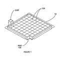
- a module such as module 10 shown in FIG. 1, has a plurality of integrated circuit chips 10a mounted thereon.
- the module 10 is mounted on a printed circuit board 12, the module being connected to various power distribution planes 12a within the board.
- the planes 12a are connected to a power distribution bus 14 thereby carrying the required current and providing the required voltage to the module 10 as necessary to power the chips 10a mounted on the module.
- the module 10 includes a multitude of input/output pins 10b connected to the power distribution planes 12a in the printed circuit board 12 for conducting the voltage and current to the chips lOa.
- the number of circuits on a chip has increased and the number of chips mounted on a module has increased in response to the demand for increased performance of large-scale computers
- the number of required pins on the module has also increased, these pins including signal pins to provide the necessary information signals to the chips and power distribution pins to provide the necessary voltage and current to power the chips.
- the number of required pins has increased, the number of power distribution planes in the printed circuit board also increased. Therefore, the thickness of the board has increased. As a result of the increased board thickness, greater power losses are experienced. Board manufacturing complexity also increases as board thickness increases.
- the module must be larger to accommodate the required number of pins.
- the trend, in the design of a computer system is toward miniaturization of computer system components, not toward enlarging the size of these components.
- the prior art packaging system could not meet the demand for an increased number of circuits and a resultant increase in the number of integrated circuit chips mounted on a module and, simultaneously, minimize its power losses as well as meet the demand for the miniaturization of computer system components.
- Antoher packaging system design is needed to simultaneously achieve the following desired objectives, that is, to increase the performance associated with a computer system, to minimize the power losses associated with the computer system components, and to maintain the trend toward the miniaturization of the computer system components.
- the substrate of the module includes a plurality of voltage distribution planes extending longitudinally and transversely through the substrate, the planes being connected to one or more voltage tabs mounted on the edge of the module substrate.
- the voltage tabs are connected directly to a power distribution bus.
- Input/output signal pins are disposed on the bottom surface of the module substrate for the conduction of a required signal to the module integrated circuit chips. Input/output power distribution pins are not needed on the bottom surface of the module substrate for powering the chips.
- One or more voltage distribution stripes can be disposed on the bottom surface of the module substrate, supplementing the voltage distribution planes internal to the module, for powering a remotely-located chip. Consequently, in spite of the increased number of circuits on a chip, and the increased number of chips needed for the required high performance of the computer system, fewer pins are needed on the bottom surface of the module substrate than was previously required. The power losses associated with the powering of the chips on the module are kept at a minimum and the small size of the module is maintained.
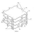
- FIG. 3 a perspective view of a module 10 is illustrated.
- a plurality of voltage distribution tabs 16 are connected to the edge of the module substrate for conducting a voltage and a current to the integrated circuit chips 10a disposed on the module 10. The voltage and the current are needed to power the chips.
- Each of the tabs 16 connects to a base plate 18 via an insulating material 17.
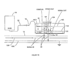
- FIG. 4 the direct module powering concept according to the present invention is illustrated.
- a printed circuit board 12 is illustrated.
- a module 10 is mounted on the board 12 and is connected thereto via a plurality of signal distribution input/output (1/0) pins 20.
- a voltage tab 16 is shown connected to the edge of the substrate of module 10. The voltage tab 16 is connected directly to a power distribution bus 14 via a power feed tab 22.
- the module 10 includes a plurality of voltage distribution planes 10c extending longitudinally and transversely through the module, each plane being substantially parallel to each other plane within the module.
- the voltage tabs 16 are connected to the edges of one or more of the voltage distribution planes 10c via a metallic interface 24 and a brazing compound 26 disposed between the metallic interface 24 and the voltage tab 16.
- the tab 16 comprises a copper-carbon composite or other suitable material with compatible physical and electrical properties.
- the module 10 also includes one or more voltage reference (or ground) planes 10d extending longitudinally and transversely through the module, each of the voltage reference planes being substantially parallel to each of the other planes within the module.
- a plurality of plated vias 10e extend orthogonally through the module 10, the vias being an electrical conducting material, such as copper.
- the electrical conducting material associated with each via 10e electrically connects the selected voltage distribution planes 10c to chips 10a and connects the selected voltage reference planes 10d to chips 10a thereby providing an electrical conducting path between the voltage distribution plane 10c, the chips 10a, and the voltage reference plane 10d.
- a plurality of voltage distribution stripes lOg are disposed on the bottom surface of the module 10 and are connected to selected plated vias 10e for providing an alternate path for the required voltage and current from voltage tab 16 necessary to power the chips 10a disposed on the module 10.
- tab 16 may be directly connected to stripes 10g in order to provide an additional conduction path.
- the current is conducted along a path consisting of a voltage tab 16, the brazing compound 26, the metallic interface 24, a voltage distribution plane 10c, a plated via 10e, a voltage stripe 10g, another plated via 10e, and the remotely-located chip 10a.
- a plurality of integrated circuit chips 10a are connected to the plated vias 10e via solder balls 10f for providing the electrical communication path between the chips 10a and the vias 10e.
- a voltage tab 16 is connected to the chip 10a via the brazing compound 26, the metallic interface 24, the voltage distribution plane 10c, the plated via 10e, and the solder ball.
- the chip 10a is connected to another voltage tab 16 via a solder ball 10f, a plated via 10e, the voltage reference (ground) plane 10d, a metallic interface 24, and the brazing compound 26.
- the printed circuit board 12 includes a plurality of voltage planes 12b. These planes 12b include voltage and current signal planes, such as plane 12bl, connected to a source of signal current and at least one ground plane, such as plane 12b2, connected to a ground potential. The signal planes are used to carry the signal current to the integrated circuit chips 10a via the pins 20 and the ground plane is used to carry the return signal current from the chips to ground via pins 20.
- the board 12 includes a plurality of plated vias 12c. When the module 10 is mounted on the board 12, the pins 20 are disposed within the plated vias 12c. The vias 12c provide an electrical communication path between the pins 20 and the voltage planes 12b.
- each of the planes 10c and 10d include a plurality of extended tabs 10cl disposed on each of the four sides thereof for communicating electrically with a voltage tab 16.
- Each extended tab 10cl is in contact with a metallic interface 24 of FIG. 4.
- the metallic interface 24 is connected to a voltage tab 16 via the brazing compound 26.
- the voltage tab 16 is exposed to a particular voltage potential for energizing the integrated circuit chips disposed on the module 10.
- the metallic interface 24 may be diposed in contact with two of the extended tabs 10cl. In this way, the voltage planes 10c, having the extended tabs 10cl in contact with the metallic interface 24, will each be exposed to the same voltage potential as carried by the voltage tab 16 connected thereto.
- FIGS. 5b and 5c a bottom view of the voltage distribution metallization layer 10c and the voltage reference metallization layer 10d, taken along section lines A-A and B-B shown in FIG. 4, is illustrated.
- a bottom view of the voltage reference layer 10d is shown, the layer including a through hole 10dl and a through hole lOd2.
- Through hole 10dl has a diameter dl whereas through hole 10d2 has a diameter d2.
- diameter dl is greater than diameter d2.
- Diameter d2 is smaller since electrical contact must be made with a metallic plating in its via 10e in order to provide a return path for current from chip 10a. The current returns to ground potential via extended tab 10cl.
- FIG. 5c a bottom view of the voltage distribution layer 10c is shown, the layer including a through hole 10cl and a through hole 10c2.
- Through hole 10cl has a diameter d3 whereas through hole lOc2 has a diameter d4.
- diameter d4 is greater than diameter d3.
- Diameter d3 is smaller since electrical contact must be made with a metallic plating in its via 10e in order to provide a path for current from the power distribution bus 14 to chip 10a. Since diameters dl and d4 are larger than diameters d2 and d3, respectively, no such electrical contact is made between the metallization layers associated with through holes lOdl and 10c2 and the metallic plating in their vias 10e.
- FIG. 6 a perspective view of the bottom surface of module 10 is illustrated.
- the bottom surface of module 10 includes a multitude of input/output signal pins 20. These pins carry the necessary signal current to the chips lOa, and are not used to power the chips 10a.
- the pins 20 are arranged in groups.
- a voltage distribution stripe 10g is disposed between adjacent groups of the pins 20 for the purpose of powering remotely-located chips 10a relative to the voltage tab 16 exposed to the voltage from the power source 14.
- the current necessary to power a remotely-located chip lOa traverses a path consisting of the voltage tab 16, brazing compound 26, metallic interface 24, the extended tab 10cl of a voltage distribution plane 10c, a plated via 10e, a voltage distribution stripe 10g, another plated via 10e, and the solder ball 10f of the remotely-located chip 10a.
- module 10 is powered directly from bus 14 via voltage tab 16.
- the required voltage and current, needed to power the chips 10a on the module 10 traverses a path indicated in the drawing by voltage tab 16, voltage distribution layer 10c and plated via 10e.
- This path is annotated in the drawing by the label "power-in”.
- the return path for the required current, to ground potential is annotated in the drawing by the label "power-out”, the return current traversing a path indicated by plated via 10e, and voltage reference layer 10d.
- the reference layer is connected to another tab 16 connected to ground potential.
- the voltage reference layer 10d is maintained at ground potential by virtue of its connection to ground plane 12b2 in the printed circuit board 12.
- the required signal current is provided via signal plane 12bl, the signal current provided to module 10 via a path indicated by signal plane 12bl, pin 20, plated via 10e, and solder ball 10f.
- the required signal current is annotated in the drawing by the label "signal-in”.
- the signal current returns to ground potential by way of solder ball 10f, plated via 10e and voltage reference layer 10d.
- the return signal current is annotated in the drawing by the label "signal-out”.
- FIG. 7b illustrates this functional operation, of this one embodiment of the present invention, in three dimensions.
- module 10 is powered directly from bus 14 via voltage tab 16.
- the current required to power the chips 10a on module 10 traverses a path indicated by tab 16, extended tab 10cl of voltage distribution layer 10c, plated via 10e, voltage distribution stripe 10g, another plated via 10e, and solder ball 10f.
- This required current is annotated in the drawing by the label "power-in”.
- the current returns to ground potential by way of plated via 10e, voltage reference layer 10d, another extended tab 10cl, and another voltage tab 16.
- the return current is annotated in the drawing by the label "power-out”.
- the voltage reference layer 10d is maintained at ground potential by virtue of ground plane 12b2 in the printed circuit board 12.
- the signal current required by the chip 10a on the module 10 is provided by signal plane 12b1 in board 12, the signal current traversing a path to module 10 indicated by signal plane 12bl and plated via 10e.
- the required signal current is annotated in the drawing by the label "signal-in”.
- the return path for the signal current is provided by plated via 10e, voltage reference layer 10d, another extended tab 10cl of voltage reference layer 10d, and another voltage tab 16.
- the return signal current is annotated in the drawing by the label "signal-out”.
- FIG. 7d illustrates this functional operation, of another embodiment of the present invention, in three dimensions.
Abstract
Description
- The present invention pertains to printed circuit board packaging technology, and, more particularly, to a method and apparatus for powering a module, mounted on the printed circuit board, directly from a power distribution bus rather than powering the module from the power distribution bus by way of the printed circuit board.
- The computers of the future will require a high throughput performance. High performance is measured in terms of cycle time and the number of cycles per instruction. However, in order to achieve this high performance, the number of circuits on an integrated circuit chip must increase. Further, the number of integrated circuit chips must also increase. The introduction of high density integrated circuit packages, such as a Thermal Conduction Module, has provided for the increased number of integrated circuit chips necessary to produce the required high performance.
- However, with the introduction of these high density integrated circuit packages, two undesirable side effects are noticeable: (1) the power dissipated by a package is higher than previously experienced, and (2) the required current supplied to the package has increased significantly. These high circuit density integrated circuit packages necessitate the use of a large number of input/output (non-signal) pins to power the chips and to maintain power losses and voltage drops at reasonable levels. This requirement for more pins is compounded by the simultaneous demand for an increased number of input/output signal pins required to conduct the necessary signals to or from the increased number of circuits on the chips.
- Furthermore, the demand for an increased number of circuits renders difficult the design of a modular or granular system. If a system is highly modular or granular in nature, it is easy to maintain and service by field representatives.
- In prior art printed circuit board packaging system designs, a module, such as
module 10 shown in FIG. 1, has a plurality of integrated circuit chips 10a mounted thereon. Referring to FIG. 2, themodule 10 is mounted on a printedcircuit board 12, the module being connected to various power distribution planes 12a within the board. The planes 12a are connected to apower distribution bus 14 thereby carrying the required current and providing the required voltage to themodule 10 as necessary to power the chips 10a mounted on the module. Themodule 10 includes a multitude of input/output pins 10b connected to the power distribution planes 12a in the printedcircuit board 12 for conducting the voltage and current to the chips lOa. Since the number of circuits on a chip has increased and the number of chips mounted on a module has increased in response to the demand for increased performance of large-scale computers, the number of required pins on the module has also increased, these pins including signal pins to provide the necessary information signals to the chips and power distribution pins to provide the necessary voltage and current to power the chips. Since the number of required pins has increased, the number of power distribution planes in the printed circuit board also increased. Therefore, the thickness of the board has increased. As a result of the increased board thickness, greater power losses are experienced. Board manufacturing complexity also increases as board thickness increases. - Furthermore, due to the increased number of pins, the module must be larger to accommodate the required number of pins. However, the trend, in the design of a computer system, is toward miniaturization of computer system components, not toward enlarging the size of these components.
- Therefore, the prior art packaging system could not meet the demand for an increased number of circuits and a resultant increase in the number of integrated circuit chips mounted on a module and, simultaneously, minimize its power losses as well as meet the demand for the miniaturization of computer system components. Antoher packaging system design is needed to simultaneously achieve the following desired objectives, that is, to increase the performance associated with a computer system, to minimize the power losses associated with the computer system components, and to maintain the trend toward the miniaturization of the computer system components.
- Accordingly, it is a primary object of the present invention to provide another printed circuit board packaging system design capable of achieving the above mentioned desired objectives.
- It is another object of the present invention to provide another printed circuit board packaging system design involving a direct module powering approach for powering the integrated circuit chips on a module whereby the module is powered directly from the power distribution bus rather than from the bus via the power distribution planes within the board and the input/output pins mounted on the bottom of the module substrate.
- These and other objects of the present invention, as claimed, are fulfilled by utilizing a direct module powering approach for powering the integrated circuit chips mounted on a module connected to a printed circuit board. The substrate of the module includes a plurality of voltage distribution planes extending longitudinally and transversely through the substrate, the planes being connected to one or more voltage tabs mounted on the edge of the module substrate. The voltage tabs are connected directly to a power distribution bus. Input/output signal pins are disposed on the bottom surface of the module substrate for the conduction of a required signal to the module integrated circuit chips. Input/output power distribution pins are not needed on the bottom surface of the module substrate for powering the chips. One or more voltage distribution stripes can be disposed on the bottom surface of the module substrate, supplementing the voltage distribution planes internal to the module, for powering a remotely-located chip. Consequently, in spite of the increased number of circuits on a chip, and the increased number of chips needed for the required high performance of the computer system, fewer pins are needed on the bottom surface of the module substrate than was previously required. The power losses associated with the powering of the chips on the module are kept at a minimum and the small size of the module is maintained.
- In addition, since there is an increasing need for more signal pins on modules to conduct desired voltage signals to the module chips, and since power distribution pins are no longer needed by the modules, more signal pins may be disposed on the bottom surface of the module for the conduction of required voltage signals to or from the module chips.
- Further scope of applicability of the present invention will become apparent from the detailed description presented hereinafter. It should be understood, however, that the detailed description and the specific examples, while representing a preferred embodiment of the invention, are given by way of illustration only, since various changes and modifications within the scope of the invention will become obvious to one skilled in the art from a reading of the following detailed description.
- A full understanding of the present invention will be obtained from a reading of the detailed description given hereinbelow and the accompanying drawings, which are given by way of illustration only, and thus are not limitative of the present invention, and wherein:
- FIG. 1 illustrates a conventional thermal conduction module including a plurality of integrated circuit chips disposed thereon, and including a multitude of input/output pins disposed on its bottom surface;
- FIG. 2 illustrates a cross sectional view of a prior art package voltage distribution system;
- FIG. 3 illustrates the thermal conduction module of FIG. 1 including a plurality of voltage distribution tabs connected to the edge of the module substrate for conducting a voltage and current to the integrated circuit chips mounted thereon as needed to power the chips;
- FIG. 4 illustrates a cross sectional view of a printed circuit board and a module mounted thereon, and, in particular, illustrates the direct module powering concept of the present invention;
- FIG. 5a illustrates a perspective view of a plurality of voltage distribution planes disposed within the module illustrated in FIG. 4; .
- FIGS. 5b and 5c illustrate a bottom view of the voltage distribution layer 10c and the voltage reference layer 10d taken along section lines A-A and B-B shown in FIG. 4;
- FIG. 6 illustrates a perspective view of the bottom surface of a typical module depicting a multitude of signal pins and a plurality of voltage distribution stripes, each stripe transmitting a voltage from a voltage distribution plane by way of a plated via to an integrated circuit chip by way of another plated via;
- FIGS. 7a and 7b illustrate the functional operation of one embodiment of the present invention; and
- FIGS. 7c and 7d illustrate the functinal operation of another embodiment of the present invention.
- Referring to FIG. 3, a perspective view of a
module 10 is illustrated. In contrast with FIG. 1, and according to the present invention, a plurality ofvoltage distribution tabs 16 are connected to the edge of the module substrate for conducting a voltage and a current to the integrated circuit chips 10a disposed on themodule 10. The voltage and the current are needed to power the chips. Each of thetabs 16 connects to abase plate 18 via aninsulating material 17. - Referring to FIG. 4, the direct module powering concept according to the present invention is illustrated. In FIG. 4, a printed
circuit board 12 is illustrated. Amodule 10 is mounted on theboard 12 and is connected thereto via a plurality of signal distribution input/output (1/0)pins 20. Avoltage tab 16 is shown connected to the edge of the substrate ofmodule 10. Thevoltage tab 16 is connected directly to apower distribution bus 14 via apower feed tab 22. Themodule 10 includes a plurality of voltage distribution planes 10c extending longitudinally and transversely through the module, each plane being substantially parallel to each other plane within the module. Thevoltage tabs 16 are connected to the edges of one or more of the voltage distribution planes 10c via ametallic interface 24 and abrazing compound 26 disposed between themetallic interface 24 and thevoltage tab 16. Thetab 16 comprises a copper-carbon composite or other suitable material with compatible physical and electrical properties. Themodule 10 also includes one or more voltage reference (or ground) planes 10d extending longitudinally and transversely through the module, each of the voltage reference planes being substantially parallel to each of the other planes within the module. A plurality of plated vias 10e extend orthogonally through themodule 10, the vias being an electrical conducting material, such as copper. The electrical conducting material associated with each via 10e electrically connects the selected voltage distribution planes 10c to chips 10a and connects the selected voltage reference planes 10d to chips 10a thereby providing an electrical conducting path between the voltage distribution plane 10c, the chips 10a, and the voltage reference plane 10d. A plurality of voltage distribution stripes lOg are disposed on the bottom surface of themodule 10 and are connected to selected plated vias 10e for providing an alternate path for the required voltage and current fromvoltage tab 16 necessary to power the chips 10a disposed on themodule 10. Alternatively,tab 16 may be directly connected to stripes 10g in order to provide an additional conduction path. - For example, in order to power a remotely-located chip 10a on the
module 10 using the voltage distribution stripe lOg, the current is conducted along a path consisting of avoltage tab 16, thebrazing compound 26, themetallic interface 24, a voltage distribution plane 10c, a plated via 10e, a voltage stripe 10g, another plated via 10e, and the remotely-located chip 10a. A plurality of integrated circuit chips 10a are connected to the plated vias 10e via solder balls 10f for providing the electrical communication path between the chips 10a and the vias 10e. - In order to power a chip 10a on the
module 10 without using the voltage distribution stripe 10g, avoltage tab 16 is connected to the chip 10a via thebrazing compound 26, themetallic interface 24, the voltage distribution plane 10c, the plated via 10e, and the solder ball. To provide a return path for current to a ground connection, the chip 10a is connected to anothervoltage tab 16 via a solder ball 10f, a plated via 10e, the voltage reference (ground) plane 10d, ametallic interface 24, and thebrazing compound 26. - In FIG. 4, the printed
circuit board 12 includes a plurality of voltage planes 12b. These planes 12b include voltage and current signal planes, such as plane 12bl, connected to a source of signal current and at least one ground plane, such as plane 12b2, connected to a ground potential. The signal planes are used to carry the signal current to the integrated circuit chips 10a via thepins 20 and the ground plane is used to carry the return signal current from the chips to ground via pins 20. Theboard 12 includes a plurality of plated vias 12c. When themodule 10 is mounted on theboard 12, thepins 20 are disposed within the plated vias 12c. The vias 12c provide an electrical communication path between thepins 20 and the voltage planes 12b. - Referring to FIG. 5a, a perspective view of a plurality of voltage distribution planes 10c and at least one voltage reference plane 10d is illustrated. In FIG. 5a, each of the planes 10c and 10d include a plurality of extended tabs 10cl disposed on each of the four sides thereof for communicating electrically with a
voltage tab 16. Each extended tab 10cl is in contact with ametallic interface 24 of FIG. 4. As shown in FIG. 4, themetallic interface 24 is connected to avoltage tab 16 via thebrazing compound 26. Thevoltage tab 16 is exposed to a particular voltage potential for energizing the integrated circuit chips disposed on themodule 10. As shown in FIG. 5a, themetallic interface 24 may be diposed in contact with two of the extended tabs 10cl. In this way, the voltage planes 10c, having the extended tabs 10cl in contact with themetallic interface 24, will each be exposed to the same voltage potential as carried by thevoltage tab 16 connected thereto. - Referring to FIGS. 5b and 5c, a bottom view of the voltage distribution metallization layer 10c and the voltage reference metallization layer 10d, taken along section lines A-A and B-B shown in FIG. 4, is illustrated. In FIG. 5b, a bottom view of the voltage reference layer 10d is shown, the layer including a through hole 10dl and a through hole lOd2. Through hole 10dl has a diameter dl whereas through hole 10d2 has a diameter d2. In FIG. 5b, diameter dl is greater than diameter d2. Diameter d2 is smaller since electrical contact must be made with a metallic plating in its via 10e in order to provide a return path for current from chip 10a. The current returns to ground potential via extended tab 10cl. In FIG. 5c, a bottom view of the voltage distribution layer 10c is shown, the layer including a through hole 10cl and a through hole 10c2. Through hole 10cl has a diameter d3 whereas through hole lOc2 has a diameter d4. In FIG. 5c, diameter d4 is greater than diameter d3. Diameter d3 is smaller since electrical contact must be made with a metallic plating in its via 10e in order to provide a path for current from the
power distribution bus 14 to chip 10a. Since diameters dl and d4 are larger than diameters d2 and d3, respectively, no such electrical contact is made between the metallization layers associated with through holes lOdl and 10c2 and the metallic plating in their vias 10e. - Referring to FIG. 6, a perspective view of the bottom surface of
module 10 is illustrated. In FIG. 6, the bottom surface ofmodule 10 includes a multitude of input/output signal pins 20. These pins carry the necessary signal current to the chips lOa, and are not used to power the chips 10a. Thepins 20 are arranged in groups. A voltage distribution stripe 10g is disposed between adjacent groups of thepins 20 for the purpose of powering remotely-located chips 10a relative to thevoltage tab 16 exposed to the voltage from thepower source 14. For example, the current necessary to power a remotely-located chip lOa traverses a path consisting of thevoltage tab 16, brazingcompound 26,metallic interface 24, the extended tab 10cl of a voltage distribution plane 10c, a plated via 10e, a voltage distribution stripe 10g, another plated via 10e, and the solder ball 10f of the remotely-located chip 10a. - The functional operation of the present invention will be described in the paragraphs below with reference to FIGS. 7a through 7d. In FIGS. 7a and 7b, the functional operation of one embodiment of the present invention is illustrated. In FIG. 7a,
module 10 is powered directly frombus 14 viavoltage tab 16. The required voltage and current, needed to power the chips 10a on themodule 10, traverses a path indicated in the drawing byvoltage tab 16, voltage distribution layer 10c and plated via 10e. This path is annotated in the drawing by the label "power-in". The return path for the required current, to ground potential, is annotated in the drawing by the label "power-out", the return current traversing a path indicated by plated via 10e, and voltage reference layer 10d. The reference layer is connected to anothertab 16 connected to ground potential. The voltage reference layer 10d is maintained at ground potential by virtue of its connection to ground plane 12b2 in the printedcircuit board 12. The required signal current is provided via signal plane 12bl, the signal current provided tomodule 10 via a path indicated by signal plane 12bl,pin 20, plated via 10e, and solder ball 10f. The required signal current is annotated in the drawing by the label "signal-in". The signal current returns to ground potential by way of solder ball 10f, plated via 10e and voltage reference layer 10d. The return signal current is annotated in the drawing by the label "signal-out". FIG. 7b illustrates this functional operation, of this one embodiment of the present invention, in three dimensions. - In FIGS. 7c and 7d, the functional operation of another embodiment of the present invention is illustrated. In FIG. 7c,
module 10 is powered directly frombus 14 viavoltage tab 16. The current required to power the chips 10a onmodule 10 traverses a path indicated bytab 16, extended tab 10cl of voltage distribution layer 10c, plated via 10e, voltage distribution stripe 10g, another plated via 10e, and solder ball 10f. This required current is annotated in the drawing by the label "power-in". The current returns to ground potential by way of plated via 10e, voltage reference layer 10d, another extended tab 10cl, and anothervoltage tab 16. The return current is annotated in the drawing by the label "power-out". The voltage reference layer 10d is maintained at ground potential by virtue of ground plane 12b2 in the printedcircuit board 12. The signal current required by the chip 10a on themodule 10 is provided by signal plane 12b1 inboard 12, the signal current traversing a path tomodule 10 indicated by signal plane 12bl and plated via 10e. The required signal current is annotated in the drawing by the label "signal-in". The return path for the signal current is provided by plated via 10e, voltage reference layer 10d, another extended tab 10cl of voltage reference layer 10d, and anothervoltage tab 16. The return signal current is annotated in the drawing by the label "signal-out". FIG. 7d illustrates this functional operation, of another embodiment of the present invention, in three dimensions. - The invention being thus described, it will be obvious that the same may be varied in many ways. Such variations are not to be regarded as a departure from the scope of the invention, and all such modifications as would be obvious to one skilled in the art are intended to be included within the scope of the following claims.
Claims (4)
Applications Claiming Priority (2)
| Application Number | Priority Date | Filing Date | Title |
|---|---|---|---|
| US58861084A | 1984-03-12 | 1984-03-12 | |
| US588610 | 1984-03-12 |
Publications (3)
| Publication Number | Publication Date |
|---|---|
| EP0154765A2 true EP0154765A2 (en) | 1985-09-18 |
| EP0154765A3 EP0154765A3 (en) | 1988-08-17 |
| EP0154765B1 EP0154765B1 (en) | 1992-04-29 |
Family
ID=24354574
Family Applications (1)
| Application Number | Title | Priority Date | Filing Date |
|---|---|---|---|
| EP19850100003 Expired EP0154765B1 (en) | 1984-03-12 | 1985-01-02 | Apparatus for directly powering a multi-chip module from a power distribution bus |
Country Status (3)
| Country | Link |
|---|---|
| EP (1) | EP0154765B1 (en) |
| JP (1) | JPS60195993A (en) |
| DE (1) | DE3585924D1 (en) |
Cited By (6)
| Publication number | Priority date | Publication date | Assignee | Title |
|---|---|---|---|---|
| US4685032A (en) * | 1985-07-01 | 1987-08-04 | Honeywell Information Systems Inc. | Integrated backplane |
| FR2611412A1 (en) * | 1987-02-26 | 1988-09-02 | Nec Corp | Laminated interconnection card |
| DE9304011U1 (en) * | 1993-03-18 | 1993-07-15 | Reiter, Hubert, 8011 Hohenbrunn, De | |
| DE9404263U1 (en) * | 1994-03-14 | 1994-05-11 | Siemens Nixdorf Inf Syst | Busbar coupling |
| EP0624055A2 (en) * | 1993-04-28 | 1994-11-09 | Nec Corporation | Power supply structure for multichip package |
| EP1102316A1 (en) * | 1999-11-16 | 2001-05-23 | Infineon Technologies AG | Multichip IC card with bus structure |
Families Citing this family (1)
| Publication number | Priority date | Publication date | Assignee | Title |
|---|---|---|---|---|
| JPH07263824A (en) * | 1994-03-18 | 1995-10-13 | Nec Corp | Interconnection board |
Citations (2)
| Publication number | Priority date | Publication date | Assignee | Title |
|---|---|---|---|---|
| US3519959A (en) * | 1966-03-24 | 1970-07-07 | Burroughs Corp | Integral electrical power distribution network and component mounting plane |
| US4315315A (en) * | 1971-03-09 | 1982-02-09 | The Johns Hopkins University | Graphical automatic programming |
Family Cites Families (4)
| Publication number | Priority date | Publication date | Assignee | Title |
|---|---|---|---|---|
| DE1790126B1 (en) * | 1968-09-14 | 1972-05-31 | Metrawatt Gmbh | Electric device |
| JPS5533670Y2 (en) * | 1975-06-24 | 1980-08-09 | ||
| JPS5739557A (en) * | 1980-08-21 | 1982-03-04 | Mitsubishi Electric Corp | Semiconductor device |
| JPS58178547A (en) * | 1982-04-12 | 1983-10-19 | Matsushita Electric Ind Co Ltd | Electric part assembly and manufacture thereof |
-
1984
- 1984-11-20 JP JP59243541A patent/JPS60195993A/en active Granted
-
1985
- 1985-01-02 DE DE8585100003T patent/DE3585924D1/en not_active Expired - Fee Related
- 1985-01-02 EP EP19850100003 patent/EP0154765B1/en not_active Expired
Patent Citations (2)
| Publication number | Priority date | Publication date | Assignee | Title |
|---|---|---|---|---|
| US3519959A (en) * | 1966-03-24 | 1970-07-07 | Burroughs Corp | Integral electrical power distribution network and component mounting plane |
| US4315315A (en) * | 1971-03-09 | 1982-02-09 | The Johns Hopkins University | Graphical automatic programming |
Non-Patent Citations (1)
| Title |
|---|
| IBM TECHNICAL DISCLOSURE BULLETIN, vol. 26, no. 4, September 1983, page 1853-1854, New York, US; B.L. HENLEY et al.: "Power supply construction for use on printed circuit boards" * |
Cited By (8)
| Publication number | Priority date | Publication date | Assignee | Title |
|---|---|---|---|---|
| US4685032A (en) * | 1985-07-01 | 1987-08-04 | Honeywell Information Systems Inc. | Integrated backplane |
| FR2611412A1 (en) * | 1987-02-26 | 1988-09-02 | Nec Corp | Laminated interconnection card |
| DE9304011U1 (en) * | 1993-03-18 | 1993-07-15 | Reiter, Hubert, 8011 Hohenbrunn, De | |
| EP0624055A2 (en) * | 1993-04-28 | 1994-11-09 | Nec Corporation | Power supply structure for multichip package |
| EP0624055A3 (en) * | 1993-04-28 | 1995-03-15 | Nippon Electric Co | Power supply structure for multichip package. |
| DE9404263U1 (en) * | 1994-03-14 | 1994-05-11 | Siemens Nixdorf Inf Syst | Busbar coupling |
| EP1102316A1 (en) * | 1999-11-16 | 2001-05-23 | Infineon Technologies AG | Multichip IC card with bus structure |
| WO2001037341A1 (en) * | 1999-11-16 | 2001-05-25 | Infineon Technologies Ag | Multichip ic-card comprising a bus structure |
Also Published As
| Publication number | Publication date |
|---|---|
| DE3585924D1 (en) | 1992-06-04 |
| JPH0519316B2 (en) | 1993-03-16 |
| EP0154765A3 (en) | 1988-08-17 |
| EP0154765B1 (en) | 1992-04-29 |
| JPS60195993A (en) | 1985-10-04 |
Similar Documents
| Publication | Publication Date | Title |
|---|---|---|
| US4628411A (en) | Apparatus for directly powering a multi-chip module from a power distribution bus | |
| US5198965A (en) | Free form packaging of specific functions within a computer system | |
| US5424492A (en) | Optimal PCB routing methodology for high I/O density interconnect devices | |
| EP1264347B1 (en) | Electronic module having a three dimensional array of carrier-mounted integrated circuit packages | |
| EP1705967B1 (en) | Off-grid decoupling capacitor of ball grid array (BGA) devices and method | |
| US4574331A (en) | Multi-element circuit construction | |
| US8179693B2 (en) | Apparatus for electrically connecting two substrates using a land grid array connector provided with a frame structure having power distribution elements | |
| US5825630A (en) | Electronic circuit board including a second circuit board attached there to to provide an area of increased circuit density | |
| EP0710431B1 (en) | Multi-layer printed circuit board and space-saving memory module | |
| US4581679A (en) | Multi-element circuit construction | |
| US4037270A (en) | Circuit packaging and cooling | |
| US6847529B2 (en) | Ultra-low impedance power interconnection system for electronic packages | |
| US8958214B2 (en) | Motherboard assembly for interconnecting and distributing signals and power | |
| JPH04229645A (en) | Package module for electronic circuit | |
| US5557505A (en) | Dual pattern microprocessor package footprint | |
| JPH0763084B2 (en) | Package structure | |
| US6011695A (en) | External bus interface printed circuit board routing for a ball grid array integrated circuit package | |
| US4814857A (en) | Circuit module with separate signal and power connectors | |
| US6538213B1 (en) | High density design for organic chip carriers | |
| US6540525B1 (en) | High I/O stacked modules for integrated circuits | |
| US11564317B2 (en) | Integrated power delivery board for delivering power to an ASIC with bypass of signal vias in a printed circuit board | |
| US5303119A (en) | Interconnection system for integrated circuits | |
| EP0154765A2 (en) | Apparatus for directly powering a multi-chip module from a power distribution bus | |
| US6140710A (en) | Power and ground and signal layout for higher density integrated circuit connections with flip-chip bonding | |
| US6396710B1 (en) | High density interconnect module |
Legal Events
| Date | Code | Title | Description |
|---|---|---|---|
| PUAI | Public reference made under article 153(3) epc to a published international application that has entered the european phase |
Free format text: ORIGINAL CODE: 0009012 |
|
| AK | Designated contracting states |
Designated state(s): DE FR GB |
|
| 17P | Request for examination filed |
Effective date: 19860124 |
|
| PUAL | Search report despatched |
Free format text: ORIGINAL CODE: 0009013 |
|
| AK | Designated contracting states |
Kind code of ref document: A3 Designated state(s): DE FR GB |
|
| 17Q | First examination report despatched |
Effective date: 19900725 |
|
| GRAA | (expected) grant |
Free format text: ORIGINAL CODE: 0009210 |
|
| AK | Designated contracting states |
Kind code of ref document: B1 Designated state(s): DE FR GB |
|
| REF | Corresponds to: |
Ref document number: 3585924 Country of ref document: DE Date of ref document: 19920604 |
|
| ET | Fr: translation filed | ||
| PLBE | No opposition filed within time limit |
Free format text: ORIGINAL CODE: 0009261 |
|
| STAA | Information on the status of an ep patent application or granted ep patent |
Free format text: STATUS: NO OPPOSITION FILED WITHIN TIME LIMIT |
|
| 26N | No opposition filed | ||
| PGFP | Annual fee paid to national office [announced via postgrant information from national office to epo] |
Ref country code: GB Payment date: 19941220 Year of fee payment: 11 |
|
| PGFP | Annual fee paid to national office [announced via postgrant information from national office to epo] |
Ref country code: FR Payment date: 19941223 Year of fee payment: 11 |
|
| PGFP | Annual fee paid to national office [announced via postgrant information from national office to epo] |
Ref country code: DE Payment date: 19950117 Year of fee payment: 11 |
|
| PG25 | Lapsed in a contracting state [announced via postgrant information from national office to epo] |
Ref country code: GB Effective date: 19960102 |
|
| GBPC | Gb: european patent ceased through non-payment of renewal fee |
Effective date: 19960102 |
|
| PG25 | Lapsed in a contracting state [announced via postgrant information from national office to epo] |
Ref country code: FR Effective date: 19960930 |
|
| PG25 | Lapsed in a contracting state [announced via postgrant information from national office to epo] |
Ref country code: DE Effective date: 19961001 |
|
| REG | Reference to a national code |
Ref country code: FR Ref legal event code: ST |