EP0152566B1 - Zero insertion force edge connectors - Google Patents
Zero insertion force edge connectors Download PDFInfo
- Publication number
- EP0152566B1 EP0152566B1 EP84114668A EP84114668A EP0152566B1 EP 0152566 B1 EP0152566 B1 EP 0152566B1 EP 84114668 A EP84114668 A EP 84114668A EP 84114668 A EP84114668 A EP 84114668A EP 0152566 B1 EP0152566 B1 EP 0152566B1
- Authority
- EP
- European Patent Office
- Prior art keywords
- contacts
- cams
- contact
- cam
- length
- Prior art date
- Legal status (The legal status is an assumption and is not a legal conclusion. Google has not performed a legal analysis and makes no representation as to the accuracy of the status listed.)
- Expired
Links
Images

Classifications
-
- H—ELECTRICITY
- H01—ELECTRIC ELEMENTS
- H01R—ELECTRICALLY-CONDUCTIVE CONNECTIONS; STRUCTURAL ASSOCIATIONS OF A PLURALITY OF MUTUALLY-INSULATED ELECTRICAL CONNECTING ELEMENTS; COUPLING DEVICES; CURRENT COLLECTORS
- H01R12/00—Structural associations of a plurality of mutually-insulated electrical connecting elements, specially adapted for printed circuits, e.g. printed circuit boards [PCB], flat or ribbon cables, or like generally planar structures, e.g. terminal strips, terminal blocks; Coupling devices specially adapted for printed circuits, flat or ribbon cables, or like generally planar structures; Terminals specially adapted for contact with, or insertion into, printed circuits, flat or ribbon cables, or like generally planar structures
- H01R12/70—Coupling devices
- H01R12/82—Coupling devices connected with low or zero insertion force
- H01R12/85—Coupling devices connected with low or zero insertion force contact pressure producing means, contacts activated after insertion of printed circuits or like structures
- H01R12/89—Coupling devices connected with low or zero insertion force contact pressure producing means, contacts activated after insertion of printed circuits or like structures acting manually by moving connector housing parts linearly, e.g. slider
-
- H—ELECTRICITY
- H01—ELECTRIC ELEMENTS
- H01R—ELECTRICALLY-CONDUCTIVE CONNECTIONS; STRUCTURAL ASSOCIATIONS OF A PLURALITY OF MUTUALLY-INSULATED ELECTRICAL CONNECTING ELEMENTS; COUPLING DEVICES; CURRENT COLLECTORS
- H01R12/00—Structural associations of a plurality of mutually-insulated electrical connecting elements, specially adapted for printed circuits, e.g. printed circuit boards [PCB], flat or ribbon cables, or like generally planar structures, e.g. terminal strips, terminal blocks; Coupling devices specially adapted for printed circuits, flat or ribbon cables, or like generally planar structures; Terminals specially adapted for contact with, or insertion into, printed circuits, flat or ribbon cables, or like generally planar structures
- H01R12/70—Coupling devices
- H01R12/71—Coupling devices for rigid printing circuits or like structures
- H01R12/72—Coupling devices for rigid printing circuits or like structures coupling with the edge of the rigid printed circuits or like structures
- H01R12/721—Coupling devices for rigid printing circuits or like structures coupling with the edge of the rigid printed circuits or like structures cooperating directly with the edge of the rigid printed circuits
Definitions
- the present invention relates to zero insertion force edge connectors for printed circuit boards (hereinafter ZIF connectors) having means for wiping the contacts of the connector against the I/O pads of the printed circuit board in order to ensure electrical contact therebetween.
- ZIF connectors zero insertion force edge connectors for printed circuit boards
- a connector block typically comprises an outer housing of an electrically non-conductive material and a plurality of contact wires disposed within the housing. The contact wires are arranged into two opposing rows of contact pairs which engage the I/O pads disposed on opposite sides of the printed circuit board.
- the spacing between the contact wire rows is set such that the wires immediately contact the printed circuit board upon insertion. This immediate contact produces a force opposing the further insertion of the printed circuit board into the connector block.
- ZIF connectors overcome this difficulty by setting the spacing between the contact wire rows such that the wires do not immediately contact the printed circuit board. In such ZIF connectors, the contact wires are brought into abutment with the I/0 pads of the printed circuit board only after the board has been completely inserted into the connector.
- a problem which typically occurs in connector technology is the degradation of the electrical contact between the contact wires of the connector and the I/O pads of the printed circuit board. For example, this degradation can be produced by dust build-up on the I/O pads.
- this problem is inherently addressed. Specifically, as the printed circuit board is inserted between the contact wire rows, the wires frictionally engage the I/O pads to remove dust and/or other non-conductive debris. This so-called “wiping cycle" process has been quite satisfactory in greatly reducing contact degradation. However, since there is no frictional engagement between the I/O ports and the contact wires of a ZIF connector during the insertion of the printed circuit board into the connector, the above-described wiping cycle process cannot be used.
- U.S. Patent 4,189,200 discloses a ZIF connector.
- the contacts of the Yeager connector are sequentially cam-actuated, by power group, for engagement with an edge of a printed circuit board. More specifically, the contacts are actuated at different times by means of a cam and a drive member having a step profile. It is observed that, although this provision results in a verbal similarity to that which is claimed in the present document, it is for different purposes and would not solve the problems tackled thereby. With the arrangement of Yeager, the card would tip, if there were wipe with a sufficiently dense aggregation of contacts.
- a "toggle rod” is connected to the free ends of the contact wires.
- the toggle rod is rotated, forcing the contact wires into sequential engagement with the 1/O pads of the printed circuit board. Subsequently, upon further rotation of the toggle rods, the contact wires move along the surface of o the I/0 pads completing a wiping cycle thereon.
- U.S. Patent 4,076,362 (issued Feb. 28, 1978 to Ichimura) discloses a ZIF connector having means for sequentially engaging the 1/O pads of a printed circuit board.
- a slider is slideable longitudinally along the connector.
- the slider has a channel cut therein which communicates with a projection from a cam member abutting a contact wire.
- the cam member projection engages the channel of the slider, causing the cam member to move upward.
- the cam surface of the cam member engages the contact wire, forcing the contact wire inwardly to engage the printed circuit board.
- the art shows sequential actuation of ZIF connector contacts. Moreover, the art also teaches the use of a wiping cycle to clean the I/O pads of the printed circuit board inserted into a ZIF connector.
- a wiping cycle to clean the I/O pads of the printed circuit board inserted into a ZIF connector.
- the present invention provides a ZIF connector having a dense array of contacts actuated by a common actuator in such a way as to bring all the contacts into engagement with an inserted board at the same time and, thereafter, to generate individual wipe cycles for each contact, so arranged that, for a single engagement in which all contacts wipe once if there exists a pad for them to wipe against, wiping is performed by sequential groups of contacts, each group being spread evenly across the array of contacts.
- the effect of this arrangement is to grip the board by means of the majority of the contacts over all of its width while generating wipe at spaced positions across its width, promoting the stability of the printed circuit board within the connector without the use of external support structures.
- the contact-actuating member comprises an upper housing mounted on a moveable linear cam.
- the horizontal displacement of the linear cam imparts a vertical displacement to the upper housing.
- the upper housing has a plurality of contact cams thereon.
- the contact cams are arranged in a single row (or two facing rows) disposed behind the contact wires such that each contact cam abuts one of the contact wires of the connector.
- the surface profiles of the contact cams are constructed such that the contact wires contact the I/O ports on opposite sides of the printed circuit board, and then perform sequential wipe cycles on the 1/0 pads at different points thereon (i.e., producing staggered wipe cycles).
- a feature of the described arrangement is the surface profiles of the contact cams.
- Opposing contact cams i.e., contact cams at the same position along the opposing contact cam rows
- the surface profiles of adjacent contact cams are also staggered.
- any given contact cam has a surface profile which is different from (i.e., relatively staggered with respect to) the surface profiles of both its opposite and the immediately adjacent contact cams.
- This feature promotes the stability of the printed circuit board within the connector by producing staggered wipe cycles (i.e., the cycles of both the opposite and the immediately adjacent contact wires produce forces which tend to oppose each other).
- the surface profiles are constructed such that adjacent contact wires perform sequential wipe cycles.
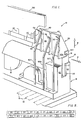
- Fig. 1 With reference to Fig. 1, it is to be understood that, for reasons of clarity of showing only, a detail of a single side only of one form of ZIF connector according to the present invention is shown and described, since the extension of the teaching to the omitted parts of the connector, having two facing rows of contacts defining a series of opposing contact wires which receive a printed circuit board therebetween, is direct.
- Contact wires 50 extend through a lower housing 14 into holes cut into a substrate 12.
- the walls of the holes in substrate 12 are plated with a conductive strip 13 which extends beyond lower housing 14 to establish contact between external electrical devices and contact wires 50.
- the contact wires are soldered to the holes in substrate 12.
- a linear cam 16 having cam lobes 18 on a bottom portion 17 is mounted for linear motion (in the direction of arrow A) along lower housing 14. More specifically, lower housing 14 has projections 22, 24 which define a guideway 26 therebetween. Bottom portion 17 of linear cam 16 is disposed within guideway 26. Lower housing 14 is further provided with a cam follower 28, a portion of which is disposed within guideway 26. Thus, when linear cam 16 is displaced horizontally within guideway 26, the cam followers 28 of lower housing 14 cams against the cam lobes 18 to impart a vertical displacement to linear cam 16.
- a cam carriage (hereinafter “upper housing”) 30 is mounted on the linear cam 16. Specifically, upper housing 30 is mounted for movement on a carriage guideway 19 defined by a hook-shaped member 19A projecting from the upper surface of linear cam 16. A C-shaped portion 30a of upper housing 30 loosely engages hook-shaped portion 19A to maintain upper housing 30 on carriage guideway 19. Note that the upper housing 30 is surrounded by lower housing 14, restricting the upper housing to vertical movement. For the sake of clarity, the portion of lower housing 14 which surrounds upper housing 30 is not shown. Note further that upper housing 30 comprises two facing sides (only one of which is shown in Fig. 1) defining an elongated slot through which the printed circuit board is inserted.
- a plurality of contact cams 40 are mounted on and project from the inwardly-facing surface 32 of upper housing 30.
- the contact cams 40 have distinct camming surface profiles 42, which will be described in more detail hereinafter.
- the contact cams 40 cam against contact wires 50.
- Contact wires 50 comprise cam-engaging portions 52 and end portions 54. End portions 54 of contact wires 50 establish an electrical contact with 1/0 pads 110 of printed circuit board 100.
- contact wires 50 project through lower housing 14 to communicate with external electrical conductors.
- contact wires 50 could communicate with conductors 13 printed on the surface of substrate 12.
- Contact wires 50 are of different lengths; that is, the contact wires along each row alternate between a first contact wire 50X of a length X and a second contact wire 50Y of a length Y as shown in Fig. 1.
- the contacts are arranged into two opposing rows (the other row is not shown in Fig. 1) such that a contact 50Y on one row is disposed opposite a contact 50X on the other row.
- the two rows of contacts can be thought of as a series of opposing contact pairs, where each " pair" has contact wires of lengths X and Y.
- the contact wires are mounted at varying angles with respect to the upper housing 30; that is, although the contact wires 50X are displaced by a distance W with respect to contact wires 50Y, the portions 52 of contacts 50X and 50Y are in alignment. This is done in order to vary the force with which the contacts engage the printed circuit boards.
- contact portion 54 wipes the surface of I/O pad 110 between point 3 and a point 4 thereof.
- the contact portion 54 is maintained in abutment at point 4 on 1/0 pad 110.
- the above described embodiment utilises a plurality of contact cams with spaces between each cam to cause the contact wires of a ZIF connector to complete a wipe cycle on the I/O pads of a printed circuit board, while, in Fig. 3, the same or similar contact cams are shown as being in abutment.
- the present invention encompasses both arrangements.
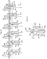
- Fig. 3 ten different contact cams are shown. Each contact cam has a different camming surface profile, as described in more detail below, the surface profiles of contact cams 3X and 3Y being shown in cross section in Fig. 4.
- the "LOW" portion of cam 3X in Fig. 3 corresponds to the profile area (or region) of the cam ("LOW" in Fig. 4) having a width A; region "A B" of cam 3X in Fig. 3 corresponds to the upward ramp AB of cam 3X of Fig.
- region "HIGH” of Fig. 3 corresponds to the profile region of the cam ("HIGH” in Fig. 4) having a constant width B; region “B C” in Fig 3 corresponds to the downward ramp BC in Fig. 4 having a width decreasing from width B to a width C; the region “WELL” of Fig. 3 corresponds to the profile region of the cam ("WELL” in Fig. 4) having a width C; the region “C D” in Fig. 3 corresponds to the upward ramp CD in Fig. 4 having a width increasing from width C to a width D; and the "MEDIUM" portion of cam 3X in Fig.
- FIG. 4 corresponds to the profile region of the cam ("MEDIUM” in Fig. 4) having a constant width D. Note that width D is less than width B (i.e., AOCODOB). Note further that cam regions B-C-D in Figs. 3 and 4 may have an arc-like (i.e., rounded) profile as shown in Fig. 2. Finally, note that the length of the regions in Fig. 3 corresponded to the portion of the contact cam which contains the given profile region shown in Fig. 4. For example, the length of region "HIGH" of cam 3X in Fig. 3 corresponds to the portion of the cam which has the profile region "HIGH” thereon (see Fig. 4).
- Fig. 3 shows a schematic view of the surface profiles of adjacent contact cams. Note that one difference between the surface profiles of adjacent contact cams is the length of the respective HIGH regions. That is, contact cams 5X and 5Y have longer HIGH regions than do contact cams 4X and 4Y, which have longer HIGH regions than contact cams 3X and 3Y, etc., down to the point where the HIGH region is extremely small in cams IX and IY. Another difference between the surface profiles of adjacent contact cams is that all of the "X" contact cams have LOW regions of a first length while all of the "Y" contact cams have LOW regions of a second length smaller than the first length.
- the above-described cam surface profiles are distributed along surface 32 of upper housing 30 in a specific pattern.
- the X cam types are disposed behind contact wires having a length X
- the Y cam types are disposed behind contact wires having a length Y (see Fig. 1).
- the profiles of the cams cause the wires to simultaneously abut the printed circuit board.
- the 1/0 pads 110 on PCB 100 are staggered. That is, the 1/0 pads which are contacted by wires 50X are disposed below those which are contacted by wires 50Y, forming two staggered, aligned rows of pads.
- contact wires 50Y originally contact 1/0 pads at a point A as shown, while contact wires 50X originally contact the pads at a point B.
- the staggering of the contact wires and the 1/0 pads is done in order to increase the number of contacts per unit area of the printed circuit board.
- Contact cams of the same variety e.g., 3X and 3Y
- the cams are of the same variety, they will cause the contact wires to perform similar wipe cycles. More specifically, as shown in Fig. 6, since the positions of the wires are different (or staggered), the wires will perform staggered wipe cycles.
- the stagger of the staggered wipe cycles is created by both the differing contact wire lengths as well as the different lengths of the "low" regions of the cams.
- the contact cams are disposed on two contact cam rows which are separated by a gap through which the printed circuit board is inserted.
- no two contact cams on each contact cam row are alike.
- Each row of cams consist of the five varieties of cams of both types, for a total of ten cams per row.
- the cams are distributed such that the first cam of the first row is the same as the tenth cam of the second row, the second cam of the first row is the same as the ninth cam of the second row, etc.
- the first row has a first cam group (5X-1X) and a second cam group (1Y-5Y)
- the second row has a corresponding first cam group (5Y-lY) and a second cam group (1X-5X).
- the groups differ by the types of the cams such that no two cams on a given row are the same.
- the above-described arrangement also achieves a balancing of forces which tends to promote the stability of the printed circuit board within the connector. For example, consider cams 5X and 4Y of Row 1 and cams 5Y and 4X of Row 2 (see Fig. 5). As previously discussed, the wipe cycles imparted by the contact wires (via cams 4X of Row 2 and 4Y of Row 1) are staggered. In addition, the wipe cycles imparted via contact cams 5X and contact cams 4Y of Row 1 would also be staggered. Thus, in addition to the staggering of wipe cycles imparted by opposing cams, the present invention provides staggered wipe cycles to adjacent contact wires on the same row.
- the rows of cams of the invention could have one, two, three, or more groups of cams.
- the specific composition of the groups of cams on each row may be varied.
- the contact wires (and the staggering of the I/O pads) could be altered such that there are wires of three or more different lengths.
- the arrangements described work just as well with only one row of contents.
- the present invention provides means by which the contact wires of a ZIF connector can be modified to perform staggered wipe cycles on one or both sides of a printed circuit board. This result is achieved in the embodiments selected for description through the provision of a camming mechanism which is of relatively simple construction. Moreover, since the entire assembly could be manufactured from any one of a number of known non-conductive materials such as thermosetting resins, etc-, this particular construction is relatively inexpensive to manufacture.
- a zero insertion force type printed circuit board edge connector for establishing electrical contact between a plurality of opposing contact pads disposed on both sides of an edge of a printed circuit board and a plurality of electrical conductors disposed on a base, comprising:
- first means mounted on the upper housing for moving the two opposing rows of contacts into simultaneous abutment with the plurality of opposing contact pads, the first means causing a majority of adjacent ones of the plurality of contacts on each of the opposing rows of contacts to perform sequential wipe cycles on respective adjacent ones of the plurality of opposing contact pads, and causing adjacent and opposing ones of the plurality of contacts to perform staggered wipe cycles on respective adjacent and opposing ones of the plurality of opposing contact pads,
- the first means comprising a plurality of cams arranged into two opposing rows of cams mounted on the upper housing on either side of the slot of the upper housing, each one of the plurality of cams abutting a respective one of the plurality of contacts.
- Each one of the plurality of cams has a first region of a first width, a second region of a second width greater than the first width, a third region of a third width greater than the first width and smaller than the second width, and a fourth region of a fourth width greater than the third width and less than the second width, the second regions of the plurality of cams have different lengths, the sequential wipe cycles of the plurality of contacts being defined by the length of the second regions of the plurality of cams, every other one of the plurality of contacts along each of the two opposing rows of contacts being of a first length, and the others of the plurality of contacts along each of the two opposing rows of contacts are of a second length greater than the first length.
- the lengths of the second region of a first one of the plurality of cams of each of the cam groups is of a fifth length, the second region of a second one of the plurality of cams of each of the cam groups being of a sixth length, the sixth length being less than the fifth length, the second region of a third one of the plurality of cams of.
- each of the cam groups being of a seventh length, the seventh length being less than the sixth length, the second region of a fourth one of the plurality of cams of each of the cam groups being of an eighth length, the eighth length being less than the seventh length, and the second region of a fifth one of the plurality of cams of each of the cam groups being of a ninth length, the ninth length being less than the eighth length.
Description
- The present invention relates to zero insertion force edge connectors for printed circuit boards (hereinafter ZIF connectors) having means for wiping the contacts of the connector against the I/O pads of the printed circuit board in order to ensure electrical contact therebetween.
- The use of connector blocks to establish electrical contact between the I/0 pads of a printed circuit board and external signal and/or power sources is well known in the art. A connector block typically comprises an outer housing of an electrically non-conductive material and a plurality of contact wires disposed within the housing. The contact wires are arranged into two opposing rows of contact pairs which engage the I/O pads disposed on opposite sides of the printed circuit board.
- In a conventional connector block, the spacing between the contact wire rows is set such that the wires immediately contact the printed circuit board upon insertion. This immediate contact produces a force opposing the further insertion of the printed circuit board into the connector block. Thus, as the number of I/O ports on the printed circuit board (and the number of contact wires) increases, it becomes increasingly difficult to insert the printed circuit board into the connector block. ZIF connectors overcome this difficulty by setting the spacing between the contact wire rows such that the wires do not immediately contact the printed circuit board. In such ZIF connectors, the contact wires are brought into abutment with the I/0 pads of the printed circuit board only after the board has been completely inserted into the connector.
- A problem which typically occurs in connector technology is the degradation of the electrical contact between the contact wires of the connector and the I/O pads of the printed circuit board. For example, this degradation can be produced by dust build-up on the I/O pads. In the above-described conventional connector blocks, this problem is inherently addressed. Specifically, as the printed circuit board is inserted between the contact wire rows, the wires frictionally engage the I/O pads to remove dust and/or other non-conductive debris. This so-called "wiping cycle" process has been quite satisfactory in greatly reducing contact degradation. However, since there is no frictional engagement between the I/O ports and the contact wires of a ZIF connector during the insertion of the printed circuit board into the connector, the above-described wiping cycle process cannot be used.
- Thus a need has arisen to modify ZIF connectors so that their contact wires can perform wiping cycles. In attempting to formulate the above-described modification, it was noticed that the stability of the printed circuit board within the was reduced by these wiping cycles, since the printed circuit board tended to move with the contact wires reducing or eliminating wiping. This problem is especially troublesome in connectors having a high number of contact wires, and where the weight of the printed circuit board is relatively low.
- U.S. Patent 4,189,200 (granted Feb. 19, 1980) to Yeager et al) discloses a ZIF connector. The contacts of the Yeager connector are sequentially cam-actuated, by power group, for engagement with an edge of a printed circuit board. More specifically, the contacts are actuated at different times by means of a cam and a drive member having a step profile. It is observed that, although this provision results in a verbal similarity to that which is claimed in the present document, it is for different purposes and would not solve the problems tackled thereby. With the arrangement of Yeager, the card would tip, if there were wipe with a sufficiently dense aggregation of contacts.
- U.S. Patent 4,266,839 (issued May 12, 1981 to Aikens) (=EP-A-0,022,305) discloses a sequentially actuated ZIF connector. A "toggle rod" is connected to the free ends of the contact wires. After the printed circuit board is inserted into the Aikens connector, the toggle rod is rotated, forcing the contact wires into sequential engagement with the 1/O pads of the printed circuit board. Subsequently, upon further rotation of the toggle rods, the contact wires move along the surface of o the I/0 pads completing a wiping cycle thereon.
- U.S. Patent 4,076,362 (issued Feb. 28, 1978 to Ichimura) discloses a ZIF connector having means for sequentially engaging the 1/O pads of a printed circuit board. A slider is slideable longitudinally along the connector. The slider has a channel cut therein which communicates with a projection from a cam member abutting a contact wire. As the slider slides past the cam member, the cam member projection engages the channel of the slider, causing the cam member to move upward. The cam surface of the cam member engages the contact wire, forcing the contact wire inwardly to engage the printed circuit board. At best, this provides a most unsatisfactory solution to the presently tackled problem.
- As described above, the art shows sequential actuation of ZIF connector contacts. Moreover, the art also teaches the use of a wiping cycle to clean the I/O pads of the printed circuit board inserted into a ZIF connector. However, what the art does not show is a satisfactory solution to the worst case problem, which is the usual problem, of securing a satisfactory wipe when a single card of no specialised structure is engaged by a ZIF connector on one edge only, but from both sides thereof, such solution also meeting the milder versions of the problem.
- Accordingly the present invention provides a ZIF connector having a dense array of contacts actuated by a common actuator in such a way as to bring all the contacts into engagement with an inserted board at the same time and, thereafter, to generate individual wipe cycles for each contact, so arranged that, for a single engagement in which all contacts wipe once if there exists a pad for them to wipe against, wiping is performed by sequential groups of contacts, each group being spread evenly across the array of contacts. The effect of this arrangement is to grip the board by means of the majority of the contacts over all of its width while generating wipe at spaced positions across its width, promoting the stability of the printed circuit board within the connector without the use of external support structures.
- As particularly described hereinafter, this is achieved economically in a worst case connector by the provision of a contact actuating member which abuts the contact wires of a zero input force connector. The contact-actuating member comprises an upper housing mounted on a moveable linear cam. The horizontal displacement of the linear cam imparts a vertical displacement to the upper housing. The upper housing has a plurality of contact cams thereon. The contact cams are arranged in a single row (or two facing rows) disposed behind the contact wires such that each contact cam abuts one of the contact wires of the connector. The surface profiles of the contact cams are constructed such that the contact wires contact the I/O ports on opposite sides of the printed circuit board, and then perform sequential wipe cycles on the 1/0 pads at different points thereon (i.e., producing staggered wipe cycles).
- A feature of the described arrangement is the surface profiles of the contact cams. Opposing contact cams (i.e., contact cams at the same position along the opposing contact cam rows) have staggered surface profiles. Furthermore, the surface profiles of adjacent contact cams are also staggered. Thus, any given contact cam has a surface profile which is different from (i.e., relatively staggered with respect to) the surface profiles of both its opposite and the immediately adjacent contact cams. This feature promotes the stability of the printed circuit board within the connector by producing staggered wipe cycles (i.e., the cycles of both the opposite and the immediately adjacent contact wires produce forces which tend to oppose each other). Moreover, the surface profiles are constructed such that adjacent contact wires perform sequential wipe cycles.
- The present invention will be described further by way of example with reference to an embodiment thereof as illustrated in the accompanying drawings, in which:
- Fig. 1 is a cut-away view of a detail of one embodiment of the invention;
- Fig. 2, in sections A-F, is a diagrammatic illustration of the wipe cycle of a typical one of the contacts of the embodiment of Fig. 1;
- Fig. 3 is a frontal view of the contact cams of the embodiment of Fig. 1;
- Fig. 4 is a side view of two adjacent contact cams of the of the embodiment of Fig. 1;
- Fig. 5 is an explanatory diagram illustrating the relative positions of the contact cams along opposing contact cam rows; and
- Fig. 6 is a side view of a selected pair of opposing contacts engaging a printed circuit board therebetween.
- With reference to Fig. 1, it is to be understood that, for reasons of clarity of showing only, a detail of a single side only of one form of ZIF connector according to the present invention is shown and described, since the extension of the teaching to the omitted parts of the connector, having two facing rows of contacts defining a series of opposing contact wires which receive a printed circuit board therebetween, is direct.
- Contact
wires 50 extend through alower housing 14 into holes cut into asubstrate 12. The walls of the holes insubstrate 12 are plated with aconductive strip 13 which extends beyondlower housing 14 to establish contact between external electrical devices andcontact wires 50. The contact wires are soldered to the holes insubstrate 12. - A
linear cam 16 havingcam lobes 18 on abottom portion 17 is mounted for linear motion (in the direction of arrow A) alonglower housing 14. More specifically,lower housing 14 hasprojections 22, 24 which define aguideway 26 therebetween.Bottom portion 17 oflinear cam 16 is disposed withinguideway 26.Lower housing 14 is further provided with acam follower 28, a portion of which is disposed withinguideway 26. Thus, whenlinear cam 16 is displaced horizontally withinguideway 26, thecam followers 28 oflower housing 14 cams against thecam lobes 18 to impart a vertical displacement tolinear cam 16. - A cam carriage (hereinafter "upper housing") 30 is mounted on the
linear cam 16. Specifically,upper housing 30 is mounted for movement on acarriage guideway 19 defined by a hook-shapedmember 19A projecting from the upper surface oflinear cam 16. A C-shaped portion 30a ofupper housing 30 loosely engages hook-shapedportion 19A to maintainupper housing 30 oncarriage guideway 19. Note that theupper housing 30 is surrounded bylower housing 14, restricting the upper housing to vertical movement. For the sake of clarity, the portion oflower housing 14 which surroundsupper housing 30 is not shown. Note further thatupper housing 30 comprises two facing sides (only one of which is shown in Fig. 1) defining an elongated slot through which the printed circuit board is inserted. - A plurality of
contact cams 40 are mounted on and project from the inwardly-facingsurface 32 ofupper housing 30. Thecontact cams 40 have distinct camming surface profiles 42, which will be described in more detail hereinafter. Thecontact cams 40 cam againstcontact wires 50.Contact wires 50 comprise cam-engagingportions 52 andend portions 54.End portions 54 ofcontact wires 50 establish an electrical contact with 1/0pads 110 of printedcircuit board 100. Note thatcontact wires 50 project throughlower housing 14 to communicate with external electrical conductors. For example,contact wires 50 could communicate withconductors 13 printed on the surface ofsubstrate 12.Contact wires 50 are of different lengths; that is, the contact wires along each row alternate between afirst contact wire 50X of a length X and asecond contact wire 50Y of a length Y as shown in Fig. 1. - The contacts are arranged into two opposing rows (the other row is not shown in Fig. 1) such that a
contact 50Y on one row is disposed opposite acontact 50X on the other row. Thus, the two rows of contacts can be thought of as a series of opposing contact pairs, where each " pair" has contact wires of lengths X and Y. The contact wires are mounted at varying angles with respect to theupper housing 30; that is, although thecontact wires 50X are displaced by a distance W with respect tocontact wires 50Y, theportions 52 ofcontacts - The general operation of the connector of the invention will now be described with reference to Figs. 1 and 2A-2F. When
linear cam 16 is in the position as shown in Fig. 1,portion 52 of acontact wire 50 engages the uppermost portion of acontact cam 40. As shown in Fig. 2A, the contact wire abutscontact cam 40 at its lowest surface AA. At this point, the contact wires are maintained at a position removed from I/O pads 110 of printedcircuit board 100. As thelinear cam 16 is moved horizontally (i.e., in the direction of arrow A) thecam follower 28 cams against thecam rods 18, imparting a vertical motion (in the direction of arrow B) to theupper housing 30. Thus, as shown in Figs. 2B-2F, thecontact cam 40 moves in an upward direction. - As shown in Fig. 2B, as the
wire portion 52 abuts an upward ramp portion AB ofcontact cam 40,wire portion 54 is brought into contact with I/O pad 110 at a point 1. Aswire portion 52 moves up ramp AB,contact portion 54 wipes the surface of the I/O pad 110 between point 1 and a point 2. As shown in Figs. 2C and 2D, cam surface BB maintains thecontact portion 54 at point 2 on I/O pad 110. As shown in Fig. 2E, when thecam portion 52 abuts downward-sloping trough surface BC ofcontact cam 40, thecontact portion 54 wipes the surface of the I/O pad 110 between point 2 and a point 3 thereon. Ascam portion 52 abuts upward-sloping trough surface CD,contact portion 54 wipes the surface of I/O pad 110 between point 3 and a point 4 thereof. Finally, as shown in Fig. 2F, as thecam portion 52 abuts surface DD ofcontact cam 40, thecontact portion 54 is maintained in abutment at point 4 on 1/0pad 110. - The above described embodiment utilises a plurality of contact cams with spaces between each cam to cause the contact wires of a ZIF connector to complete a wipe cycle on the I/O pads of a printed circuit board, while, in Fig. 3, the same or similar contact cams are shown as being in abutment. The present invention encompasses both arrangements.
- In Fig. 3, ten different contact cams are shown. Each contact cam has a different camming surface profile, as described in more detail below, the surface profiles of
contact cams cam 3X in Fig. 4 and the frontal view ofcam 3X in Fig. 3 will facilitate our discussion. As it is apparent upon comparison, the "LOW" portion ofcam 3X in Fig. 3 corresponds to the profile area (or region) of the cam ("LOW" in Fig. 4) having a width A; region "A B" ofcam 3X in Fig. 3 corresponds to the upward ramp AB ofcam 3X of Fig. 4 having a width increasing from width A to a width B; region "HIGH" of Fig. 3 corresponds to the profile region of the cam ("HIGH" in Fig. 4) having a constant width B; region "B C" in Fig 3 corresponds to the downward ramp BC in Fig. 4 having a width decreasing from width B to a width C; the region "WELL" of Fig. 3 corresponds to the profile region of the cam ("WELL" in Fig. 4) having a width C; the region "C D" in Fig. 3 corresponds to the upward ramp CD in Fig. 4 having a width increasing from width C to a width D; and the "MEDIUM" portion ofcam 3X in Fig. 4 corresponds to the profile region of the cam ("MEDIUM" in Fig. 4) having a constant width D. Note that width D is less than width B (i.e., AOCODOB). Note further that cam regions B-C-D in Figs. 3 and 4 may have an arc-like (i.e., rounded) profile as shown in Fig. 2. Finally, note that the length of the regions in Fig. 3 corresponded to the portion of the contact cam which contains the given profile region shown in Fig. 4. For example, the length of region "HIGH" ofcam 3X in Fig. 3 corresponds to the portion of the cam which has the profile region "HIGH" thereon (see Fig. 4). - As is now apparent in view of the above discussion, Fig. 3 shows a schematic view of the surface profiles of adjacent contact cams. Note that one difference between the surface profiles of adjacent contact cams is the length of the respective HIGH regions. That is,
contact cams cams contact cams - As shown in Fig. 3, the above-described cam surface profiles are distributed along
surface 32 ofupper housing 30 in a specific pattern. First, the X cam types are disposed behind contact wires having a length X, and the Y cam types are disposed behind contact wires having a length Y (see Fig. 1). Thus, even though the contact wires are of different lengths, the profiles of the cams cause the wires to simultaneously abut the printed circuit board. Further, note that the 1/0pads 110 onPCB 100 are staggered. That is, the 1/0 pads which are contacted bywires 50X are disposed below those which are contacted bywires 50Y, forming two staggered, aligned rows of pads. For example, with reference to Fig. 6,contact wires 50Y originally contact 1/0 pads at a point A as shown, whilecontact wires 50X originally contact the pads at a point B. The staggering of the contact wires and the 1/0 pads is done in order to increase the number of contacts per unit area of the printed circuit board. Contact cams of the same variety (e.g., 3X and 3Y) are disposed relatively opposite of each other to form opposing contact cam pairs. Since the cams are of the same variety, they will cause the contact wires to perform similar wipe cycles. More specifically, as shown in Fig. 6, since the positions of the wires are different (or staggered), the wires will perform staggered wipe cycles. Thus, the stagger of the staggered wipe cycles is created by both the differing contact wire lengths as well as the different lengths of the "low" regions of the cams. - With reference to Fig. 5, the contact cams are disposed on two contact cam rows which are separated by a gap through which the printed circuit board is inserted. Thus, no two contact cams on each contact cam row are alike. Each row of cams consist of the five varieties of cams of both types, for a total of ten cams per row. The cams are distributed such that the first cam of the first row is the same as the tenth cam of the second row, the second cam of the first row is the same as the ninth cam of the second row, etc. Thus, the first row has a first cam group (5X-1X) and a second cam group (1Y-5Y), the second row has a corresponding first cam group (5Y-lY) and a second cam group (1X-5X). The groups differ by the types of the cams such that no two cams on a given row are the same.
- This arrangement results in causing a majority of the contact wires to perform sequential wipe cycles. As previously discussed, all of the contact wires are simultaneously brought into contact with the printed circuit board. Thereafter, due to the differing HIGH region lengths, contact wires abutting contact cams 1X and 1Y will complete their wipe cycles prior to those abutting
contact cams contact cams - The above-described arrangement also achieves a balancing of forces which tends to promote the stability of the printed circuit board within the connector. For example, consider
cams cams cams 4X ofRow 2 and 4Y of Row 1) are staggered. In addition, the wipe cycles imparted viacontact cams 5X andcontact cams 4Y of Row 1 would also be staggered. Thus, in addition to the staggering of wipe cycles imparted by opposing cams, the present invention provides staggered wipe cycles to adjacent contact wires on the same row. It is to be noted that the rows of cams of the invention could have one, two, three, or more groups of cams. The specific composition of the groups of cams on each row may be varied. Further, the contact wires (and the staggering of the I/O pads) could be altered such that there are wires of three or more different lengths. Moreover, as previously stated, the arrangements described work just as well with only one row of contents. - In summary, the present invention provides means by which the contact wires of a ZIF connector can be modified to perform staggered wipe cycles on one or both sides of a printed circuit board. This result is achieved in the embodiments selected for description through the provision of a camming mechanism which is of relatively simple construction. Moreover, since the entire assembly could be manufactured from any one of a number of known non-conductive materials such as thermosetting resins, etc-, this particular construction is relatively inexpensive to manufacture.
- There has been described a zero insertion force type printed circuit board edge connector for establishing electrical contact between a plurality of opposing contact pads disposed on both sides of an edge of a printed circuit board and a plurality of electrical conductors disposed on a base, comprising:
- a lower housing mounted on the base, the lower housing defining a guideway having a plurality of upward-facing cam followers;
- a slider mounted for horizontal movement along the guideway of the lower housing, the slider having a plurality of downward-facing cam lobes;
- an upper housing mounted on the slider, the upper housing having an opening for receiving the edge of the printed circuit board;
- a plurality of contacts connected through the lower housing to the plurality of electrical conductors, the plurality of contacts being arranged into two opposing rows of contacts disposed within the opening in the upper housing, the two opposing rows of contacts being substantially parallel to one another; and
- first means mounted on the upper housing for moving the two opposing rows of contacts into simultaneous abutment with the plurality of opposing contact pads, the first means causing a majority of adjacent ones of the plurality of contacts on each of the opposing rows of contacts to perform sequential wipe cycles on respective adjacent ones of the plurality of opposing contact pads, and causing adjacent and opposing ones of the plurality of contacts to perform staggered wipe cycles on respective adjacent and opposing ones of the plurality of opposing contact pads,
- the first means comprising a plurality of cams arranged into two opposing rows of cams mounted on the upper housing on either side of the slot of the upper housing, each one of the plurality of cams abutting a respective one of the plurality of contacts.
- Each one of the plurality of cams has a first region of a first width, a second region of a second width greater than the first width, a third region of a third width greater than the first width and smaller than the second width, and a fourth region of a fourth width greater than the third width and less than the second width, the second regions of the plurality of cams have different lengths, the sequential wipe cycles of the plurality of contacts being defined by the length of the second regions of the plurality of cams, every other one of the plurality of contacts along each of the two opposing rows of contacts being of a first length, and the others of the plurality of contacts along each of the two opposing rows of contacts are of a second length greater than the first length. The lengths of the second region of a first one of the plurality of cams of each of the cam groups is of a fifth length, the second region of a second one of the plurality of cams of each of the cam groups being of a sixth length, the sixth length being less than the fifth length, the second region of a third one of the plurality of cams of. each of the cam groups being of a seventh length, the seventh length being less than the sixth length, the second region of a fourth one of the plurality of cams of each of the cam groups being of an eighth length, the eighth length being less than the seventh length, and the second region of a fifth one of the plurality of cams of each of the cam groups being of a ninth length, the ninth length being less than the eighth length.
- In other words, in each of the two opposing rows of cams there occur, in sequential order, the first one of the plurality of cams, the second one of the plurality of cams, the third one of the plurality of cams, the fourth one of the plurality of cams, the fifth one of the plurality of cams, the fifth one of the plurality of cams, the fourth one of the plurality of cams, the third one of the plurality of cams, the second one of the plurality of cams, and the first one of the plurality of cams, the first regions of adjacent ones of the plurality of cams alternating between a third length and a fourth length greater than the third length, and wherein contacts of the first length abut respective ones of the cams having the first regions of the third length, each of the plurality of cams having the first regions of the third length being disposed immediately opposite from respective ones of the plurality of cams having the first regions of the fourth length.
- While the invention has been shown and described with reference to selected embodiments thereof, it will be understood by those skilled in the art that modifications to the arrangements disclosed herein may be made without departing from the scope of the appended claims.
Claims (10)
Applications Claiming Priority (2)
| Application Number | Priority Date | Filing Date | Title |
|---|---|---|---|
| US06/581,529 US4542950A (en) | 1984-02-21 | 1984-02-21 | Zero insertion force edge connector with wipe cycle |
| US581529 | 1984-02-21 |
Publications (3)
| Publication Number | Publication Date |
|---|---|
| EP0152566A2 EP0152566A2 (en) | 1985-08-28 |
| EP0152566A3 EP0152566A3 (en) | 1987-02-04 |
| EP0152566B1 true EP0152566B1 (en) | 1989-04-05 |
Family
ID=24325547
Family Applications (1)
| Application Number | Title | Priority Date | Filing Date |
|---|---|---|---|
| EP84114668A Expired EP0152566B1 (en) | 1984-02-21 | 1984-12-04 | Zero insertion force edge connectors |
Country Status (4)
| Country | Link |
|---|---|
| US (1) | US4542950A (en) |
| EP (1) | EP0152566B1 (en) |
| JP (1) | JPS60189881A (en) |
| DE (1) | DE3477625D1 (en) |
Families Citing this family (21)
| Publication number | Priority date | Publication date | Assignee | Title |
|---|---|---|---|---|
| US4684194A (en) * | 1984-07-16 | 1987-08-04 | Trw Inc. | Zero insertion force connector |
| US4705338A (en) * | 1985-12-13 | 1987-11-10 | E. I. Du Pont De Nemours And Company | Zero insertion force connector |
| JPS62276773A (en) * | 1986-05-23 | 1987-12-01 | 住友電気工業株式会社 | Connection of flexible printed circuit and connector |
| US4863395A (en) * | 1989-01-17 | 1989-09-05 | Robert Babuka | Zero insertion force connector with component card |
| US4975074A (en) * | 1989-02-24 | 1990-12-04 | Cray Research, Inc. | Cam actuated electrical connector |
| US4872851A (en) * | 1989-02-27 | 1989-10-10 | International Business Machines Corp. | Electrical connector with torsional contacts |
| US4919626A (en) * | 1989-04-14 | 1990-04-24 | Itt Corporation | Connector for IC card |
| US4984993A (en) * | 1989-05-12 | 1991-01-15 | Cray Research, Inc. | Two-piece edge ZIF connector with sliding block |
| US4951425A (en) * | 1989-11-02 | 1990-08-28 | Herschel Naghi | Computer and video game cleaning cartridge |
| US5243730A (en) * | 1989-12-13 | 1993-09-14 | Nintendo Of America Inc. | Apparatus for cleaning electronic game consoles and cartridges |
| US5025526A (en) * | 1989-12-13 | 1991-06-25 | Nintendo Of America, Inc. | Apparatus for cleaning electronic game consoles and cartridges |
| SG43825A1 (en) * | 1991-08-05 | 1997-11-14 | Molex Inc | Card edge connector assembly |
| US5316496A (en) * | 1992-02-28 | 1994-05-31 | The Whitaker Corporation | Connector for flat cables |
| US5813876A (en) * | 1996-06-13 | 1998-09-29 | Intel Corporation | Pressure actuated zero insertion force circuit board edge connector socket |
| US5807126A (en) * | 1996-11-05 | 1998-09-15 | Itt Industries, Inc. | Low profile connector system |
| US6257911B1 (en) | 1999-11-10 | 2001-07-10 | Frank S. Shelby | Low insertion force connector with wipe |
| US6672891B2 (en) * | 2001-09-28 | 2004-01-06 | Intel Corporation | Zero insertion force connector for substrates with edge contacts |
| DE10302138A1 (en) * | 2002-02-19 | 2003-08-21 | Tyco Electronics Amp Gmbh | Pluggable connector, uses plug element with two slide-ways one of which is taken back relative to other |
| KR100807469B1 (en) | 2006-11-29 | 2008-02-25 | 삼성전기주식회사 | Zif connector type board and testing method of the same |
| DE102008046767B4 (en) * | 2008-09-11 | 2020-03-26 | Valeo Schalter Und Sensoren Gmbh | Contacting device |
| WO2016018709A1 (en) * | 2014-07-29 | 2016-02-04 | 3M Innovative Properties Company | Multiple row connector with zero insertion force |
Family Cites Families (9)
| Publication number | Priority date | Publication date | Assignee | Title |
|---|---|---|---|---|
| US4076362A (en) * | 1976-02-20 | 1978-02-28 | Japan Aviation Electronics Industry Ltd. | Contact driver |
| US4189200A (en) * | 1977-11-14 | 1980-02-19 | Amp Incorporated | Sequentially actuated zero insertion force printed circuit board connector |
| US4178053A (en) * | 1978-02-13 | 1979-12-11 | Ncr Corporation | Zero-insertion force electrical connector |
| US4270826A (en) * | 1979-02-01 | 1981-06-02 | Thomas & Betts Corporation | Zero insertion force connector |
| US4266839A (en) * | 1979-07-06 | 1981-05-12 | E. I. Du Pont De Nemours And Company | Zero insertion force toggle link connector |
| US4357066A (en) * | 1980-05-27 | 1982-11-02 | Ford Motor Company | Printed circuit board edge terminal |
| JPS5722712U (en) * | 1980-07-11 | 1982-02-05 | ||
| US4428635A (en) * | 1982-02-24 | 1984-01-31 | Amp Incorporated | One piece zif connector |
| US4480884A (en) * | 1983-07-01 | 1984-11-06 | International Business Machines Corporation | Zero insertion force connector and circuit card assembly |
-
1984
- 1984-02-21 US US06/581,529 patent/US4542950A/en not_active Expired - Lifetime
- 1984-12-04 DE DE8484114668T patent/DE3477625D1/en not_active Expired
- 1984-12-04 EP EP84114668A patent/EP0152566B1/en not_active Expired
- 1984-12-19 JP JP59266575A patent/JPS60189881A/en active Granted
Also Published As
| Publication number | Publication date |
|---|---|
| JPH0237665B2 (en) | 1990-08-27 |
| EP0152566A3 (en) | 1987-02-04 |
| JPS60189881A (en) | 1985-09-27 |
| EP0152566A2 (en) | 1985-08-28 |
| US4542950A (en) | 1985-09-24 |
| DE3477625D1 (en) | 1989-05-11 |
Similar Documents
| Publication | Publication Date | Title |
|---|---|---|
| EP0152566B1 (en) | Zero insertion force edge connectors | |
| EP0524248B1 (en) | Solder-bearing lead | |
| CN1126199C (en) | Electric connector with paired terminals | |
| EP0278868B1 (en) | Multi row high density connector | |
| US4428635A (en) | One piece zif connector | |
| US4705338A (en) | Zero insertion force connector | |
| CN1059985C (en) | Electrical connector with improved contact retention | |
| US4606594A (en) | ZIF connector with wipe | |
| US5533907A (en) | Electronic module socket with self-cleaning shorting contacts | |
| US4602834A (en) | Electrical jumper | |
| CN1592000A (en) | Bridge plug for electrical connection and/or terminal and electrical connection and/or terminal | |
| CN1134863C (en) | Appliance connector and production method thereof | |
| US4504101A (en) | Low insertion force connection arrangement | |
| US3990761A (en) | Zero force connector assembly | |
| US5951321A (en) | Multipin connector assembly | |
| DE1765978B1 (en) | CIRCUIT BLOCK FOR ELECTRICAL CONNECTION USING PLUG CONNECTIONS OF ELECTRICAL CIRCUIT ELEMENTS | |
| JPS622434B2 (en) | ||
| US4818241A (en) | Electrical interconnection device using elastomeric strips | |
| US4065200A (en) | Mounting rack for circuit panels | |
| WO1999044260A1 (en) | Contact strip for connecting two circuit boards and a process for producing the contact strip | |
| JPS6127074A (en) | Electric connector | |
| EP0236860A3 (en) | Connector for flat cable termination | |
| GB2167912A (en) | Electrical connector for flat multiconductor cable | |
| US4257660A (en) | Electric connector having a plurality of in-line contacts | |
| US3243762A (en) | Printed circuit connector |
Legal Events
| Date | Code | Title | Description |
|---|---|---|---|
| PUAI | Public reference made under article 153(3) epc to a published international application that has entered the european phase |
Free format text: ORIGINAL CODE: 0009012 |
|
| AK | Designated contracting states |
Designated state(s): DE FR GB |
|
| 17P | Request for examination filed |
Effective date: 19851213 |
|
| PUAL | Search report despatched |
Free format text: ORIGINAL CODE: 0009013 |
|
| AK | Designated contracting states |
Kind code of ref document: A3 Designated state(s): DE FR GB |
|
| 17Q | First examination report despatched |
Effective date: 19880624 |
|
| GRAA | (expected) grant |
Free format text: ORIGINAL CODE: 0009210 |
|
| AK | Designated contracting states |
Kind code of ref document: B1 Designated state(s): DE FR GB |
|
| REF | Corresponds to: |
Ref document number: 3477625 Country of ref document: DE Date of ref document: 19890511 |
|
| ET | Fr: translation filed | ||
| PLBE | No opposition filed within time limit |
Free format text: ORIGINAL CODE: 0009261 |
|
| STAA | Information on the status of an ep patent application or granted ep patent |
Free format text: STATUS: NO OPPOSITION FILED WITHIN TIME LIMIT |
|
| 26N | No opposition filed | ||
| PGFP | Annual fee paid to national office [announced via postgrant information from national office to epo] |
Ref country code: FR Payment date: 19961211 Year of fee payment: 13 |
|
| PG25 | Lapsed in a contracting state [announced via postgrant information from national office to epo] |
Ref country code: FR Free format text: THE PATENT HAS BEEN ANNULLED BY A DECISION OF A NATIONAL AUTHORITY Effective date: 19971231 |
|
| REG | Reference to a national code |
Ref country code: FR Ref legal event code: ST |
|
| PGFP | Annual fee paid to national office [announced via postgrant information from national office to epo] |
Ref country code: GB Payment date: 19991122 Year of fee payment: 16 |
|
| PG25 | Lapsed in a contracting state [announced via postgrant information from national office to epo] |
Ref country code: GB Free format text: LAPSE BECAUSE OF NON-PAYMENT OF DUE FEES Effective date: 20001204 |
|
| GBPC | Gb: european patent ceased through non-payment of renewal fee |
Effective date: 20001204 |
|
| PGFP | Annual fee paid to national office [announced via postgrant information from national office to epo] |
Ref country code: DE Payment date: 20011211 Year of fee payment: 18 |
|
| PG25 | Lapsed in a contracting state [announced via postgrant information from national office to epo] |
Ref country code: DE Free format text: LAPSE BECAUSE OF NON-PAYMENT OF DUE FEES Effective date: 20030701 |