EP0151726A2 - A shield for decoupling RF and gradient coils in an NMR apparatus - Google Patents
A shield for decoupling RF and gradient coils in an NMR apparatus Download PDFInfo
- Publication number
- EP0151726A2 EP0151726A2 EP84114885A EP84114885A EP0151726A2 EP 0151726 A2 EP0151726 A2 EP 0151726A2 EP 84114885 A EP84114885 A EP 84114885A EP 84114885 A EP84114885 A EP 84114885A EP 0151726 A2 EP0151726 A2 EP 0151726A2
- Authority
- EP
- European Patent Office
- Prior art keywords
- conductive regions
- array
- coil
- shield
- magnetic field
- Prior art date
- Legal status (The legal status is an assumption and is not a legal conclusion. Google has not performed a legal analysis and makes no representation as to the accuracy of the status listed.)
- Granted
Links
Images

Classifications
-
- G—PHYSICS
- G01—MEASURING; TESTING
- G01R—MEASURING ELECTRIC VARIABLES; MEASURING MAGNETIC VARIABLES
- G01R33/00—Arrangements or instruments for measuring magnetic variables
- G01R33/20—Arrangements or instruments for measuring magnetic variables involving magnetic resonance
- G01R33/28—Details of apparatus provided for in groups G01R33/44 - G01R33/64
- G01R33/42—Screening
- G01R33/422—Screening of the radio frequency field
-
- G—PHYSICS
- G01—MEASURING; TESTING
- G01R—MEASURING ELECTRIC VARIABLES; MEASURING MAGNETIC VARIABLES
- G01R33/00—Arrangements or instruments for measuring magnetic variables
- G01R33/20—Arrangements or instruments for measuring magnetic variables involving magnetic resonance
- G01R33/28—Details of apparatus provided for in groups G01R33/44 - G01R33/64
- G01R33/42—Screening
-
- Y—GENERAL TAGGING OF NEW TECHNOLOGICAL DEVELOPMENTS; GENERAL TAGGING OF CROSS-SECTIONAL TECHNOLOGIES SPANNING OVER SEVERAL SECTIONS OF THE IPC; TECHNICAL SUBJECTS COVERED BY FORMER USPC CROSS-REFERENCE ART COLLECTIONS [XRACs] AND DIGESTS
- Y10—TECHNICAL SUBJECTS COVERED BY FORMER USPC
- Y10S—TECHNICAL SUBJECTS COVERED BY FORMER USPC CROSS-REFERENCE ART COLLECTIONS [XRACs] AND DIGESTS
- Y10S505/00—Superconductor technology: apparatus, material, process
- Y10S505/825—Apparatus per se, device per se, or process of making or operating same
- Y10S505/842—Measuring and testing
- Y10S505/843—Electrical
- Y10S505/844—Nuclear magnetic resonance, NMR, system or device
Definitions
- This invention relates to nuclear magnetic resonance (NMR) apparatus. More specifically, the invention relates to decoupling shields particularly useful in an NMR apparatus for decoupling radio-frequency (RF) and gradient coils.
- NMR nuclear magnetic resonance
- RF radio-frequency
- the NMR apparatus includes a main magnet typically configured as a solenoid having a bore formed therein for accepting the NMR sample to be studied.
- the magnet which is frequently of a resistive or superconductive design is used to produce a homogeneous polarizing magnetic field in a predetermined region within the bore.
- the magnetic field is needed to polarize the nuclei within the sample, so that the NMR phenomenon can be excited.
- Magnetic fields utilized in NMR imaging and particularly those needed for in-vivo spectroscopy must be highly homogeneous to, for example, in excess of one part in a million.
- auxiliary field-correcting coils referred to as shim coils are provided in the magnet bore to provide the necessary correction factors.
- Radio-frequency coils constructed on cylindrical forms are positioned within the magnet bore coaxially with the longitudinal bore axis.
- the RF coils are used to irradiate the sample studied to excite the nuclear spins.
- the excited nuclei Upon cessation of the RF excitation, the excited nuclei radiate an NMR signal which is detected with the same coil used to excite the resonance or with a separate coil orthogonally oriented with respect to the excitation coil.
- three sets of gradient coils are provided within the bore.
- the gradient coils when energized are capable of producing three orthogonal, substantially linear magnetic field gradients each oriented along one of the directions of a conventional Cartesian coordinate system.
- the gradients are utilized in a well-known manner to encode into NMR signal spatial information of the nuclear spin distribution within the sample region excited by the RF coils. This information can be used to reconstruct images displaying one or more NMR parameters.
- the RF, gradient, and/or magnet shim coils are therefore situated in close proximity to one another.
- the RF coils are placed coaxially within the gradient coils.
- the gradient coils or shim coils can cause losses to occur in the RF coils. These losses can lower the quality factor Q of the RF coil resulting in a lower signal-to-noise ratio in the image.
- the signal-to-noise ratio can be improved by signal averaging, this is not a desirable solution since the NMR data collection time is unacceptably increased.
- the numerous windings within the gradient coils are coupled together by stray capacitances which can give rise to a plurality of spurious resonances when the RF coils are energized. If one or more of these spurious resonances interacts with the RF coil, the desired RF frequency may be displaced and the desired resonance damped. These detrimental effects increase with the proximity of the RF coils to the gradient coils.
- the interaction between the RF and gradient coils can be reduced or eliminated by placing an RF opaque screen between the gradient and RF coil forms.
- the screen must be several RF skin-depths thick to decouple the coils effectively.
- Suitable screens have been fashioned from copper mesh screen or copper foil having a thickness of .004 inches with a fiber backing. Such screens have been found effective in destroying RF interaction between the RF and gradient coils.
- a drawback associated with such simple shields is that the high-frequency response of the gradient coils is degraded.
- the rise time of the switched gradient field is lengthened by the eddy current induced in the continuous conductive layer of the RF shield.
- an object of the invention to provide an RF shield for effectively decoupling the RF and gradient coils without significantly degrading coil performance.
- An NIR apparatus includes means for producing a homogeneous magnetic field, a radio-frequency (RF) coil for transmitting and receiving RF energy, and gradient coils for generating pulsed linear magnetic field gradients at audio frequencies.
- a decoupling shield disposed between the RF and gradient coils is made up of first and second arrays of electrically conductive regions separated by relatively narrow non-conductive regions. The arrays are disposed on opposite surfaces of a member formed of a high dielectric material, and are offset relative to one another such that the conductive regions of the one array bridge the non-conductive regions of the other array to form a plurality of capacitive elements. In operation, the capacitive elements act essentially as electrical short circuits at radio frequencies and transmit substantially unaffected the homogeneous magnetic field and audio frequencies associated with the pulsed magnetic field gradients.
- FIGURE 1 depicts a side cross-sectional view of a superconductive K q R magnet generally designated 10.
- the magnet is of a solenoidal construction having a cylindrical bore 12 centered about a longitudinal axis 14.
- the magnet is provided with a set of main coil windings 16 which when energized produced the polarizing magnetic field.
- the main coils are disposed within a cryostat 18 containing suitable cryogens, such as liquid helium and nitrogen for maintaining the coil windings at superconductive temperatures characteristic of the materials used in the coils.
- One or more sets of shim coils 20 which may be of resistive or superconductive design are typically provided to correct for magnetic field inhomogeneities inherent in the main coil windings.
- Superconductive shim coils would, of course, be housed within cryostat 18. Shim coils of resistive or superconductive design are advantageously placed adjacent to the main coil windings.
- An RF coil assembly 22 is positioned coaxially inside a gradient coil assembly 24.
- An RF decoupling shield 26 is positioned coaxially between the RF and gradient coil assemblies.
- a region of the patient (not shown) to be examined is aligned with a generally spherical volume 28 where the polarizing and RF magnetic fields are homogeneous and where the gradient magnetic field produced by the gradient coil assemblies are linear.
- the shield is made up of two sheets 32 and 34 of a conductive material, such as copper, separated by a thin layer 36 of a low-loss flexible dielectric material such as Teflon synthetic resin polymer or polyethelene thermo-plastic polymer.
- the shield is constructed utilizing a double-sided copper-clad Teflon resin printed circuit board.
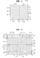
- Each of copper layers 32 and 34 is divided into an array of square or rectangular conductive areas (such as shaded areas designated 38) by etching (using conventional techniques) mutually perpendicular non-conductive gaps such as those designated in FIG. 2 by orthogonal lines 40 and 42.
- the pattern (depicted by dashed lines) on copper sheet 34 is offset with respect to the pattern (depicted by solid lines) on sheet 32 by one half the width of rectangular areas 38.
- the size of each array element 38 is made sufficiently small to minimize the eddy current effects at audio frequencies induced by the pulsed magnetic field gradients.
- the gaps formed by etched lines 40 and 42 on one sheet are electrically bridged by continuous portions of the copper sheet on the other side of the dielectric.
- the thickness of dielectric material 36 is preferably selected to be very small, typically of the order of .004-.008 in.,-so as to create a large capacitance between the copper layers. In this manner, the gaps in conductivity on one copper sheet are capacitively shorted by conductors on the other side.
- An RF decoupling shield for use in an N41 apparatus is formed by shaping the flat printed circuit board into a cylindrical tube which is sized to fit against the gradient coil assembly.
- the cylinder is configured such that sheet 32 comprises the inner cylindrical shield surface.
- edge A-A is joined to edge B-B of sheet 32 to form electrically conductive joints between the half-size conductive areas (e.g., 44a to 44b, 46a to 46b, and 48b to 48b, etc.).
- edges A-A and B-B of sheet 34 remain unconnected to form a gap.
- FIG. 3 depicts a rectangular grid pattern
- the inner conductive sheet i.e., the sheet comprising the inner cylindrical shield surface
- the inner conductive sheet is subdivided into a plurality of conductive strips such as those designated 52 by etched lines 54 depicted in FIG. 3 by the solid lines.
- a pattern is etched on the outer conductive sheet to form strips 55 as indicated by dashed lines 58a and 58b which stop short of solid etch line 56 to avoid cross-over regions which can cause RF field leakage to occur.
- the two conductive sheets are separated by a thin dielectric material and the patterns are offset relative to one another such that the etched areas on one are bridged by conductive areas on the other so as to form capacitive elements which act as short circuits to RF currents.
- This embodiment is particularly useful with an RF coil of solenoidal construction in which the coil turns (hence, current flow) would be parallel to etched lines 54, 58a, and 58b.
- edges A-A and B-B of the outer conductive sheet remain electrically unconnected to form a gap as suggested in FIG. 3 by dashed lines along edges A-A and B-B.
- Etched line 56 perpendicular to etched lines 54 prevents circumferential eddy currents (induced by pulsed magnetic field gradients) in strips 52 when the shield is formed into a cylinder.
- the RF decoupling shield described hereinabove with reference to FIGS. 2 and 3 performs adequately.
- RF shields having improved performance may be constructed if the current flow induced in the shield by the magnetic field generated by the RF coil is considered.
- the RF magnetic field is deflected by the currents induced in the shield surface closest to the RF coil (referred to as the inner shield surface).
- the currents induced in the shield are proportional and perpendicular to the tangential components of the RF magnetic field.
- the current distribution in the inner shield surface essentially replicates the current in the coil elements.
- Etched (non-conductive) areas in the inner surface of the shield which run parallel to the direction of current flow in the coil elements will have minimal adverse effect on the performance of the shield. It is desirable, therefore, that the pattern of etched lines on the inner surface of the shield be tailored to match the particular RF coil geometry employed. Generally, it is necessary to etch areas so as to provide matching conductive strips on the inner shield surface which are parallel to and centered on each of the conductors in the RF coil structure. The manner in which this is accomplished will be described hereinafter with respect to a particular coil configuration disclosed and claimed in European application 841128846 filed in the name of the same inventor as herein and which is incorporated herein by reference.
- the etched lines in the inner shield surface must be made perpendicular to the direction of the currents induced by the RF coil in order to eliminate large gradient-induced eddy current loops.
- the etched lines should be fabricated where the surface current density is smallest.
- the lines may be etched at places on the shield where surface current is zero or negligible due to the symmetry of the RF coil which results in some of the coil conductors not carrying any appreciable currents.
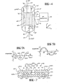
- FIG. 4 depicts one embodiment of an RF coil useful in performing NMR studies.
- the coil is claimed and disclosed in greater detail in the afore-identified patent application.
- the coil is made up of two conductive loop elements 60 and 62 spaced apart along a common longitudinal axis 64.
- the conductive loop elements are electrically interconnected by a plurality of conductors (smh as the one designated 66) each having a reactive element 68, preferably a capacitor, connected in series therewith.
- the coil embodiment depicted in FIG. 4 is shown as having eight conductors. In practice, the number of conductors may be varied and embodiments having as many as thirty-two such conductors have been fabricated.
- the conductors are separated along the peripheries of loop elements 60 and 62 by an angle E measured from, for example, the X axis.
- the preferred embodiment of the coil is constructed using flexible printed circuit board materials which are etched to provide the needed conductive paths.
- double-sided printed circuit boards may be utilized.
- Capacitors 68 are formed in a manner similar to that previously described with reference to FIG. 2 by etching gaps in a conductor 68 on one side of the printed circuit board such that the etched portion is overlapped by a continuous conductive portion on the other side of the printed circuit.
- the coil is energized by means of an RF amplifier 70 shown in block diagram form across a capacitor 68 by means of coil input leads 72 and 74.
- the current distribution in conductor 68 is generally sinusoidal and dependent on the angular position 8 of the conductor along the loop periphery.
- the current distribution in the coil is indicated in FIG. 4 by means of arrows 76. It will be noted that two diametrically opposed conductors 78 and 80 carry substantially no current.
- FIGS. 5A and SB depict graphically the current distribution in conductors 66 and in conductive loop elements 60 and 62, respectively.
- FIG. 6 depicts the etched pattern to be used on the two conductive surfaces separated by the dielectric material.
- Solid lines 82 designate the areas to be etched on the inner conducting sheet, (i.e., the conducting sheet which will form the inner cylindrical surface), while dotted lines 84 designate the areas to be etched in the outer conducting sheet.
- the etched printed circuit board can be formed into a cylinder suitable for positioning within the magnet bore by soldering edges A-B and C-D of the inner conducting sheet. As before, the edges of the outer conductive sheet are not electrically connected and form a gap as suggested by dashed lines 135 connecting points A-B and C-D.
- the inner and outer conductive sheets in a central rectangular region defined by letters E, F, G, and H of the decoupling shield are etched to create a plurality of vertical strips 88 and 86, respectively, which parallel the straight conductor element 66 (FIG. 4) on the cylindrical surface of the RF coil.
- the etched lines on each of inner and outer conducting surfaces are displaced relative to one another by one half of the strip width, for example, such that a gap on one conductive sheet is bridged by the co-extensively situated conductive strip on the other conductive sheet.
- Conductive strips 90, 91, and 92 on the inner conductive sheet and conductive strips 94, 95, and 96 conduct currents corresponding to those flowing in the conductive loop elements 60 and 62 of the RF coil.
- Conductive loop element 60 is centered on strip 92, while conductive loop element 62 is centered on strip 94. There are no discontinuities in these paths because the etched areas located along lines J-K and L-M can be positioned at points along the loop peripheries where the loop currents are at a minimum. As described hereinbefore, such points occur at angular positions e - 0° and 180° (FIG. SB). Etched lines 130 and 131 do impede vertical current flow. These cuts are necessary, however, to prevent gradient-induced eddy currents. In this area of the coil, however, the coil current is spread out over a wide area so that current densities are lower across lines 130 and 131 than in strips 92 and 94.
- Etched lines 132, 133, and 134 on the outer conductive sheet are located far from the corresponding etched lines 130 and 131 on the inner conductive sheet to maximize the capacitive bridging across lines 130 and 131.
- Etched lines 135 and 136 form a gap in the completed shield and on the outer conductive sheet prevent gradient-induced eddy current loops in the outer conductive sheet without producing any adverse effects on shield efficacy. It should be noted that none of the etched lines in the inner conducting sheet cross those on the outer conducting sheet. However, it may be desirable to permit such cross-overs as, for example, by joining lines 130 and 131 to form a single continuous etched line between points N and P.
- all vertical conductive elements such as those designated 88 will offer substantially the same impedance to currents induced on the inner surface. Unbalanced or unequal impedances in the inner shield surface could induce perturbations in the RF coil current distribution which would reduce the homogeneity of the RF field.
- Leaks in the decoupling shield will occur if an etched line in the inner conducting sheet crosses an etched line on the outer conductive sheet. At the intersection of the etched lines, there will be a small area with no conductive material. Such leaks can be eliminated by adding a second dielectric sheet (not shown) and a third conductive region (not shown) overlaying the intersection of the etched lines.
- the third conductive region may be, for example, 4 x 4 inches and centered on the intersecton. It is possible to avoid crossing of the etched lines by judicious choice of the patterns of the two conductive sheets as depicted in FIGS. 3 and 6.
- the inventive decoupling shield fabricated to operate at 64 mHz corresponding to the proton resonant frequency in a 1.5 Tesla magnetic field, it was found that one-ounce copper material for each of the inner and outer conductor sheets is adequate to contain the RF currents. It has been found additionally that printed circuit boards utilizing Teflon resin as the dielectric material between the two conductive sheets are preferred to minimize the loading of the RF coil.
- FIG. 7 depicts a side view of an etched line 140 in an inner conductive sheet 142.
- the etched line is formed transverse to the direction of current flow in the inner conducting sheet designated by arrows 144a.
- the RF magnetic field produced by the RF coil directed perpendicular to and outward from the plane of the figure, is indicated by dotted circles 146.
- the current passes through a dielectric material designated 154 as a displacement current indicated by dashed arrows 156.
- the current bridges etched line 140 by flowing along a surface 158 of the outer conducted sheet 160 adjacent to the dielectric material.
- the current re-crosses the dielectric material as indicated by dashed arrows 162 and then flows on surface 150b of inner conductive sheet 142 toward edge line 140 and out to the surface 148b (as indicated by arrows 144b) of the inner conductive sheet as required by tangential magnetic field represented by the dotted circles 146.
- the capacitance between the inner and outer conductive sheets should be large. This requires that dielectric material 154 be thin and that the etched lines on the outer conductive sheet 160 should be spaced far from the cut (such as cut 140) in the inner conductive sheet so as to provide a maximum area of overlap on either side of the etched line.
- an RF shield for decoupling RF and gradient coils without significantly degrading the performance of either coil.
- the shield is substantially transparent to the hotnogeneous magnetic field and audio frequency magnetic field gradients.
- the shield acts as a low-pass filter for time-dependent gradient magnetic fields and as an electrical short-circuit for RF fields.
Abstract
Description
- This invention relates to nuclear magnetic resonance (NMR) apparatus. More specifically, the invention relates to decoupling shields particularly useful in an NMR apparatus for decoupling radio-frequency (RF) and gradient coils.
- In general, the NMR apparatus includes a main magnet typically configured as a solenoid having a bore formed therein for accepting the NMR sample to be studied. The magnet which is frequently of a resistive or superconductive design is used to produce a homogeneous polarizing magnetic field in a predetermined region within the bore. The magnetic field is needed to polarize the nuclei within the sample, so that the NMR phenomenon can be excited. Magnetic fields utilized in NMR imaging and particularly those needed for in-vivo spectroscopy must be highly homogeneous to, for example, in excess of one part in a million. To achieve such degree of homogeneity, auxiliary field-correcting coils referred to as shim coils are provided in the magnet bore to provide the necessary correction factors. Radio-frequency coils constructed on cylindrical forms are positioned within the magnet bore coaxially with the longitudinal bore axis. The RF coils are used to irradiate the sample studied to excite the nuclear spins. Upon cessation of the RF excitation, the excited nuclei radiate an NMR signal which is detected with the same coil used to excite the resonance or with a separate coil orthogonally oriented with respect to the excitation coil. Additionally, in an NMR imaging apparatus three sets of gradient coils are provided within the bore. The gradient coils when energized are capable of producing three orthogonal, substantially linear magnetic field gradients each oriented along one of the directions of a conventional Cartesian coordinate system. The gradients are utilized in a well-known manner to encode into NMR signal spatial information of the nuclear spin distribution within the sample region excited by the RF coils. This information can be used to reconstruct images displaying one or more NMR parameters.
- Bore space in NMR magnets utilizied in whole-body NMR imaging is limited due to the fact that sufficient clearance must be provided to accommodate the human torso. The RF, gradient, and/or magnet shim coils are therefore situated in close proximity to one another. In a typical configuration, the RF coils are placed coaxially within the gradient coils. There can be numerous interactions between various coils which can degrade the performance of the RF coils. The gradient coils or shim coils can cause losses to occur in the RF coils. These losses can lower the quality factor Q of the RF coil resulting in a lower signal-to-noise ratio in the image. Although the signal-to-noise ratio can be improved by signal averaging, this is not a desirable solution since the NMR data collection time is unacceptably increased. The numerous windings within the gradient coils are coupled together by stray capacitances which can give rise to a plurality of spurious resonances when the RF coils are energized. If one or more of these spurious resonances interacts with the RF coil, the desired RF frequency may be displaced and the desired resonance damped. These detrimental effects increase with the proximity of the RF coils to the gradient coils.
- The interaction between the RF and gradient coils can be reduced or eliminated by placing an RF opaque screen between the gradient and RF coil forms. The screen must be several RF skin-depths thick to decouple the coils effectively. Suitable screens have been fashioned from copper mesh screen or copper foil having a thickness of .004 inches with a fiber backing. Such screens have been found effective in destroying RF interaction between the RF and gradient coils. A drawback associated with such simple shields is that the high-frequency response of the gradient coils is degraded. The rise time of the switched gradient field is lengthened by the eddy current induced in the continuous conductive layer of the RF shield.
- It is, therefore, an object of the invention to provide an RF shield for effectively decoupling the RF and gradient coils without significantly degrading coil performance.
- It is another object of the invention to provide an RF shield which acts as a low-pass filter for the time-dependent magnetic fields produced by the gradient coils.
- It is a further object of the invention to provide an RF shield which is substantially transparent to homogeneous magnetic field and audio frequency gradient magnetic fields but which is highly reflective with low loss for RF magnetic fields.
- An NIR apparatus includes means for producing a homogeneous magnetic field, a radio-frequency (RF) coil for transmitting and receiving RF energy, and gradient coils for generating pulsed linear magnetic field gradients at audio frequencies. A decoupling shield disposed between the RF and gradient coils is made up of first and second arrays of electrically conductive regions separated by relatively narrow non-conductive regions. The arrays are disposed on opposite surfaces of a member formed of a high dielectric material, and are offset relative to one another such that the conductive regions of the one array bridge the non-conductive regions of the other array to form a plurality of capacitive elements. In operation, the capacitive elements act essentially as electrical short circuits at radio frequencies and transmit substantially unaffected the homogeneous magnetic field and audio frequencies associated with the pulsed magnetic field gradients.
- The features of the invention believed to be novel are set forth with particularity in the appended claims. The invention itself, however, both as to its organization and method of operation, together with further objects and advantages thereof, may best be understood by reference to the following description taken in conjunction with the accompanying drawings in which:
- FIGURE 1 is a cross-sectional view of an NMR magnet depicting RF, gradient, and shim coil assemblies, including an RF shield;
- FIGURES 2 and 3 depict exemplary embodiments of an RF shield in accordance with the invention;
- FIGURE 4 depicts schematically an RF coil particularly useful in NMR studies and with respect to which a preferred embodiment of the RF shield will be disclosed;
- FIGURES 5A and 5B depict graphically the current distributions in the coil shown in FIG. 4;
- FIGURE 6 depicts a preferred embodiment of the inventive RF shield useful with the RF coil depicted in FIG. 4; and
- FIGURE 7 depicts a sectional side view of a cut in the inner shield surface transverse to current flow with reference to which shield operation is described.
- FIGURE 1 depicts a side cross-sectional view of a superconductive KqR magnet generally designated 10. The magnet is of a solenoidal construction having a
cylindrical bore 12 centered about alongitudinal axis 14. The magnet is provided with a set ofmain coil windings 16 which when energized produced the polarizing magnetic field. In the superconductive magnet the main coils are disposed within acryostat 18 containing suitable cryogens, such as liquid helium and nitrogen for maintaining the coil windings at superconductive temperatures characteristic of the materials used in the coils. One or more sets ofshim coils 20 which may be of resistive or superconductive design are typically provided to correct for magnetic field inhomogeneities inherent in the main coil windings. Superconductive shim coils would, of course, be housed withincryostat 18. Shim coils of resistive or superconductive design are advantageously placed adjacent to the main coil windings. AnRF coil assembly 22 is positioned coaxially inside agradient coil assembly 24. AnRF decoupling shield 26 is positioned coaxially between the RF and gradient coil assemblies. A region of the patient (not shown) to be examined is aligned with a generallyspherical volume 28 where the polarizing and RF magnetic fields are homogeneous and where the gradient magnetic field produced by the gradient coil assemblies are linear. - One embodiment of a decoupling RF shield in accordance with the invention will now be described with reference to FIG. 2. The shield is made up of two
sheets thin layer 36 of a low-loss flexible dielectric material such as Teflon synthetic resin polymer or polyethelene thermo-plastic polymer. In the preferred embodiment of the invention, the shield is constructed utilizing a double-sided copper-clad Teflon resin printed circuit board. Each ofcopper layers orthogonal lines copper sheet 34 is offset with respect to the pattern (depicted by solid lines) onsheet 32 by one half the width ofrectangular areas 38. The size of eacharray element 38 is made sufficiently small to minimize the eddy current effects at audio frequencies induced by the pulsed magnetic field gradients. At radio frequencies, the gaps formed by etchedlines dielectric material 36 is preferably selected to be very small, typically of the order of .004-.008 in.,-so as to create a large capacitance between the copper layers. In this manner, the gaps in conductivity on one copper sheet are capacitively shorted by conductors on the other side. At radio frequencies, the shield appears to be a single continuous conductor which is opaque to RF magnetic fields. The effect of the capacitive coupling is negligible at audio frequencies associated with the magnetic-field gradient pulses. An RF decoupling shield for use in an N41 apparatus is formed by shaping the flat printed circuit board into a cylindrical tube which is sized to fit against the gradient coil assembly. The cylinder is configured such thatsheet 32 comprises the inner cylindrical shield surface. To this end, edge A-A is joined to edge B-B ofsheet 32 to form electrically conductive joints between the half-size conductive areas (e.g., 44a to 44b, 46a to 46b, and 48b to 48b, etc.). In the completed shield, edges A-A and B-B ofsheet 34 remain unconnected to form a gap. - It will be recognized that, although the invention has been described with reference to FIG. 2 depicting a rectangular grid pattern, there are other patterns which can be fashioned to provide the capacitive elements. One example of such an alternative pattern to be utilized with the inventive RF shield is depicted in FIG. 3. The pattern is a modification of the pattern described with reference to FIG. 2. In this case, the inner conductive sheet (i.e., the sheet comprising the inner cylindrical shield surface) is subdivided into a plurality of conductive strips such as those designated 52 by etched
lines 54 depicted in FIG. 3 by the solid lines. A pattern is etched on the outer conductive sheet to formstrips 55 as indicated by dashedlines solid etch line 56 to avoid cross-over regions which can cause RF field leakage to occur. As before, the two conductive sheets are separated by a thin dielectric material and the patterns are offset relative to one another such that the etched areas on one are bridged by conductive areas on the other so as to form capacitive elements which act as short circuits to RF currents. This embodiment is particularly useful with an RF coil of solenoidal construction in which the coil turns (hence, current flow) would be parallel toetched lines Etched line 56 perpendicular toetched lines 54 prevents circumferential eddy currents (induced by pulsed magnetic field gradients) instrips 52 when the shield is formed into a cylinder. - The RF decoupling shield described hereinabove with reference to FIGS. 2 and 3 performs adequately. RF shields having improved performance, however, may be constructed if the current flow induced in the shield by the magnetic field generated by the RF coil is considered. The RF magnetic field is deflected by the currents induced in the shield surface closest to the RF coil (referred to as the inner shield surface). The currents induced in the shield are proportional and perpendicular to the tangential components of the RF magnetic field. When the RF coil is positioned near the RF shield as is the case in typical design, the current distribution in the inner shield surface essentially replicates the current in the coil elements. Etched (non-conductive) areas in the inner surface of the shield which run parallel to the direction of current flow in the coil elements will have minimal adverse effect on the performance of the shield. It is desirable, therefore, that the pattern of etched lines on the inner surface of the shield be tailored to match the particular RF coil geometry employed. Generally, it is necessary to etch areas so as to provide matching conductive strips on the inner shield surface which are parallel to and centered on each of the conductors in the RF coil structure. The manner in which this is accomplished will be described hereinafter with respect to a particular coil configuration disclosed and claimed in European application 841128846 filed in the name of the same inventor as herein and which is incorporated herein by reference.
- Some of the etched lines in the inner shield surface must be made perpendicular to the direction of the currents induced by the RF coil in order to eliminate large gradient-induced eddy current loops. The etched lines should be fabricated where the surface current density is smallest. Advantageously, the lines may be etched at places on the shield where surface current is zero or negligible due to the symmetry of the RF coil which results in some of the coil conductors not carrying any appreciable currents.
- Another embodiment of the invention will now be disclosed with reference to FIG. 4 which depicts one embodiment of an RF coil useful in performing NMR studies. The coil is claimed and disclosed in greater detail in the afore-identified patent application. Briefly, the coil is made up of two conductive loop elements 60 and 62 spaced apart along a common
longitudinal axis 64. The conductive loop elements are electrically interconnected by a plurality of conductors (smh as the one designated 66) each having areactive element 68, preferably a capacitor, connected in series therewith. The coil embodiment depicted in FIG. 4 is shown as having eight conductors. In practice, the number of conductors may be varied and embodiments having as many as thirty-two such conductors have been fabricated. The conductors are separated along the peripheries of loop elements 60 and 62 by an angle E measured from, for example, the X axis. The preferred embodiment of the coil is constructed using flexible printed circuit board materials which are etched to provide the needed conductive paths. Advantageously, double-sided printed circuit boards may be utilized.Capacitors 68 are formed in a manner similar to that previously described with reference to FIG. 2 by etching gaps in aconductor 68 on one side of the printed circuit board such that the etched portion is overlapped by a continuous conductive portion on the other side of the printed circuit. The coil is energized by means of anRF amplifier 70 shown in block diagram form across acapacitor 68 by means of coil input leads 72 and 74. In operation, the current distribution inconductor 68 is generally sinusoidal and dependent on the angular position 8 of the conductor along the loop periphery. The current distribution in the coil is indicated in FIG. 4 by means ofarrows 76. It will be noted that two diametricallyopposed conductors - Current distribution in the RF coil described with reference to FIG. 4 will now be discussed with reference to FIGS. 5A and SB which depict graphically the current distribution in
conductors 66 and in conductive loop elements 60 and 62, respectively. Referring first to FIG. SA, it will be noted that the current distribution inconductors 66 is substantially sinusoidal with maximum current magnitudes (indicated along the vertical axis) occurring at angles of e = 0 and 18CP as indicated along the horizontal axis. Current minima occur atconductors conductor 66 at which the coil is energized. In this case, it will seen that maximum currents occur at angles of 6= 90° and 270°, while current minima occur at an angles of 0° and 180°. - One embodiment of a decoupling shield useful with the RF coil described with reference to FIG. 4 is depicted in FIG. 6. FIGURE 6 depicts the etched pattern to be used on the two conductive surfaces separated by the dielectric material.
Solid lines 82 designate the areas to be etched on the inner conducting sheet, (i.e., the conducting sheet which will form the inner cylindrical surface), whiledotted lines 84 designate the areas to be etched in the outer conducting sheet. The etched printed circuit board can be formed into a cylinder suitable for positioning within the magnet bore by soldering edges A-B and C-D of the inner conducting sheet. As before, the edges of the outer conductive sheet are not electrically connected and form a gap as suggested by dashedlines 135 connecting points A-B and C-D. The inner and outer conductive sheets in a central rectangular region defined by letters E, F, G, and H of the decoupling shield are etched to create a plurality ofvertical strips Conductive strips conductive strips strip 94. There are no discontinuities in these paths because the etched areas located along lines J-K and L-M can be positioned at points along the loop peripheries where the loop currents are at a minimum. As described hereinbefore, such points occur at angular positions e - 0° and 180° (FIG. SB).Etched lines 130 and 131 do impede vertical current flow. These cuts are necessary, however, to prevent gradient-induced eddy currents. In this area of the coil, however, the coil current is spread out over a wide area so that current densities are lower acrosslines 130 and 131 than instrips 92 and 94. Additionally, larger areas of capacitivecoupling bridge lines 130 and 131.Etched lines lines 130 and 131 on the inner conductive sheet to maximize the capacitive bridging acrosslines 130 and 131.Etched lines lines 130 and 131 to form a single continuous etched line between points N and P. In this case, all vertical conductive elements such as those designated 88 will offer substantially the same impedance to currents induced on the inner surface. Unbalanced or unequal impedances in the inner shield surface could induce perturbations in the RF coil current distribution which would reduce the homogeneity of the RF field. - Leaks in the decoupling shield will occur if an etched line in the inner conducting sheet crosses an etched line on the outer conductive sheet. At the intersection of the etched lines, there will be a small area with no conductive material. Such leaks can be eliminated by adding a second dielectric sheet (not shown) and a third conductive region (not shown) overlaying the intersection of the etched lines. The third conductive region may be, for example, 4 x 4 inches and centered on the intersecton. It is possible to avoid crossing of the etched lines by judicious choice of the patterns of the two conductive sheets as depicted in FIGS. 3 and 6.
- In one embodiment of the inventive decoupling shield fabricated to operate at 64 mHz corresponding to the proton resonant frequency in a 1.5 Tesla magnetic field, it was found that one-ounce copper material for each of the inner and outer conductor sheets is adequate to contain the RF currents. It has been found additionally that printed circuit boards utilizing Teflon resin as the dielectric material between the two conductive sheets are preferred to minimize the loading of the RF coil.
- The manner in which current flows across the etched lines in the shield will now be described with reference to FIG. 7 which depicts a side view of an etched line 140 in an inner
conductive sheet 142. The etched line is formed transverse to the direction of current flow in the inner conducting sheet designated by arrows 144a. The RF magnetic field produced by the RF coil, directed perpendicular to and outward from the plane of the figure, is indicated by dotted circles 146. When the current on the inner surface 148a ofconductive sheet 142 reaches etched line 140, it is deflected to theopposite side 150a of the inner conductive sheet and flows away from the etched line as indicated byarrows 152 directed in an opposite direction of arrows 144a. The current passes through a dielectric material designated 154 as a displacement current indicated by dashedarrows 156. The current bridges etched line 140 by flowing along asurface 158 of the outer conductedsheet 160 adjacent to the dielectric material. The current re-crosses the dielectric material as indicated by dashedarrows 162 and then flows onsurface 150b of innerconductive sheet 142 toward edge line 140 and out to thesurface 148b (as indicated by arrows 144b) of the inner conductive sheet as required by tangential magnetic field represented by the dotted circles 146. To minimize the voltages developed across etched line 140, the capacitance between the inner and outer conductive sheets should be large. This requires thatdielectric material 154 be thin and that the etched lines on the outerconductive sheet 160 should be spaced far from the cut (such as cut 140) in the inner conductive sheet so as to provide a maximum area of overlap on either side of the etched line. - It will be appreciated from the foregoing that in accordance with the invention there is provided an RF shield for decoupling RF and gradient coils without significantly degrading the performance of either coil. The shield is substantially transparent to the hotnogeneous magnetic field and audio frequency magnetic field gradients. In operation, the shield acts as a low-pass filter for time-dependent gradient magnetic fields and as an electrical short-circuit for RF fields.
- While this invention has been described with reference to particular embodiments and examples, other modifications and variations will occur to those skilled in the art in view of the above teachings. Accordingly, it should be understood that within the scope of the appended claims the invention may be practiced otherwise than is specifically described.
Claims (7)
Applications Claiming Priority (2)
| Application Number | Priority Date | Filing Date | Title |
|---|---|---|---|
| US562121 | 1983-12-16 | ||
| US06/562,121 US4642569A (en) | 1983-12-16 | 1983-12-16 | Shield for decoupling RF and gradient coils in an NMR apparatus |
Publications (3)
| Publication Number | Publication Date |
|---|---|
| EP0151726A2 true EP0151726A2 (en) | 1985-08-21 |
| EP0151726A3 EP0151726A3 (en) | 1985-12-04 |
| EP0151726B1 EP0151726B1 (en) | 1988-08-17 |
Family
ID=24244882
Family Applications (1)
| Application Number | Title | Priority Date | Filing Date |
|---|---|---|---|
| EP84114885A Expired EP0151726B1 (en) | 1983-12-16 | 1984-12-06 | A shield for decoupling rf and gradient coils in an nmr apparatus |
Country Status (4)
| Country | Link |
|---|---|
| US (1) | US4642569A (en) |
| EP (1) | EP0151726B1 (en) |
| JP (1) | JPS60177249A (en) |
| DE (1) | DE3473527D1 (en) |
Cited By (16)
| Publication number | Priority date | Publication date | Assignee | Title |
|---|---|---|---|---|
| EP0216590A1 (en) * | 1985-09-20 | 1987-04-01 | Btg International Limited | Magnetic field screens |
| DE3807178A1 (en) * | 1987-03-06 | 1988-09-29 | Toshiba Kawasaki Kk | MAGNETIC RESONANCE IMAGE DEVICE |
| EP0293723A2 (en) * | 1987-06-04 | 1988-12-07 | Siemens Aktiengesellschaft | Magnetic coil system of an NMR imaging system, with superconducting coils and a shield for protection against eddy currents |
| EP0430104A2 (en) * | 1989-11-28 | 1991-06-05 | Kabushiki Kaisha Toshiba | Magnetic resonance imaging apparatus |
| EP0514140A1 (en) * | 1991-05-17 | 1992-11-19 | Koatsu Gas Kogyo Co., Ltd. | Superconductor magnetic shield |
| EP0532704A1 (en) * | 1990-06-06 | 1993-03-24 | Advanced Nmr Systems Inc. | Shielded gradient coil for nuclear magnetic resonance imaging |
| EP0580324A2 (en) * | 1992-07-24 | 1994-01-26 | Picker International, Inc. | Magnetic resonance apparatus |
| DE4225592A1 (en) * | 1992-08-03 | 1994-02-10 | Siemens Ag | Suppression of peripheral stimulations in NMR EPI tomography for preventing nerve stimulation or muscular spasm - providing closed conductor copper@ loop or mesh around stimulation-sensitive regions e.g. head, outside of region to be analysed |
| DE4232884A1 (en) * | 1992-09-30 | 1994-03-31 | Siemens Ag | Antenna arrangement for nuclear spin resonance device - has sub antennae with screens and flat conductor structures on pole plates |
| EP0644436A1 (en) * | 1993-09-21 | 1995-03-22 | Gec-Marconi Limited | Magnetic resonance apparatus |
| EP0724164A1 (en) * | 1995-01-27 | 1996-07-31 | Picker International, Inc. | Magnetic resonance apparatus and methods |
| US5574372A (en) * | 1994-01-19 | 1996-11-12 | Siemens Aktiengesellschaft | Diagnostic magnetic resonance apparatus having a radio frequency shield between the radio frequency antenna and the gradient coil system |
| US7098661B2 (en) * | 2003-10-01 | 2006-08-29 | Siemens Aktiengesellschaft | Magnetic resonance device with a high frequency shield having a high frequency short circuit to the circuits boundary surface of the basic field magnet |
| EP1895316A1 (en) * | 2006-09-01 | 2008-03-05 | Esaote S.p.A. | Removable electromagnetic shielding device for magnetic nuclear magnetic resonance apparati and method for making the same |
| US8013606B2 (en) | 2006-03-22 | 2011-09-06 | Koninklijke Philips Electronics N.V. | Shielded multix coil array for parallel high field MRI |
| CN109712773A (en) * | 2018-12-26 | 2019-05-03 | 中国科学院电工研究所 | A kind of high field nuclear magnetic resonance superconducting magnet |
Families Citing this family (76)
| Publication number | Priority date | Publication date | Assignee | Title |
|---|---|---|---|---|
| DE3347597A1 (en) * | 1983-12-30 | 1985-07-18 | Philips Patentverwaltung Gmbh, 2000 Hamburg | HIGH-FREQUENCY COIL ARRANGEMENT FOR GENERATING AND / OR RECEIVING ALTERNATIVE MAGNETIC FIELDS |
| JPS61290944A (en) * | 1985-06-18 | 1986-12-20 | 三洋電機株式会社 | Nuclear magnetic resonance tomographic apparatus |
| JPS62334A (en) * | 1985-06-26 | 1987-01-06 | 株式会社東芝 | Magnetic resonance imaging apparatus |
| JPS62117541A (en) * | 1985-11-18 | 1987-05-29 | 株式会社東芝 | Magnetic resonance imaging apparatus |
| DE3763625D1 (en) * | 1986-05-20 | 1990-08-16 | Siemens Ag | ANTENNA DEVICE FOR EXCITING AND / OR RECEIVING HIGH-FREQUENCY FIELDS IN A NUCLEAR SPIN TOMOGRAPHY APPARATUS. |
| JPH0652298B2 (en) * | 1986-08-13 | 1994-07-06 | 日本電子株式会社 | NMR coil |
| US4854040A (en) * | 1987-04-03 | 1989-08-08 | Poly Circuits, Inc. | Method of making multilayer pc board using polymer thick films |
| US4775573A (en) * | 1987-04-03 | 1988-10-04 | West-Tronics, Inc. | Multilayer PC board using polymer thick films |
| US4833392A (en) * | 1987-07-23 | 1989-05-23 | Regents Of The University Of California | Apparatus and method for measuring electrostatic polarization |
| US4820988A (en) * | 1987-10-07 | 1989-04-11 | The Regents Of The University Of California | Magnetic gradient coil set for nuclear magnetic resonace system having substantially different coil-patient spacings |
| US4833409A (en) * | 1987-12-21 | 1989-05-23 | General Electric Company | Apparatus for dynamically disabling an NMR field coil |
| US4820985A (en) * | 1988-04-06 | 1989-04-11 | General Electric Company | Apparatus for tuning an NMR field coil |
| JPH0722576B2 (en) * | 1988-04-11 | 1995-03-15 | 三菱電機株式会社 | Magnetic resonance device |
| NL8801162A (en) * | 1988-05-04 | 1989-12-01 | Philips Nv | SUPER CONDUCTIVE MAGNETIC SYSTEM WITH SUPER CONDUCTIVE CYLINDERS. |
| JPH022911A (en) * | 1988-06-17 | 1990-01-08 | Otsuka Denshi Kk | Method and apparatus for measuring nmr of organism tissue |
| USRE35064E (en) * | 1988-08-01 | 1995-10-17 | Circuit Components, Incorporated | Multilayer printed wiring board |
| US4871969A (en) * | 1988-12-22 | 1989-10-03 | General Electric Company | RF shield for RF coil contained within gradient coils of NMR imaging device |
| US4879515A (en) * | 1988-12-22 | 1989-11-07 | General Electric Company | Double-sided RF shield for RF coil contained within gradient coils of NMR imaging device |
| US5280248A (en) * | 1992-07-24 | 1994-01-18 | Picker International, Inc. | Biplanar RF coil for magnetic resonance imaging systems |
| US4980641A (en) * | 1989-08-11 | 1990-12-25 | General Atomics | Method and apparatus of reducing magnetic hysteresis in MRI systems |
| US5079069A (en) * | 1989-08-23 | 1992-01-07 | Zycon Corporation | Capacitor laminate for use in capacitive printed circuit boards and methods of manufacture |
| US5155655A (en) * | 1989-08-23 | 1992-10-13 | Zycon Corporation | Capacitor laminate for use in capacitive printed circuit boards and methods of manufacture |
| US5481191A (en) * | 1990-06-29 | 1996-01-02 | Advanced Nmr Systems, Inc. | Shielded gradient coil for nuclear magnetic resonance imaging |
| US5159929A (en) * | 1990-06-14 | 1992-11-03 | Morris G Ronald | Insulated rf shield |
| DE4030878A1 (en) * | 1990-09-29 | 1992-04-02 | Siemens Ag | DOUBLE SURFACE COIL FOR A NUCLEAR MIRROR |
| US5304932A (en) * | 1990-11-05 | 1994-04-19 | The Regents Of The University Of California | Apparatus and method for shielding MRI RF antennae from the effect of surrounding objects |
| JP3110115B2 (en) * | 1991-12-09 | 2000-11-20 | 株式会社東芝 | Magnetic resonance imaging equipment |
| US5218380A (en) * | 1992-02-21 | 1993-06-08 | Eastman Kodak Company | Platen drag mechanism for thermal printers |
| US5261153A (en) * | 1992-04-06 | 1993-11-16 | Zycon Corporation | In situ method for forming a capacitive PCB |
| US5800575A (en) * | 1992-04-06 | 1998-09-01 | Zycon Corporation | In situ method of forming a bypass capacitor element internally within a capacitive PCB |
| JP3233974B2 (en) * | 1992-04-09 | 2001-12-04 | 株式会社東芝 | High frequency magnetic field shield for MRI |
| AU4374993A (en) * | 1992-07-10 | 1994-01-31 | Doty Scientific, Inc. | Solenoidal, octopolar, transverse gradient coils |
| US5495171A (en) * | 1993-01-19 | 1996-02-27 | Fonar Corporation | Eddy current control in NMR imaging systems |
| US5432449A (en) * | 1993-02-25 | 1995-07-11 | General Electric Company | Test apparatus for magnetic resonance imaging systems |
| US5554929A (en) * | 1993-03-12 | 1996-09-10 | Doty Scientific, Inc. | Crescent gradient coils |
| US5530355A (en) * | 1993-05-13 | 1996-06-25 | Doty Scientific, Inc. | Solenoidal, octopolar, transverse gradient coils |
| US6728113B1 (en) * | 1993-06-24 | 2004-04-27 | Polychip, Inc. | Method and apparatus for non-conductively interconnecting integrated circuits |
| US5680046A (en) * | 1994-08-05 | 1997-10-21 | General Electric Company | Double-sided RF shield for RF coil contained within gradient coils used in high speed NMR imaging |
| DE4434951C2 (en) * | 1994-09-29 | 1996-08-22 | Siemens Ag | Magnetic resonance imaging device with a combination of high-frequency antenna and gradient coil |
| US5539314A (en) * | 1994-12-01 | 1996-07-23 | The Regents Of The University Of California | RF shield for four-post vertical field magnet used for MRI |
| US5572129A (en) * | 1995-01-19 | 1996-11-05 | The Regents Of The University Of California | RF shield for gradient coil |
| JPH08196518A (en) * | 1995-01-20 | 1996-08-06 | Toshiba Corp | Mri system |
| DE19742548C2 (en) * | 1997-09-26 | 1999-10-07 | Otten Ernst Wilhelm | Magnetic device for transport and storage of nuclear spin polarized gases and procedures for extracting these gases |
| KR100260509B1 (en) * | 1998-03-07 | 2000-07-01 | 이민화 | Active shielded high-order gradient coil for the head |
| US6157276A (en) * | 1998-08-14 | 2000-12-05 | General Electric Company | MRI magnet assembly with non-conductive inner wall |
| US6107974A (en) * | 1998-10-21 | 2000-08-22 | Fonar Corporation | Apparatus and method of generating an RF field |
| US6380735B1 (en) * | 1999-04-30 | 2002-04-30 | Sumitomo Special Metals Co., Ltd. | Orthogonal flux-gate type magnetic sensor |
| JP2003510111A (en) * | 1999-09-23 | 2003-03-18 | コーニンクレッカ フィリップス エレクトロニクス エヌ ヴィ | MRI apparatus including gradient coil with vacuum insulation |
| US6556012B2 (en) | 2000-01-21 | 2003-04-29 | Kabushiki Kaisha Toshiba | Magnetic resonance imaging apparatus |
| US6954068B1 (en) | 2000-01-21 | 2005-10-11 | Kabushiki Kaisha Toshiba | Magnetic resonance imaging apparatus |
| US6888153B2 (en) * | 2000-04-05 | 2005-05-03 | University Of Washington | Capacitive shield for containing radiofrequency magnetic fields |
| US6507190B1 (en) * | 2000-08-01 | 2003-01-14 | Ge Medical Systems Global Technologies Company Llc | Method and apparatus for compensating polarizing fields in magnetic resonance imaging |
| US20020073717A1 (en) * | 2000-12-19 | 2002-06-20 | Dean David E. | MR scanner including liquid cooled RF coil and method |
| US7504827B1 (en) | 2001-11-14 | 2009-03-17 | Fonar Corporation | MRI test fixture |
| DE10246310A1 (en) * | 2002-10-04 | 2004-04-22 | Siemens Ag | Gradient coil system for MRI machine is made up of two or more units fixed into tubular casing using adhesive |
| US7813145B2 (en) * | 2004-06-30 | 2010-10-12 | Endwave Corporation | Circuit structure with multifunction circuit cover |
| US20060002099A1 (en) * | 2004-06-30 | 2006-01-05 | Stoneham Edward B | Electromagnetic shield assembly |
| US7102350B2 (en) * | 2004-06-30 | 2006-09-05 | General Electric Company | Shielding apparatus for magnetic resonance imaging |
| US7425760B1 (en) | 2004-10-13 | 2008-09-16 | Sun Microsystems, Inc. | Multi-chip module structure with power delivery using flexible cables |
| CN101171526B (en) * | 2005-05-06 | 2012-07-18 | 皇家飞利浦电子股份有限公司 | Electromagnetic shielding for high field MRI coils |
| DE102005033989B4 (en) | 2005-07-21 | 2008-07-10 | Bruker Biospin Ag | Nuclear magnetic resonance apparatus with Gradientenabschirmanordnung with reduced coupling to the resonator system |
| US8233985B2 (en) * | 2005-11-04 | 2012-07-31 | Kenergy, Inc. | MRI compatible implanted electronic medical device with power and data communication capability |
| US8255054B2 (en) * | 2005-11-04 | 2012-08-28 | Kenergy, Inc. | MRI compatible implanted electronic medical device |
| US7295012B1 (en) * | 2006-04-28 | 2007-11-13 | General Electric Company | Methods and apparatus for MRI shim elements |
| CN101467060A (en) * | 2006-06-15 | 2009-06-24 | 皇家飞利浦电子股份有限公司 | Silent and thin RF body coil |
| US8836332B2 (en) | 2009-07-15 | 2014-09-16 | Viewray Incorporated | Method and apparatus for shielding a linear accelerator and a magnetic resonance imaging device from each other |
| US9013185B2 (en) * | 2011-03-07 | 2015-04-21 | Robert W. Brown | Optimized RF shield design |
| US8981779B2 (en) | 2011-12-13 | 2015-03-17 | Viewray Incorporated | Active resistive shimming fro MRI devices |
| DE102012212574B4 (en) * | 2012-07-18 | 2017-01-12 | Siemens Healthcare Gmbh | Method for electromagnetic shielding for a magnetic resonance system and correspondingly shielded device |
| US9446263B2 (en) | 2013-03-15 | 2016-09-20 | Viewray Technologies, Inc. | Systems and methods for linear accelerator radiotherapy with magnetic resonance imaging |
| JP6462292B2 (en) | 2014-09-26 | 2019-01-30 | キヤノンメディカルシステムズ株式会社 | Magnetic resonance imaging system |
| EP3559690B1 (en) * | 2016-12-22 | 2021-08-18 | Koninklijke Philips N.V. | Rf coil device and rf shield device for different mri modes |
| CN111712298B (en) | 2017-12-06 | 2023-04-04 | 优瑞技术公司 | Radiation therapy system |
| EP3617729A1 (en) | 2018-08-31 | 2020-03-04 | Skope Magnetic Resonance Technologies AG | Magnetic field probe for magnetic resonance imaging (mri) applications |
| WO2019243271A1 (en) | 2018-06-17 | 2019-12-26 | Skope Magnetic Resonance Technologies Ag | Magnetic field probe for magnetic resonance imaging (mri) applications |
| EP4302106A1 (en) * | 2021-03-04 | 2024-01-10 | Koninklijke Philips N.V. | Radio frequency coil with t-shaped connector between electrical conductors and radio frequency shield |
Citations (4)
| Publication number | Priority date | Publication date | Assignee | Title |
|---|---|---|---|---|
| DE1901793B2 (en) * | 1969-01-15 | 1972-06-22 | Licentia Patent Verwaltungs GmbH, 6000 Frankfurt | ARRANGEMENT FOR SHIELDING HIGH FREQUENCY PULSES IN MAINS FREQUENCY TRANSFORMERS |
| DE2942020A1 (en) * | 1978-10-17 | 1980-05-08 | Nat Res Dev | COIL FOR GENERATING MAGNETIC FIELDS OF SQUADRUPOLAR DESIGN |
| EP0067933A1 (en) * | 1981-06-13 | 1982-12-29 | Bruker Analytische Messtechnik GmbH | Electromagnet for NMR tomography |
| EP0073375A2 (en) * | 1981-08-24 | 1983-03-09 | Siemens Aktiengesellschaft | High-frequency device in a nuclear spin resonance apparatus |
Family Cites Families (5)
| Publication number | Priority date | Publication date | Assignee | Title |
|---|---|---|---|---|
| US3409805A (en) * | 1965-08-12 | 1968-11-05 | Foxboro Co | Printed-circuit board coupling circuit with d-c isolation |
| GB1190411A (en) * | 1967-03-30 | 1970-05-06 | English Electric Valve Co Ltd | Improvements in or relating to Television and Like Camera Tube Arrangements |
| US3569823A (en) * | 1968-10-18 | 1971-03-09 | Perkin Elmer Corp | Nuclear magnetic resonance apparatus |
| US4439733A (en) * | 1980-08-29 | 1984-03-27 | Technicare Corporation | Distributed phase RF coil |
| US4456881A (en) * | 1982-01-18 | 1984-06-26 | Technicare Corporation | Gradient-coil apparatus for a magnetic resonance system |
-
1983
- 1983-12-16 US US06/562,121 patent/US4642569A/en not_active Expired - Lifetime
-
1984
- 1984-12-06 EP EP84114885A patent/EP0151726B1/en not_active Expired
- 1984-12-06 DE DE8484114885T patent/DE3473527D1/en not_active Expired
- 1984-12-14 JP JP59263126A patent/JPS60177249A/en active Granted
Patent Citations (4)
| Publication number | Priority date | Publication date | Assignee | Title |
|---|---|---|---|---|
| DE1901793B2 (en) * | 1969-01-15 | 1972-06-22 | Licentia Patent Verwaltungs GmbH, 6000 Frankfurt | ARRANGEMENT FOR SHIELDING HIGH FREQUENCY PULSES IN MAINS FREQUENCY TRANSFORMERS |
| DE2942020A1 (en) * | 1978-10-17 | 1980-05-08 | Nat Res Dev | COIL FOR GENERATING MAGNETIC FIELDS OF SQUADRUPOLAR DESIGN |
| EP0067933A1 (en) * | 1981-06-13 | 1982-12-29 | Bruker Analytische Messtechnik GmbH | Electromagnet for NMR tomography |
| EP0073375A2 (en) * | 1981-08-24 | 1983-03-09 | Siemens Aktiengesellschaft | High-frequency device in a nuclear spin resonance apparatus |
Cited By (28)
| Publication number | Priority date | Publication date | Assignee | Title |
|---|---|---|---|---|
| EP0216590A1 (en) * | 1985-09-20 | 1987-04-01 | Btg International Limited | Magnetic field screens |
| JPS62143012A (en) * | 1985-09-20 | 1987-06-26 | ブリティッシュ・テクノロジー・グループ・リミテッド | Magnetic shield |
| DE3807178A1 (en) * | 1987-03-06 | 1988-09-29 | Toshiba Kawasaki Kk | MAGNETIC RESONANCE IMAGE DEVICE |
| US5028872A (en) * | 1987-03-06 | 1991-07-02 | Kabushiki Kaisha Toshiba | Magnetic resonance imaging system |
| EP0293723A2 (en) * | 1987-06-04 | 1988-12-07 | Siemens Aktiengesellschaft | Magnetic coil system of an NMR imaging system, with superconducting coils and a shield for protection against eddy currents |
| EP0293723A3 (en) * | 1987-06-04 | 1990-04-25 | Siemens Aktiengesellschaft | Magnetic coil system of an nmr imaging system, with superconducting coils and a shield for protection against eddy currents |
| EP0430104A2 (en) * | 1989-11-28 | 1991-06-05 | Kabushiki Kaisha Toshiba | Magnetic resonance imaging apparatus |
| EP0430104A3 (en) * | 1989-11-28 | 1991-10-30 | Kabushiki Kaisha Toshiba | Magnetic resonance imaging apparatus |
| EP0532704A1 (en) * | 1990-06-06 | 1993-03-24 | Advanced Nmr Systems Inc. | Shielded gradient coil for nuclear magnetic resonance imaging |
| EP0532704A4 (en) * | 1990-06-06 | 1993-09-08 | Advanced Nmr Systems, Inc. | Shielded gradient coil for nuclear magnetic resonance imaging |
| EP0514140A1 (en) * | 1991-05-17 | 1992-11-19 | Koatsu Gas Kogyo Co., Ltd. | Superconductor magnetic shield |
| EP0580324A3 (en) * | 1992-07-24 | 1994-07-20 | Picker Int Inc | Magnetic resonance apparatus |
| EP0580324A2 (en) * | 1992-07-24 | 1994-01-26 | Picker International, Inc. | Magnetic resonance apparatus |
| US5610521A (en) * | 1992-07-24 | 1997-03-11 | Picker International, Inc. | Gradient and RF coil system without RF shield |
| DE4225592A1 (en) * | 1992-08-03 | 1994-02-10 | Siemens Ag | Suppression of peripheral stimulations in NMR EPI tomography for preventing nerve stimulation or muscular spasm - providing closed conductor copper@ loop or mesh around stimulation-sensitive regions e.g. head, outside of region to be analysed |
| DE4225592C2 (en) * | 1992-08-03 | 2001-12-13 | Siemens Ag | Method for suppressing peripheral stimulations in a magnetic resonance imaging device |
| US5467017A (en) * | 1992-09-30 | 1995-11-14 | Siemens Aktiengesellschaft | Antenna arrangement for a nuclear magnetic resonance apparatus |
| DE4232884A1 (en) * | 1992-09-30 | 1994-03-31 | Siemens Ag | Antenna arrangement for nuclear spin resonance device - has sub antennae with screens and flat conductor structures on pole plates |
| US5577504A (en) * | 1993-09-21 | 1996-11-26 | Gec-Marconi Limited | Magnetic resonance apparatus |
| EP0644436A1 (en) * | 1993-09-21 | 1995-03-22 | Gec-Marconi Limited | Magnetic resonance apparatus |
| US5574372A (en) * | 1994-01-19 | 1996-11-12 | Siemens Aktiengesellschaft | Diagnostic magnetic resonance apparatus having a radio frequency shield between the radio frequency antenna and the gradient coil system |
| EP0724164A1 (en) * | 1995-01-27 | 1996-07-31 | Picker International, Inc. | Magnetic resonance apparatus and methods |
| US7098661B2 (en) * | 2003-10-01 | 2006-08-29 | Siemens Aktiengesellschaft | Magnetic resonance device with a high frequency shield having a high frequency short circuit to the circuits boundary surface of the basic field magnet |
| US8013606B2 (en) | 2006-03-22 | 2011-09-06 | Koninklijke Philips Electronics N.V. | Shielded multix coil array for parallel high field MRI |
| EP1895316A1 (en) * | 2006-09-01 | 2008-03-05 | Esaote S.p.A. | Removable electromagnetic shielding device for magnetic nuclear magnetic resonance apparati and method for making the same |
| US7772503B2 (en) | 2006-09-01 | 2010-08-10 | Esaote S.P.A. | Movable electromagnetic shielding device for nuclear magnetic resonance apparati and method for making the same |
| CN109712773A (en) * | 2018-12-26 | 2019-05-03 | 中国科学院电工研究所 | A kind of high field nuclear magnetic resonance superconducting magnet |
| CN109712773B (en) * | 2018-12-26 | 2021-10-01 | 中国科学院电工研究所 | Extremely high field nuclear magnetic resonance superconducting magnet |
Also Published As
| Publication number | Publication date |
|---|---|
| US4642569A (en) | 1987-02-10 |
| DE3473527D1 (en) | 1988-09-22 |
| EP0151726B1 (en) | 1988-08-17 |
| JPS60177249A (en) | 1985-09-11 |
| EP0151726A3 (en) | 1985-12-04 |
| JPH0350543B2 (en) | 1991-08-02 |
Similar Documents
| Publication | Publication Date | Title |
|---|---|---|
| EP0151726B1 (en) | A shield for decoupling rf and gradient coils in an nmr apparatus | |
| US6215307B1 (en) | Coils for magnetic resonance imaging | |
| US4692705A (en) | Radio frequency field coil for NMR | |
| US6437567B1 (en) | Radio frequency coil for open magnetic resonance imaging system | |
| US4439733A (en) | Distributed phase RF coil | |
| KR880001360B1 (en) | Radio frequency field coil for nmr | |
| US4680548A (en) | Radio frequency field coil for NMR | |
| US4799016A (en) | Dual frequency NMR surface coil | |
| EP0180121B1 (en) | Mutual inductance nmr rf coil matching device | |
| US5363845A (en) | Breast coil for magnetic resonance imaging | |
| EP2097763B1 (en) | Rf coil for use in an mr imaging system, in combination with a metamaterial | |
| US4686473A (en) | Device for creating and/or receiving an alternating magnetic field for an apparatus using nuclear magnetic resonance | |
| US4725779A (en) | NMR local coil with improved decoupling | |
| US5680046A (en) | Double-sided RF shield for RF coil contained within gradient coils used in high speed NMR imaging | |
| US20080129292A1 (en) | Rf Coil System for Super High Field (Shf) Mri | |
| KR930000895B1 (en) | Surface gradient assembly for high speed nuclear magnetic resonance imaging | |
| EP0177855B1 (en) | Radio frequency field coil for nmr | |
| GB2151791A (en) | RF Field coils for NMR apparatus | |
| Collins et al. | A method for accurate calculation ofb1fields in three dimensions. effects of shield geometry on field strength and homogeneity in the birdcage coil | |
| US8766636B2 (en) | MRI short coils | |
| US5663645A (en) | Spatially orthogonal rectangular coil pair suitable for vertical magnetic field MRI system | |
| US6175237B1 (en) | Center-fed paralleled coils for MRI | |
| US5381093A (en) | Magnetic resonance imaging apparatus | |
| CA2244847C (en) | Center-fed paralleled coils for mri | |
| JP3504968B2 (en) | Local coils for nuclear magnetic resonance imaging |
Legal Events
| Date | Code | Title | Description |
|---|---|---|---|
| PUAI | Public reference made under article 153(3) epc to a published international application that has entered the european phase |
Free format text: ORIGINAL CODE: 0009012 |
|
| AK | Designated contracting states |
Designated state(s): CH DE FR GB IT LI NL SE |
|
| PUAL | Search report despatched |
Free format text: ORIGINAL CODE: 0009013 |
|
| AK | Designated contracting states |
Designated state(s): CH DE FR GB IT LI NL SE |
|
| 17P | Request for examination filed |
Effective date: 19851126 |
|
| 17Q | First examination report despatched |
Effective date: 19860807 |
|
| GRAA | (expected) grant |
Free format text: ORIGINAL CODE: 0009210 |
|
| AK | Designated contracting states |
Kind code of ref document: B1 Designated state(s): CH DE FR GB IT LI NL SE |
|
| REF | Corresponds to: |
Ref document number: 3473527 Country of ref document: DE Date of ref document: 19880922 |
|
| ET | Fr: translation filed | ||
| ITF | It: translation for a ep patent filed |
Owner name: SAIC BREVETTI S.R.L. |
|
| PLBI | Opposition filed |
Free format text: ORIGINAL CODE: 0009260 |
|
| 26 | Opposition filed |
Opponent name: SIEMENS AKTIENGESELLSCHAFT, BERLIN UND MUENCHEN Effective date: 19890511 |
|
| NLR1 | Nl: opposition has been filed with the epo |
Opponent name: SIEMENS AG |
|
| PGFP | Annual fee paid to national office [announced via postgrant information from national office to epo] |
Ref country code: SE Payment date: 19901121 Year of fee payment: 7 |
|
| ITTA | It: last paid annual fee | ||
| PLBN | Opposition rejected |
Free format text: ORIGINAL CODE: 0009273 |
|
| STAA | Information on the status of an ep patent application or granted ep patent |
Free format text: STATUS: OPPOSITION REJECTED |
|
| 27O | Opposition rejected |
Effective date: 19901103 |
|
| NLR2 | Nl: decision of opposition | ||
| PG25 | Lapsed in a contracting state [announced via postgrant information from national office to epo] |
Ref country code: SE Effective date: 19911207 |
|
| REG | Reference to a national code |
Ref country code: GB Ref legal event code: 746 |
|
| PGFP | Annual fee paid to national office [announced via postgrant information from national office to epo] |
Ref country code: FR Payment date: 19921110 Year of fee payment: 9 |
|
| PGFP | Annual fee paid to national office [announced via postgrant information from national office to epo] |
Ref country code: CH Payment date: 19921117 Year of fee payment: 9 |
|
| PGFP | Annual fee paid to national office [announced via postgrant information from national office to epo] |
Ref country code: GB Payment date: 19921119 Year of fee payment: 9 |
|
| PGFP | Annual fee paid to national office [announced via postgrant information from national office to epo] |
Ref country code: NL Payment date: 19921231 Year of fee payment: 9 |
|
| REG | Reference to a national code |
Ref country code: FR Ref legal event code: DL |
|
| PG25 | Lapsed in a contracting state [announced via postgrant information from national office to epo] |
Ref country code: GB Effective date: 19931206 |
|
| PG25 | Lapsed in a contracting state [announced via postgrant information from national office to epo] |
Ref country code: LI Effective date: 19931231 Ref country code: CH Effective date: 19931231 |
|
| PG25 | Lapsed in a contracting state [announced via postgrant information from national office to epo] |
Ref country code: NL Effective date: 19940701 |
|
| GBPC | Gb: european patent ceased through non-payment of renewal fee |
Effective date: 19931206 |
|
| NLV4 | Nl: lapsed or anulled due to non-payment of the annual fee | ||
| PG25 | Lapsed in a contracting state [announced via postgrant information from national office to epo] |
Ref country code: FR Effective date: 19940831 |
|
| REG | Reference to a national code |
Ref country code: CH Ref legal event code: PL |
|
| REG | Reference to a national code |
Ref country code: FR Ref legal event code: ST |
|
| EUG | Se: european patent has lapsed |
Ref document number: 84114885.1 Effective date: 19920704 |
|
| PGFP | Annual fee paid to national office [announced via postgrant information from national office to epo] |
Ref country code: DE Payment date: 20021230 Year of fee payment: 19 |
|
| PG25 | Lapsed in a contracting state [announced via postgrant information from national office to epo] |
Ref country code: DE Free format text: LAPSE BECAUSE OF NON-PAYMENT OF DUE FEES Effective date: 20040701 |