EP0148477B1 - Exposure apparatus and method of aligning exposure mask with workpiece - Google Patents
Exposure apparatus and method of aligning exposure mask with workpiece Download PDFInfo
- Publication number
- EP0148477B1 EP0148477B1 EP84115889A EP84115889A EP0148477B1 EP 0148477 B1 EP0148477 B1 EP 0148477B1 EP 84115889 A EP84115889 A EP 84115889A EP 84115889 A EP84115889 A EP 84115889A EP 0148477 B1 EP0148477 B1 EP 0148477B1
- Authority
- EP
- European Patent Office
- Prior art keywords
- alignment mark
- alignment
- light
- workpiece
- area section
- Prior art date
- Legal status (The legal status is an assumption and is not a legal conclusion. Google has not performed a legal analysis and makes no representation as to the accuracy of the status listed.)
- Expired - Lifetime
Links
Images


Classifications
-
- H—ELECTRICITY
- H01—ELECTRIC ELEMENTS
- H01L—SEMICONDUCTOR DEVICES NOT COVERED BY CLASS H10
- H01L21/00—Processes or apparatus adapted for the manufacture or treatment of semiconductor or solid state devices or of parts thereof
- H01L21/02—Manufacture or treatment of semiconductor devices or of parts thereof
- H01L21/04—Manufacture or treatment of semiconductor devices or of parts thereof the devices having at least one potential-jump barrier or surface barrier, e.g. PN junction, depletion layer or carrier concentration layer
- H01L21/18—Manufacture or treatment of semiconductor devices or of parts thereof the devices having at least one potential-jump barrier or surface barrier, e.g. PN junction, depletion layer or carrier concentration layer the devices having semiconductor bodies comprising elements of Group IV of the Periodic System or AIIIBV compounds with or without impurities, e.g. doping materials
- H01L21/30—Treatment of semiconductor bodies using processes or apparatus not provided for in groups H01L21/20 - H01L21/26
-
- G—PHYSICS
- G03—PHOTOGRAPHY; CINEMATOGRAPHY; ANALOGOUS TECHNIQUES USING WAVES OTHER THAN OPTICAL WAVES; ELECTROGRAPHY; HOLOGRAPHY
- G03F—PHOTOMECHANICAL PRODUCTION OF TEXTURED OR PATTERNED SURFACES, e.g. FOR PRINTING, FOR PROCESSING OF SEMICONDUCTOR DEVICES; MATERIALS THEREFOR; ORIGINALS THEREFOR; APPARATUS SPECIALLY ADAPTED THEREFOR
- G03F9/00—Registration or positioning of originals, masks, frames, photographic sheets or textured or patterned surfaces, e.g. automatically
- G03F9/70—Registration or positioning of originals, masks, frames, photographic sheets or textured or patterned surfaces, e.g. automatically for microlithography
- G03F9/7049—Technique, e.g. interferometric
Definitions
- a circuit pattern of a semiconductor device has been being minituarized year by year and a requirement for a precision for alignment of the pattern has been becoming more and more severe.
- a wafer alignment method or a global alignment method has been used.
- positions at several points on a periphery of a wafer chip are measured by an alignment optical system and a laser distance measurement device and chip exposure positions are calculated on a presumption that other chips are accurately aligned and the wafer is exposed by a step and repeat method.
- an alignment detection time is short, an exposure time to an entire area of the wafer is short and a throughput is high.
- a high alignment precision is not attained and a specification required in a future alignment is hardly met. Accordingly, it is necessary in future to align chip by chip.
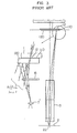
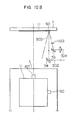
- FIG. 1 A prior art chip-by-chip alignment method is shown in Fig. 1.
- a circuit pattern of a mask or reticle 1 is to be exposed on a chip (or circuit pattern) 21 on a workpiece 2 such as a wafer
- a mirror 560' of alignment detection optical systems 500 and 560' for detecting the target marks must be penetrated into an exposure light flux 41.
- the mirror must be arranged outside of the exposure light flux as shown by 560.
- the wafer circuit pattern 21 and the target marks 22 and 22' may be arranged at positions corresponding to the circuit pattern 11 of the reticle and the target marks 12 and 12' of Fig. 1 as shown in Fig. 2 so that the alignment is attained at the exposure position.
- a distance from the circuit pattern 21 and the wafer target mark 22' must be larger than a predetermined length (1 mm)
- a width W S of an area (scribe area) between adjacent circuit patterns (chips) increases and a yield of the chip decreases and dusts are generated in cutting the chips.
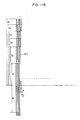
- Fig. 3 shows another prior art exposure position detection measure similar to that disclosed in U.S. Patent No. 4,357,100 issued on November 2, 1982.
- a protection glass 120 is mounted on a pattern surface 110 of a mask (reticle) 1, a light reflected by a target pattern 22 of a wafer 2 and transmitted through a reduction lens 3 is reflected by the protection glass 120 and further transmitted through a light splitting layer 16, and focussed, together with an optical image of the alignment target pattern 12, on a predetermined focusing plane through an enlarging/focusing lens 3', as shown more clearly in the left-hand portion of Fig. 3 representing an enlargement of the encircled part in the right-hand portion of Fig. 3.
- a protection glass is not protected from dusts and a pellicle layer (which is a high molecule layer having a thickness of several microns and which does not influence the imaging characteristic of the reduction lens) is placed on the reticle with a spacing of 6 to 10 mm therefrom.
- the protection glass has a thickness corresponding to such a spacing, the imaging characteristic of the reduction lens is influenced so that the resolution power is lowered.
- a device as shown in Fig. 4A is commercially available.
- an end of a detection system interrupts an exposure light from a circuit pattern A as shown in Fig. 4B, an image of a pattern is defocused if it is to be imaged in the vicinity of a wafer target. Accordingly, the pattern cannot be imaged in the vicinity of the target and only an area inside of a pattern B can be exposed as the circuit pattern.
- an exposure apparatus comprises
- a method of aligning an exposure mask plate with a workpiece having a workpiece alignment mark in an exposure apparatus in which the exposure mask plate includes an exposure pattern area section and an alignment area section and said exposure pattern area section is illuminated by first light source means to project images of patterns contained in an exposure pattern area section through projection lens means onto the workpiece being held on movable stage means comprises the steps of:
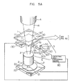
- an exposure apparatus includes an exposure light source 4, a reticle (mask plate means) 1, a projection lens, e.g., a reduction lens 3, a movable stage 7 for holding a photo-sensitive wafer (workpiece) 2 having alignment marks (wafer alignment marks) 22 and 22' and means (not shown) for driving the movable stage 7.
- the reticle 1 includes an exposure pattern area section including an area 11 and alignment/reflection reflection area section including areas 30 and 30' arranged adjacent thereto. Before the exposure pattern area 11 is illuminated by the light source 4 and an image thereof is projected on a chip 21 of a wafer 2 through the reduction lens 3, the alignment of the reticle 1 and the wafer 2 is carried out.
- the alignment/reflection areas 30 and 30' are arranged on that surface of the reticle 1 which does not face the light source 4 and each of the alignment/reflection areas 30 and 30' has a reflection portion and a mask alignment mark portion. Since the areas 30 and 30' are identical in construction and arrangement, only the area 30 is explained below.
- the reflection portion of the area 30 serves as a mirror when an alignment illumination light 501' is projected to the wafer alignment mark 22 adjacent to the chip 21 of the wafer 2 through a semitransparent mirror 55, an enlarging/focussing lens 52 and a mirror 51 and also serves to reflect scattered or reflected light transmitted through the reduction lens 3 from the wafer target mark 22' and direct it to an alignment detection unit 5 disposed out of an exposure light path.
- the reflection portion has a grating and a O-th order light (normal reflection light) is used to illuminate the wafer alignment mark 22 and detect its image.
- O-th order light normal reflection light
- elongated reticle target patterns Cr or Cr2O3 patterns or clear patterns
- the wafer alignment mark illumination light 501' is normally reflected by the reflection portion and directed to a center of the entrance pupil of the reduction lens 3.
- the incident light 501' to the wafer alignment mark 22 or 22' is scanned by a Galvanomirror 53 such that the illumination light falls within the entrance pupil circle.
- the scattered (reflection) light from the wafer alignment mark is focussed onto the alignment/reflection area 30, and after it is normally reflected, the image is refocused onto a detection element unit (imaging element unit) 50 so that a signal shown by a broken line in Fig. 5C is produced.
- the reticle alignment mask portion is illuminated by a reticle target illumination light 503 of another light path through the mirror 54.
- the incident angle of the illumination light to the alignment/reflection area 30 is different from that of the wafer illumination light and the direction of diffraction of the light primarily diffracted by the reflection portion corresponds to the direction of the light from the wafer alignment mark 22.
- a signal shown by a solid line in Fig. 5C is produced by the detection element unit 50.
- the light paths are sequentially switched so that the patterns are detected independently.
- the detected signals are fed to the detecting and processing means 80, in which centers of the waveforms of the detected signals are determined by known measures such as symmetrical pattern matching technique, information on the locations of the waveform centers are once stored in a memory at particular addresses and the positional deviation between the detected signals is determined from the address information.
- a control signal is then produced on the basis of the determined positional deviation and is used to drive the movable stage 7 or a reticle fine adjusting mechanism 130 so that a high precision alignment is attained.
- a control signal For the generation of the control signal, reference may be made to U.S. Patent 4153371 or U.S. Patent 4362389.
- Figs. 6A and 6B show another arrangement 30-1 of the alignment/reflection area section in the embodiment of the present invention in which the exposure light and the alignment light have substantially the same wavelength, and it is used as the area section 30 of the reticle shown in Fig. 5A.
- the reflection portion 30-1a is mostly coated with Cr or Cr2O3 except a reticle alignment pattern portion 30-1b which has a grating.
- the detection element unit 50 produces a signal as shown in Fig. 6B. In this case, the reticle alignment mark signal is high only for the grated target area.
- Figs. 7A and 7B show another arrangement 30-2 of the alignment/reflection area section in the embodiment of the present invention in which the exposure light and the alignment light have substantially the same wavelength.
- the reflection portion on the reticle has a uniform grating and left and right areas thereof are clear.
- the same detection unit as that of Fig. 5A may be used.
- a reticle signal and a wafer signal as shown in Fig. 7B are produced.
- Figs. 8A and 8B show another arrangement 30-3 of the alignment/reflection area section in the embodiment of the present invention in which the exposure light and the alignment light have substantially the same wavelength.
- a reflection portion 30-3a on the reticle is a uniform Cr or Cr2O3 surface.
- the reticle alignment mark detection illumination light 503 (and the mirror 54) shown in Fig. 5A should not be used and the wafer illumination light is also used to illuminate the reticle.
- An outline or contour 30-3b of the reflection portion 30-3a forms the reticle alignment mark portion, and a signal as shown in Fig. 8B is produced.
- the alignment mark signals of the wafer and the reticle are not simultaneously detected, unlike the embodiments shown in Figs. 5A, 6A and 7A.
- the wafer alignment mark illumination light is directed to the wafer alignment mark through the reduction lens.
- the light may be obliquely directed to the wafer alignment mark from the above of the wafer without passing through the reduction lens, provided that the scattered light from the wafer alignment mark is detected through the reduction lens.
- the alignment/reflection area section including a focusing pattern is arranged in adjacent to the exposure pattern area section as will be explained later, and the focusing pattern is illuminated by an essentially monochromatic light.
- the monochromatic light used need not be a physically pure monochromatic light but a light which can be practically considered as monochromatic may be sufficient for the present purpose.
- a wavelength of the monochromatic light is longer than the wavelength of the ordinary exposure light.
- the light reflected from the focusing pattern illuminated by the monochromatic light is diffracted and forms a condensed image.
- the condensed image is used as the mask alignment mark image.
- the image of the alignment mark on the chip of the wafer is focused in the vicinity of the mask alignment mark by the exposure or projection lens as will be explained later.
- the accurate alignment is attained.
- Fig. 9 shows a relation between image formation at the exposure wavelength of a focusing lens 3 of a semiconductor exposure apparatus and image formation at the alignment wavelength.
- a point P of a recticle 1 is sharply formed on the wafer by the exposure light (g-line) or dotted line light.
- the alignment lights 521 and 522 e-line
- the wafer alignment mark image is formed by the focusing lens 3 at a position P' which is displaced from the position P by ⁇ z.
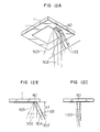
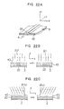
- An alignment/reflection area section including focusing patterns 60 and 60' is formed in a scribe area or bonding areas around an exposure pattern area section 11, in adjacent to the exposure pattern area section 11 on the mask 1.
- the focusing pattern may comprise hyperbolas as shown in Fig. 11A or quasi-hyperbolas as shown in Fig. 11B.
- the pattern comprises a number of hyperbolas or quasi-hyperbolas drawn by shifting a hyperbolar or quasi-hyperbola having a width w in a direction x (direction of a line connecting two focal points of the hyperbola) with a pitch p .
- a black or hatched area represents a Cr surface and a white area represents a Cr-free glass surface.
- the Cr surface forms the reflection portion.
- the width w and the lengths l1, l2, l3, ... of the hatched strips are determined such that they form a group of quasi-hyperbolas which will approximate a group of ideal hyperbolas as much as possible that can be drawn with an electron ray lithography apparatus.
- the alignment mark 22 in Fig. 10, in the scribe area on the wafer or the bonding area in the chip is obliquely illuminated by the e-lines 523 and 524 and the scattered light 503 is transmitted through the imaging lens 3 and the image is focused at the position P' in Fig. 9, directed to the alignment/reflection area section 60 along the light paths 503 and 503' of Fig. 12A, normally reflected (without diffraction) and focused at the position 1122.
- the focusing pattern is formed such that the area 60 and the focusing position 1122 are spaced by ⁇ z from each other.
- Fig. 12C is a view looked in a normal direction of the drawing in Fig.
- Fig. 13 shows the slit-shaped condensed image (Fig. 13C) by the diffraction light from the alignment/reflection area section formed in the vicinity of the position 1122 and the image (Fig. 13b) formed by obliquely illuminating the chip 21, transmitting the light therefrom through the focusing lens 3 and normally reflecting the light by the Cr surface of the alignment/reflection area section 60.
- the image from the chip 21 includes two peaks because of the scattered light created by the edges of the mark 22 (22'). Since a mid-point of the two peaks is a center of the mark 22 (22'), ⁇ x determined in a manner shown in Fig. 13d represents a positional deviation of the pattern.
- the deviation is focused onto the alignment detector 50 shown in Fig. 10A by the mirror 53 and the enlarging focusing lens 52 through the light path 504 shown in Figs. 10A and 10B so that an alignment control signal corresponding to the deviation is produced.
- the wafer 2 or the mask 1 is finely moved in accordance with the control signal so that the mask is perfectly aligned with the wafer. Generation of an alignment control signal and attainment of the alignment may be possible in the same manner as in Fig. 5A embodiment.
- the exposure light e.g. g-line
- the exposure light is emitted from the exposure light source means 4 so that the alignment and the exposure are carried out without a time lag and the total wafer exposure time is reduced.
- the alignment/reflection area section having the focusing pattern is arranged on that surface of the mask which does not face the exposure light source, in adjacent to the exposure pattern area section, the image of the reflected diffraction light created by illuminating the focusing pattern with the monochromatic light is detected as the reticle alignment mark image, the image of the alignment mark on the workpiece formed by the scattered light transmitted through the exposure or projection lens is detected and the alignment of those images is attained by driving the means for moving the mask or wafer.
- the mask (reticle) 1 has the exposure pattern area section including the area 11 and has the alignment/reflection area sections including areas 60 and 60' each carrying the focusing patterns, the alignment/reflection area sections being arranged on that surface of the mask 1 which does not face the exposure light source 4, at a position corresponding to the scribe area.
- the focusing pattern comprises hyperbolas or quasi-hyperbolas as shown in Fig. 11A or Fig. 11B.
- the hyperbolas are oriented such that they project toward the circuit pattern.
- the areas 60 and 61' may be rectangles having one side of 0.5 - 1 mm long and they are illuminated by a parallel beam of a He-Ne laser beam source 51 through a mirror 54 (Since the illumination and detection systems for the area 60' are identical to those for the area 60, they are not shown.)
- the He-Ne laser beam diffracted by the focusing pattern is condensed into a slit shape at the position 1122 shown in Fig. 10B.
- the chip 21 to be exposed is on the wafer on the movable wafer stage 7 and under the lens and at a position slightly deviated from the exact wafer position.
- the alignment mark on the scribe area of the wafer 2 is focused at 1122 by obliquely illuminating the alignment mark by the He-Ne laser beams 521 - 524 in four directions, transmitting the lights scattered by the edges of the alignment mark through the focusing lens 3 and normally reflecting the lights by the reflection portion of the area 60, that is, the Cr surface of the focusing pattern.
- the alignment mark image from the wafer formed at 1122 and the condensed image formed by the reflection and diffraction of the light from the mask are enlarged and focused on a detection plane (not shown) of the alignment detector 50 by the mirror 53 and the enlarging focusing lens 52 to determine the registration of both alignment mark images.
- the detection may be made by a solid-state imaging device or a combination of a scanning slit and a photo-multiplier. Misregistration of both patterns is detected and the control signal is generated.
- the wafer stage 7 or the mask 1 is moved in accordance with the control signal, and when the registration is attained, the exposure is carried out. Since the exposure light 41 is completely isolated from the alignment optical system and does not interfere, the exposure is completed immediately after the alignment.
- Figs. 14A and 14B show another embodiment of the present invention.
- the like elements to those shown in Figs. 10A and 10B are designated by the like numerals.
- the focusing patterns in the areas 60 and 60' of the alignment/reflection area sections adjacent to the exposure pattern area section including area 11 of the mask 1 are arranged at free locations in the bonding area in the exposure pattern area.
- the light from the e-line illumination light source 51'' of the mercury lamp is transmitted through the semitransparent mirror 56 along the light path 501, normally reflected by the reflection portion of the alignment/reflection area 60 including the focusing pattern such as that shown in Figs.
- the mask position may be determined by directing the monochromatic light 502 emitted from the He-Ne laser beam source, an Ar laser beam source or the e-line light source 51' to the alignment/reflection area 60 through the mirror 54 and detecting the slit-shaped image at 1122 by the diffraction light from the focusing pattern.
- the detection of the alignment mark images of the mask 1 and the wafer 2 and the alignment control are identical to those described in the above embodiment.
- Figs. 15A and 15B show another embodiment of the present invention.
- the like elements to those shown in Figs. 10A and 10B are designated by the like numerals.
- the light emitted from the semiconductor laser 51'' obliquely illuminates the alignment/reflection area 60 on the mask 1. Since the wavelength of the light is long, a primary diffraction angle is large and the primary diffracted light is returned in the incident direction and focused into a slit shape at position 1122.
- the light normally reflected by the reflection portion of the area 60 including the pattern as shown in Figs. 11A and 11B is transmitted along the light path 503' and used to illuminate the alignment mark in the scribe area of the wafer.
- the alignment mark of the wafer may be obliquely illuminated by the laser beams 521 - 524 in four directions, and the scattered light created by the step of the alignment mark of the wafer or the reflection light created by the illumination is normally reflected by the reflection portion of the area 60 and focused at 1122 as may be done in the previous embodiment.
- the detection of the signals of the alignment mark images of the mask and the wafer and the alignment control are now explained.
- Fig. 16 shows another arrangement of the alignment/reflection area section formed on the mask. It is particularly suitable for use in the exposure apparatus shown in Fig. 5A although it may be used in the exposure apparatus shown in other drawings.
- the alignment/reflection area section 61 has a reflection portion 61-1a at a center of the pattern and an alignment portions 61-1b including a focusing pattern at its side peripheries.
- the focusing pattern comprises a group of curves drawn by shifting a portion of a hyperbola in y-direction at a constant pitch, that is, a pattern of a group of hyperbolas.
- an electron beam lithography apparatus is usually used.
- the pattern is fine, it is difficult to smoothly draw a curved pattern. Accordingly, small rectangles having sides along the x-direction and y-direction may be arranged to simulate the hyperbola.
- the alignment/reflection area section 61 shown in Fig. 16 is arranged in the same manner as the alignment/reflection area 60 shown in Fig. 5A is arranged to align the wafer with the mask.
- the alignment light has a wavelength different from that of the exposure light, unlike in Fig. 5A embodiment.
- the wafer alignment mark is illuminated by directing the laser illumination light 501' through the galvanomirror 53, the beam splitter 55, the focusing lens 52 and the mirror or beam splitter 51 to the reflection portion 61-1a (Fig.
- the position of the image formed is determined by the wavelength of the laser beam 501' used for the alignment and a chromatic aberration of the reduction lens 3.
- the alignment/reflection area 61 has the center reflection portion 61-1a and the peripheral alignment mark portions 61-1b which contains the pattern of hyperbolas.
- the linear image 1122 is formed at the position of the image of the wafer alignment mark.
- a shape of the hyperbolas and a strength distribution of the linear image (change in the x-direction) for forming the linear image at the focusing positon of the wafer alignment mark (spaced from the lower surface of the reticle by h ) are now explained with reference to Figs. 17A - 17C.
- Fig. 17A shows the alignment/reflection area 61 on the reticle 1 and coordinates (x, y) exist on this plane.
- the mask alignment marks 61-1b which include the focusing patterns, that is, the hyperbola patterns (hyperbola gratings) are arranged on the opposite sides of the reflection portion 61-1a. Broken lines shown in the reflection portion 61-1a merely show connections of the left and right hyperbolas and they are not real patterns.
- Figs. 17B and 17C are side views of Fig. 17A, and x-y coordinates and y-z coordinates exist on the respective planes.
- the incident laser beam is a collimated beam which is in the y-z plane, makes an angle ⁇ 0 with the z-axis, is reflected and diffracted by the pattern of hyperbolas arranged at a pitch p to form the linear pattern 1122 at the position spaced from the lower surface of the reticle by h .
- the optical axis of the diffraction light makes an angle ⁇ 1 with the z-axis.
- the pattern of hyperbolas is represented by the following formula. where n is an integer. It is an aggregation of hyperbolas whose asymptotic curve is given by the following formula.
- the pitch p of the hyperbolas is given by This hyperbola grating (hyperbola pattern) does not exist in the reflection portion 61-1a as shown in Fig. 17A (broken lines) but exists in the alignment mark portions 61-1b on the opposite sides of the reflection area 61-1a.
- a width of the reflection portion 61-1a is represented by Wm and a total width of the hyperbola pattern (including the width of the reflection portion 61-1a) is represented by Wg.
- the width Wm should be at least a width of the illumination beam for the wafer alignment mark.
- the reflection portion 61-1a is too narrow and the illumination beam illuminates the hyperbola pattern, the reflected diffraction light therefrom is superimposed on the wafer alignment mark and an S/N ratio of a detection signal for the wafer alignment mark is reduced.
- the width is approximately equal to a product of a diameter of an illumination area necessary to detect the wafer alignment mark and a reciprocal of a reduction factor of the reduction lens.
- the reflected diffraction beam forms the linear image extending along the y-axis at the position spaced from the mask surface by h , as shown in Figs. 17B and 17C.
- An intensity distribution I(X) in the x-direction (coordinate on the linear image is X) is given by where C is a constant proportional to a laser beam intensity and a reflection factor. It is a pattern of a square of cosine waves having zero phase at a center of the pattern and having an envelope represented by I e 2 as shown by a broken line in Fig. 18.
- the center of the pattern can be precisely determined so that the position of the mask can be precisely determined.
- this pattern is formed on the same focusing plane ( h below the reticle surface) as that of the wafer alignment mark image formed by illuminating the wafer alignment mark by the laser beam and enlarging the image by the reduction lens (after the reflection by the reflection portion of the alignment/reflection area). Accordingly, as shown in Fig. 5A, it can be detected by the same detection system as that for the wafer alignment mark, by using the solid-state array device 50 through the mirror 51, focusing lens 52 and beam splitter 55.
- a drift of the detection position with time is zero as compared with a case where the marks are detected by two separate detection optical systems, and the optical system can be simplified and rendered inexpensive.
- the wafer target alignment mark and the diffraction image of the hyperbola pattern representing the reticle position are time-serially detected by the same detection system.
- the wafer 2 is moved by the array pitch of the chip by the x-y movable stage (wafer table) 7 so that an unexposed chip is brought under the reduction lens.
- the wafer alignment mark illumination laser beam 501' first illuminates the wafer alignment mark 22 so that the position thereof is detected by the solid-state array device 50.
- the laser beam 501' is extinguished and the illumination light 503 illuminates the alignment/reflection area (hyperbola pattern) on the reticle so that the reticle position is detected by the solid-state array device 50.
- a relative deviation is determined based on the two detected positons and it is compensated by finely adjusting the reticle 1 by the reticle (mask) fine adjusting mechanism 130. Since the distance of fine adjustment is the product of the reciprocal of the reduction factor of the reduction lens and the distance of the relative movement of the wafer 2, precise positioning is attained as compared to a case where the wafer 2 is moved. Since the positions of the wafer and the mask are time-serially detected, both detection patterns can be independently detected and the S/N ratio is not lowered by the other pattern. Thus, high precision detection is attained.
- the collimated laser beam is irradiated to the alignment/reflection area 61 at the incident angle ⁇ 0 when the reticle position is to be detected, but the light normally reflected by the area 61 is transmitted through the reduction lens 3 and illuminates the wafer alignment mark.
- the wafer alignment mark image may be superimposed on the diffraction linear image of the hyperbola pattern. This does not pose a substantial problem when the intensity of the diffraction linear image is high, but the influence of the superposition on the alignment precision cannot be neglected if the intensity of the reflection image of the wafer alignment mark is high or an extremely high alignment precision is required.
- the width W m of the reflection portion 61-1a of the area 61 shown in Figs. 17A to 17C is selected to a minimum required to illuminate the wafer alignment mark, and the width W g is selected to where NA is the number of aperture of the detection optical system. In this manner, W g -W m is selected to be large. As a result, a peak of the intensity of the hyperbola grating diffraction image (Fig. 18) is proportional to (W g -W m )2 and the reduction of the S/N ratio due to the superposition of the wafer pattern image is avoided.
- the recticle pattern of Fig. 16 does not use the conventional Cr mask but uses the Cr2O3 mask.
- the intensity I w of the wafer alignment mark image is proportional to r2 because the light is reflected twice in the illumination cycle and the imaging cycle.
- the intensity I m of the hyperbola pattern diffraction image representing the reticle position is proportional to r because the diffraction image is obtained by one reflection by the mask.
- a ratio of the intensity of the mask alignment mark diffraction image and the intensity of the wafer alignment mark image (noise image in detecting the mask alignment mark diffraction image), that is, the S/N ratio is given by Accordingly, the smaller the mask reflection factor is, the higher is the S/N ratio.
- the S/N ratio when the Cr2O3 mask is used is approximately four times as large as that when the Cr mask is used.
- Other low reflection factor materials than Cr2O3 may be used to attain the same effect. The effect will be satisfactory if the S/N ratio is at least three times as high as that obtained when the Cr mask is used.
- FIGs. 19A - 19C A third solution is shown in Figs. 19A - 19C. If the laser beam is irradiated only to the hyperbola pattern 61-1b on the opposite sides of the reflection portion 61-1a of the alignment/reflection area 61 and not irradiated to the wafer alignment mark 22, the wafer alignment mark image is not superimposed as the noise.
- a restrictive illumination mask 540 is inserted in the light path of the collimated illumination light beam 503 so that only the alignment mark portion 61-1b of the area 61 on the reticle 1.
- the mask 540 transmits the light in the area (openings) corresponding to the hyperbola pattern area and blocks the light in other areas.
- Fig. 19C illustrates how the area 61 in Fig. 19A is illuminated by the light 503 masked by the mask 540.
- the alignment portions 61-1b carrying hyperbolic patterns receive light 5401' representative of the images of the openings 5401.
- the focusing position of the wafer alignment mark image and the position of the diffraction image of the hyperbola pattern representing the reticle position are intentionally shifted from each other on the focusing plane.
- the amount of shift depends on the alignment precision in the step-and-repeat process of the wafer table and is to be larger than the line width of the wafer alignment mark.
- the mark or pattern is formed such that the wafer alignment mark and the diffraction image of the hyperbola pattern representing the reticle position are relatively shifted from each other by the above shift amount.
- the illumination light for the hyperbola pattern may be slightly shifted from the right angle by an angle made thereby with the x-axis as shown in Figs. 17A and 17C.
- the g-line, e-line and d-line which are spectrum lines of the mercury lamp or the He-Ne laser beam is used to align the patterns of the mask and the wafer.
- Such a light is irradiated through the exposure focusing lens. Since the exposure focusing lens is usually designed to exhibit a best focusing characteristic (high resolution power) only to the monochromatic light such as g-line, the spectrum width of the illumination light other than the exposure light must be narrow. However, for the light other than the exposure light, the focusing position on the optical axis varies significantly even for a slight change of the wavelength.
- the alignment detection pattern in order to attain the alignment detection pattern with a high resolution, it is necessary to use the light of as narrow spectrum width as possible.
- the light source other than the laser such as the mercury lamp cannot produce a light having a sufficiently narrow spectrum width and a sufficient intensity to allow the detection of the alignment mark on the wafer.
- the laser beam since the laser beam usually has a high coherence (spatial coherence), if the alignment mark on the wafer is marked by granular material such as Al or WSi, a noise called a speckle pattern is included in the mark image detection signal and the S/N ratio of the detection signal is lowered.
- a fine variation of the thickness of the resist layer may appear as a noise so that the S/N ratio of the detection signal is lowered.
- the alignment light has a wavelength different from that of the exposure light.
- Alignment/reflection area sections including areas 30 and 30' on the mask (reticle) 1 may contain the focusing patterns shown in Figs. 10A, 10B, 11A, 11B, 12A-12C and 13 and may be arranged on the mask 1 in the manner shown in those figures.
- Numeral 4 denotes an exposure light source.
- the light emitted from the laser beam source 90 is split by the beam splitter 91.
- One of the split beams illuminates the alignment/reflection area 30 containing the hyperbola pattern.
- the illumination light is diffracted and a primary diffraction light passes through a light path 601 and focused into a linear image at 600.
- the direction (x-direction) of the linear image represents the x-direction of the reticle 1.
- the other of the split beams is deflected by a Galvanomirror 92 which is an incident angle varying means.
- the deflected beam passes through a semitransparent mirror 83, a lens 84 and a mirror 85 and is directed to the alignment/reflection area 30 adjacent to the exposure pattern area 11 of the mask (reticle) 1, and the normally reflected light therefrom is directed into an entrance pupil 205 of the exposure focusing lens 3.
- the light 612 transmitted through the entrance pupil illuminates the alignment mark 22 (22') on the wafer arranged in the periphery of the chip 21 on the wafer 2.
- the chip 21 on the wafer 2 includes the elongated alignment marks 22 and 22' extending in the y-direction and the x-direction as shown in Fig.
- Figs. 20A and 20B only a control unit including an optical system for aligning the alignment mark 30 on the reticle 1 with the alignment mark 22 on the wafer 1 is shown as the alignment optical system, and another control unit including an optical system for aligning the mark 30' with the mark 22' is omitted because it may be identical.
- the laser beam directed to the alignment mark 22 on the wafer 1 in Figs. 20A and 20B has no change of incident angle in the x-z plane (x-direction) normal to the lengthwise direction of the alignment mark as shown in Fig. 22B, but the incident angle changes in the y-z plane (y-direction) normal to the mask 1 or the wafer 2 as shown in Fig. 22C.
- Fig. 22B shows a view of the alignment mark 22 on the wafer 2 (underlying layer of the alignment mark) as viewed in a direction A shown in Fig. 22A
- Fig. 22C is a view as viewed in a direction B.
- Numeral 43 in Figs. 22B and 22C denotes a resist film coated on the wafer 2.
- the light including the position information of the alignment mark 22 reflected by the wafer 2 is usually a diffraction pattern spreading in a direction (x-direction) normal to the lengthwise direction (y-direction) of the alignment mark on the wafer 1, as shown by 220, 221 and 222 in Fig. 23A, on the entrance pupil 205 of the exposure focusing lens 3 (x-y plane parallel to the mask 1 or the wafer 2). Accordingly, by deflecting the incident angle to the y-direction (normal to the x-axis) in the y-z plane as shown in Fig.
- the diffraction light information particularly the position information of the pattern to be detected (x-coordinate for the alignment mark 22 and y-coordinate for the mark 22') can be detected without loss.
- Fig. 23B shows the light deflected in the normal direction (x-direction in the z-x plane). In this case, the information in the direction to be detected is lost. The incident light is deflected in the direction shown in Figs.
- reticle alignment mark image The reticle alignment mark image and the wafer alignment mark image are transmitted through the mirror 85, lens 84 and beam splitter 83 and refocused on the imaging plane of the imaging means 81 by the focusing optical system 82.
- the wafer alignment mark image 22 and the mask alignment mark image 30 focused on the imaging plane of the imaging means 81 are shown in Fig. 25, in which numeral 600 denotes the imaging plane, numeral 30 denotes the image of the reticle window 30, and numeral 22 denotes the image of the alignment mark 22 of the wafer 2.
- a light intensity I t (i, j) is detected at time t for an address (i, j) of the array pixels.
- the detection signals in the longitudinal direction of the alignment mark 22 are summed. so that the signals are averaged and the S/N ratio is improved.
- the S/N ratio of the detection signal is still low even after the averaging as shown in Figs. 26A and 26B, in which the incident angles of the illumination light are fixed at different angles.
- the incident angle ⁇ is changed from time to time in the plane described above.
- the detection signal in the i-direction O ⁇ (i) is now represented by the following expression: Since the accumulation is usually done in the conventional imaging means, no special means is required.
- Figs. 27A - 27C show other modes of changing the incident angle to the wafer alignment mark.
- the incident angle is set by a step function
- Figs. 27B and 27C the incident angles are fixed depending on the alignment marks.
- Figs. 28A and 28B illustrate the illumination of the alignment mark in the multiple interference environment.
- ⁇ 514 nm
- the signal intensity changes as shown in Figs. 30A, 30B and 30C (which show the intensities detected in the x-direction when the resist layer thickness changes only depending on the shape of the underlying layer and is symmetric, or changes in accordance with the edge of the pattern).
- the signal ⁇ O is superimposed as the noise on the signals of Figs. 30A - 30C so that misdetection of the edge may occur when ⁇ O is large.
- I R denotes the reticle alignment mark image
- I W denotes the wafer alignment mark image.
- a deviation between the centers of those signal waveforms is detected by the detection system 80 and the wafer table 7 is moved in the x-direction (and also in the y-direction) to compensate for such deviation.
- shutters 62 and 63 are inserted in the respective light paths to detect the lights separately so that the centers of the signals I R and I W can be detected without error.
- Generation of the alignment control signal and alignment may be attained in the same manner as described with reference to Fig. 5A embodiment.
- a two-dimensional imager means such as a solid-state camera to detect images of wafer alignment marks and reticle alignment marks.
- these images carry only one-dimensional information, detection of these images is possible at a high speed and with a high resolution by the provision of a cylindrical lens before the imager means for compressing the lengthwise information of the images of the elongated or slender alignment marks and by the use of a one-dimensional array of imaging elements (e.g. CCD) for the imager means.
- the cylindrical lens and one-dimensional array may be, e.g., those disclosed in printed Japanese publications, Japanese Patent Publication No. 29045/83 or 53217/81.
- the alignment mark on the wafer is illuminated by the laser beam having the narrow spectrum width so that the defocusing due to the chromatic aberration of the exposure focusing lens is minimized and the level of the detection signal is kept sufficiently high.
- the incident angle of the laser beam can be controlled to an optimum angle in accordance with the semiconductor process such as the material of the resist layer, the thickness thereof, the shape of the underlying layer and the material thereof so that the noise due to the coherence of the laser beam is substantially reduced. Accordingly, the stability of the detection of the alignment pattern is significantly improved.
Landscapes
- Physics & Mathematics (AREA)
- General Physics & Mathematics (AREA)
- Engineering & Computer Science (AREA)
- Condensed Matter Physics & Semiconductors (AREA)
- Manufacturing & Machinery (AREA)
- Computer Hardware Design (AREA)
- Microelectronics & Electronic Packaging (AREA)
- Power Engineering (AREA)
- Exposure And Positioning Against Photoresist Photosensitive Materials (AREA)
- Exposure Of Semiconductors, Excluding Electron Or Ion Beam Exposure (AREA)
Description
- A circuit pattern of a semiconductor device has been being minituarized year by year and a requirement for a precision for alignment of the pattern has been becoming more and more severe. When the alignment precision is 0.3 µm or larger, a wafer alignment method or a global alignment method has been used. In this method, positions at several points on a periphery of a wafer chip are measured by an alignment optical system and a laser distance measurement device and chip exposure positions are calculated on a presumption that other chips are accurately aligned and the wafer is exposed by a step and repeat method. In this method, since only several positions on the chip need be measured, an alignment detection time is short, an exposure time to an entire area of the wafer is short and a throughput is high. However, in this method, because of the presumption of the alignment of the chips, a high alignment precision is not attained and a specification required in a future alignment is hardly met. Accordingly, it is necessary in future to align chip by chip.
- A prior art chip-by-chip alignment method is shown in Fig. 1. When a circuit pattern of a mask or
reticle 1 is to be exposed on a chip (or circuit pattern) 21 on aworkpiece 2 such as a wafer, ifalignment target marks circuit pattern 21 on the wafer, a mirror 560' of alignment detectionoptical systems 500 and 560' for detecting the target marks must be penetrated into anexposure light flux 41. In order to avoid this, the mirror must be arranged outside of the exposure light flux as shown by 560. In this arrangement, since images of thewafer target marks reduction lens 3 do not fall into a view field of the alignment detection optical system, thewafer 2 is to be sequentially moved to positions 21' and 21''. A distance of movement is measured by a laser distance measurement device, the target position is measured by the alignment detection optical system, an alignment position of the reticle and the wafer circuit pattern is calculated based on those measurements and the wafer is moved to that position and exposure is effected at that position. Such an extra wafer movement step leads to reduce the alignment precision and the throughput.Numerals 12 and 12' denote alignment target marks on the reticle. In order to avoid such an extra step, thewafer circuit pattern 21 and thetarget marks 22 and 22' may be arranged at positions corresponding to thecircuit pattern 11 of the reticle and thetarget marks 12 and 12' of Fig. 1 as shown in Fig. 2 so that the alignment is attained at the exposure position. In this method, however, since a distance from thecircuit pattern 21 and the wafer target mark 22' must be larger than a predetermined length (1 mm), a width WS of an area (scribe area) between adjacent circuit patterns (chips) increases and a yield of the chip decreases and dusts are generated in cutting the chips. - Fig. 3 shows another prior art exposure position detection measure similar to that disclosed in U.S. Patent No. 4,357,100 issued on November 2, 1982. A
protection glass 120 is mounted on apattern surface 110 of a mask (reticle) 1, a light reflected by atarget pattern 22 of awafer 2 and transmitted through areduction lens 3 is reflected by theprotection glass 120 and further transmitted through alight splitting layer 16, and focussed, together with an optical image of thealignment target pattern 12, on a predetermined focusing plane through an enlarging/focusing lens 3', as shown more clearly in the left-hand portion of Fig. 3 representing an enlargement of the encircled part in the right-hand portion of Fig. 3. In this prior art method, wavelengths of the exposure light and the alignment light are different from each other and an axial chromatic aberration due to the wavelength difference is compensated by fold-back of light by the protection glass and the light splitting layer. By this arrangement, alignment at the exposure position is attained. However, this method involves the following problems. (1) Since the axial chromatic aberration Δℓ (Δℓ = 3 - 10 mm) is not large enough to facilitate mounting of the optical system, a spacing between the protection glass and the light splitting layer is approximately Δℓ/2 which makes the mounting of the detection optical system difficult. (2) In this method, the light from the wafer target mark is reflected by the protection glass mounted on the lower surface of the reticle. However, such a protection glass is not protected from dusts and a pellicle layer (which is a high molecule layer having a thickness of several microns and which does not influence the imaging characteristic of the reduction lens) is placed on the reticle with a spacing of 6 to 10 mm therefrom. The larger the spacing from the reticle surface is, the less is the influence by the dusts. However, if the protection glass has a thickness corresponding to such a spacing, the imaging characteristic of the reduction lens is influenced so that the resolution power is lowered. - On the other hand, a device as shown in Fig. 4A is commercially available. In this device, however, since an end of a detection system interrupts an exposure light from a circuit pattern A as shown in Fig. 4B, an image of a pattern is defocused if it is to be imaged in the vicinity of a wafer target. Accordingly, the pattern cannot be imaged in the vicinity of the target and only an area inside of a pattern B can be exposed as the circuit pattern.
- It is an object of the present invention to provide a high throughput exposure apparatus also having a high alignment precision.
- It is another object of the present invention to provide a method of aligning an exposure mask with a workpiece in an exposure apparatus having a high precision.
- In accordance with one aspect of the present invention an exposure apparatus comprises
- first light source means,
- mask plate means having an exposure pattern area section and an alignment area section adjacent to said exposure pattern area section and including a mask alignment mark portion and being arranged so that said exposure pattern area section is illuminated by said first light source means,
- movable stage means for thereon holding a workpiece having a workpiece alignment mark,
- projection lens means interposed between said mask plate means and said movable stage means and disposed across said mask plate means from said first light source means so that said exposure pattern area section, when illuminated, is projected onto said workpiece through said projection lens means,
- alignment means for detecting the positional relation between said mask alignment mark portion of said alignment area section in said mask plate means and said workpiece alignment mark of said workpiece on said movable stage means and for producing a control signal for achieving alignment of said mask alignment mark portion with said workpiece alignment mark and
- driving means destined for adjusting the relative position between said mask plate means and said workpiece and adapted to be responsive to said control signal
- In accordance with another aspect of the present invention a method of aligning an exposure mask plate with a workpiece having a workpiece alignment mark in an exposure apparatus in which the exposure mask plate includes an exposure pattern area section and an alignment area section and said exposure pattern area section is illuminated by first light source means to project images of patterns contained in an exposure pattern area section through projection lens means onto the workpiece being held on movable stage means comprises the steps of:
- illuminating said alignment area section of said mask plate and said workpiece alignment mark
- detecting the positional relation between said alignment mark portion and said workpiece alignment mark
- producing a control signal representative of misregistration between said alignment mark portion and said workpiece alignment mark derived from the detected positional relation
and - adjusting the relative position between said exposure mask plate and said workpiece in accordance with said control signal,
- In the accompanying drawings:
- Figs. 1 to 3, 4A and 4B show prior art exposure apparatus and alignment methods;
- Figs. 5A to 5C show an exposure apparatus and an alignment method in accordance with one embodiment of the present invention in which exposure light and an alignment light have substantially the same wavelength;
- Figs. 6A, 6B, 7A, 7B, 8A and 8B show arrangements of an alignment/reflection area sections which may be used in the apparatus of Fig. 5 and signal waveforms representing a mask alignment mark image and a wafer alignment mark image;
- Fig. 9 shows images foussed by a projection lens for the exposure light and the alignment light having a different wavelength from that of the exposure light;
- Figs. 10A and 10B show an exposure apparatus and an alignment method in accordance with another embodiment of the present invention in which the exposure light and the alignment light have different wavelengths;
- Figs. 11A and 11B show an arrangement of the alignment/reflection area sections which may be used in the apparatus of Fig. 10A;
- Figs. 12A to 12C and 13 illustrate alignment in the apparatus of Fig. 10A;
- Figs. 14A, 14B, 15A and 15B show exposure apparatuses and an alignment methods in accordance with other embodiments of the present invention;
- Fig. 16 shows an arrangement of the alignment/reflection area section for the apparatus of Fig. 5A when the alignment light having a different wavelength from the exposure light is used;
- Figs. 17A to 17C and 18 illustrate an operation of the apparatus of Fig. 5A when the alignment/reflection area section of Fig. 16 is used;
- Figs. 19A to 19C show an improvement of the alignment/reflection area section of Fig. 16;
- Figs. 20A, 20B and 21 show exposure apparatuses and alignment methods in accordance with other embodiments of the present invention in which the exposure light and the alignment light have different wavelengths;
- Figs. 22A to 22C, 23A and 23B show an incident angle of the alignment light to a wafer alignment mark and an incident light to a projection lens from the wafer alignment mark;
- Fig. 24 shows a mode of change of the incident angle of the alignment light to the wafer alignment mark;
- Figs. 25 and 26A to 26C illustrate detection of alignment mark images in the apparatus of Figs. 20A and 20B;
- Figs. 27A to 27C show another mode of change of the incident angle of the alignment light to the wafer alignment mark;
- Figs. 28A and 28B illustrate multiple interference of alignment light caused by lamination of the wafer, alignment mark and resist layer;
- Fig. 29 shows a relation between a resist layer thickness and the multiple interference, with the incident angle of the alignment light being a parameter;
- Figs. 30A to 30C show signal waveforms when the alignment mark is detected in an ideal manner;
- Fig. 31 shows waveforms of detection signals for the alignment mark image in the apparatus of Fig. 20A.
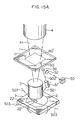
- Referring to Figs. 5A to 5C which show one embodiment in which the alignment is achieved by using an exposure light and an alignment light of the same wavelength, an exposure apparatus includes an exposure
light source 4, a reticle (mask plate means) 1, a projection lens, e.g., areduction lens 3, amovable stage 7 for holding a photo-sensitive wafer (workpiece) 2 having alignment marks (wafer alignment marks) 22 and 22' and means (not shown) for driving themovable stage 7. Thereticle 1 includes an exposure pattern area section including anarea 11 and alignment/reflection reflection areasection including areas 30 and 30' arranged adjacent thereto. Before theexposure pattern area 11 is illuminated by thelight source 4 and an image thereof is projected on achip 21 of awafer 2 through thereduction lens 3, the alignment of thereticle 1 and thewafer 2 is carried out. - The alignment/
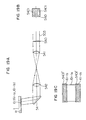
reflection areas 30 and 30' are arranged on that surface of thereticle 1 which does not face thelight source 4 and each of the alignment/reflection areas 30 and 30' has a reflection portion and a mask alignment mark portion. Since theareas 30 and 30' are identical in construction and arrangement, only thearea 30 is explained below. The reflection portion of thearea 30 serves as a mirror when an alignment illumination light 501' is projected to thewafer alignment mark 22 adjacent to thechip 21 of thewafer 2 through asemitransparent mirror 55, an enlarging/focussinglens 52 and amirror 51 and also serves to reflect scattered or reflected light transmitted through thereduction lens 3 from the wafer target mark 22' and direct it to an alignment detection unit 5 disposed out of an exposure light path. The reflection portion has a grating and a O-th order light (normal reflection light) is used to illuminate thewafer alignment mark 22 and detect its image. As shown in Fig. 5B, elongated reticle target patterns (Cr or Cr₂O₃ patterns or clear patterns) are recorded on thearea 30 in a transverse direction to the grating to form the mask alignment mark portion. The wafer alignment mark illumination light 501' is normally reflected by the reflection portion and directed to a center of the entrance pupil of thereduction lens 3. The incident light 501' to thewafer alignment mark 22 or 22' is scanned by aGalvanomirror 53 such that the illumination light falls within the entrance pupil circle. The scattered (reflection) light from the wafer alignment mark is focussed onto the alignment/reflection area 30, and after it is normally reflected, the image is refocused onto a detection element unit (imaging element unit) 50 so that a signal shown by a broken line in Fig. 5C is produced. On the other hand, the reticle alignment mask portion is illuminated by a reticletarget illumination light 503 of another light path through themirror 54. The incident angle of the illumination light to the alignment/reflection area 30 is different from that of the wafer illumination light and the direction of diffraction of the light primarily diffracted by the reflection portion corresponds to the direction of the light from thewafer alignment mark 22. Since there is no grating in the reticle alignment mark, a signal shown by a solid line in Fig. 5C is produced by thedetection element unit 50. In order to distinguish those signal patterns, the light paths are sequentially switched so that the patterns are detected independently. The detected signals are fed to the detecting and processing means 80, in which centers of the waveforms of the detected signals are determined by known measures such as symmetrical pattern matching technique, information on the locations of the waveform centers are once stored in a memory at particular addresses and the positional deviation between the detected signals is determined from the address information. (See, for example, U.S. Patent 4115762 or Japanese Patent Publication No. 2284/81.) A control signal is then produced on the basis of the determined positional deviation and is used to drive themovable stage 7 or a reticlefine adjusting mechanism 130 so that a high precision alignment is attained. For the generation of the control signal, reference may be made to U.S. Patent 4153371 or U.S. Patent 4362389. - Figs. 6A and 6B show another arrangement 30-1 of the alignment/reflection area section in the embodiment of the present invention in which the exposure light and the alignment light have substantially the same wavelength, and it is used as the
area section 30 of the reticle shown in Fig. 5A. The reflection portion 30-1a is mostly coated with Cr or Cr₂O₃ except a reticle alignment pattern portion 30-1b which has a grating. When the same detection unit as that in Fig. 5A is used, thedetection element unit 50 produces a signal as shown in Fig. 6B. In this case, the reticle alignment mark signal is high only for the grated target area. - Figs. 7A and 7B show another arrangement 30-2 of the alignment/reflection area section in the embodiment of the present invention in which the exposure light and the alignment light have substantially the same wavelength. In Fig. 7A, the reflection portion on the reticle has a uniform grating and left and right areas thereof are clear. Again, the same detection unit as that of Fig. 5A may be used. In the present embodiment, a reticle signal and a wafer signal as shown in Fig. 7B are produced.
- Figs. 8A and 8B show another arrangement 30-3 of the alignment/reflection area section in the embodiment of the present invention in which the exposure light and the alignment light have substantially the same wavelength. A reflection portion 30-3a on the reticle is a uniform Cr or Cr₂O₃ surface. The reticle alignment mark detection illumination light 503 (and the mirror 54) shown in Fig. 5A should not be used and the wafer illumination light is also used to illuminate the reticle. An outline or contour 30-3b of the reflection portion 30-3a forms the reticle alignment mark portion, and a signal as shown in Fig. 8B is produced. With this arrangement of the alignment/reflection area section, the alignment mark signals of the wafer and the reticle are not simultaneously detected, unlike the embodiments shown in Figs. 5A, 6A and 7A.
- In the above embodiments, the wafer alignment mark illumination light is directed to the wafer alignment mark through the reduction lens. Alternatively, the light may be obliquely directed to the wafer alignment mark from the above of the wafer without passing through the reduction lens, provided that the scattered light from the wafer alignment mark is detected through the reduction lens.
- As an LSI circuit pattern is more and more miniturised and a pattern width is reduced to approximately 1 µm, it is difficult to keep variation of the pattern width within ±10%. When a resist layer is coated on an underlying layer having a high reflection coefficient such as an Al pattern and a pattern is exposed on such a resist layer, an interference fringe (standing wave) having a high contrast is produced in parallel to the resist layer by a reflection light from the underlying layer and the incident light. If the resist exposed under this condition is developed, fine uneveness is produced in a section of the resist layer. Thus, it is difficult to reduce the variation of the pattern width. In recent years, when a fine pattern is to be formed on an aluminum underlying layer, a light-absorbing resist is used to prevent the reflection from the aluminum surface. When such a light-absorbing resist is used, it is difficult to align the exposure mask by using the alignment detection light having the equal or nearly equal wavelength to that of the exposure light because no substantial reflection light from a step of the wafer alignment mark is obtained. In this case, it is necessary to use the alignment illumination light having a wavelength which is longer than the wavelength of the exposure light and which transmits the light to the light-absorbing resist.
- An embodiment in which the alignment is achieved by the alignment light having a different wavelength from that of the exposure wavelength is now explained.
- In this embodiment, when the exposure pattern area section on the mask is to be projected onto the wafer, the alignment/reflection area section including a focusing pattern is arranged in adjacent to the exposure pattern area section as will be explained later, and the focusing pattern is illuminated by an essentially monochromatic light. The monochromatic light used need not be a physically pure monochromatic light but a light which can be practically considered as monochromatic may be sufficient for the present purpose. A wavelength of the monochromatic light is longer than the wavelength of the ordinary exposure light. The light reflected from the focusing pattern illuminated by the monochromatic light is diffracted and forms a condensed image. The condensed image is used as the mask alignment mark image. On the other hand, the image of the alignment mark on the chip of the wafer is focused in the vicinity of the mask alignment mark by the exposure or projection lens as will be explained later. Thus, based on those condensed images and the alignment image of the chip, the accurate alignment is attained.
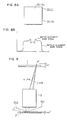
- Fig. 9 shows a relation between image formation at the exposure wavelength of a focusing
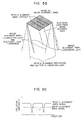
lens 3 of a semiconductor exposure apparatus and image formation at the alignment wavelength. When a wafer is at a position 2', a point P of arecticle 1 is sharply formed on the wafer by the exposure light (g-line) or dotted line light. However, where thealignment lights 521 and 522 (e-line) are obliquely directed to the wafer alignment mark for aligning the wafer and the wafer is at the position 2', the wafer alignment mark image is formed by the focusinglens 3 at a position P' which is displaced from the position P by Δz. In order to resolve this problem, it has been required to lower the level of the wafer from the position 2' to theposition 2 by Δz' to form the pattern of the wafer near the point A on the mask. The distances Δz and Δz' meet the relation of Δz = N²Δz' where N is a magnification of the lens, and Δz' is approximately 200 µm and Δz is 20 mm when N = 10. If the wafer must be moved up and down by 200 µm for each exposure, the total exposure time for the wafer will be further increased. - Referring to Figs. 10A and 10B, a common principle to embodiments shown in Figs. 10A, 14A and 15A is now explained. An alignment/reflection area section including focusing
patterns 60 and 60' is formed in a scribe area or bonding areas around an exposurepattern area section 11, in adjacent to the exposurepattern area section 11 on themask 1. The focusing pattern may comprise hyperbolas as shown in Fig. 11A or quasi-hyperbolas as shown in Fig. 11B. The pattern comprises a number of hyperbolas or quasi-hyperbolas drawn by shifting a hyperbolar or quasi-hyperbola having a width w in a direction x (direction of a line connecting two focal points of the hyperbola) with a pitch p. A black or hatched area represents a Cr surface and a white area represents a Cr-free glass surface. The Cr surface forms the reflection portion. Further, in Fig. 11B, the width w and the lengths ℓ₁, ℓ₂, ℓ₃, ... of the hatched strips are determined such that they form a group of quasi-hyperbolas which will approximate a group of ideal hyperbolas as much as possible that can be drawn with an electron ray lithography apparatus. When amonochromatic light 502 of a wavelength λ is projected to this pattern at incident angle ϑ₀ which is near to 0°, a reflected and diffracted light is condensed into a slit shape at aposition 1122, as shown in Fig. 12A. On the other hand, the alignment mark 22 (or 22'), in Fig. 10, in the scribe area on the wafer or the bonding area in the chip is obliquely illuminated by thee-lines scattered light 503 is transmitted through theimaging lens 3 and the image is focused at the position P' in Fig. 9, directed to the alignment/reflection area section 60 along thelight paths 503 and 503' of Fig. 12A, normally reflected (without diffraction) and focused at theposition 1122. Thus, as shown in Fig. 12B, the focusing pattern is formed such that thearea 60 and the focusingposition 1122 are spaced by Δz from each other. Fig. 12C is a view looked in a normal direction of the drawing in Fig. 12B. Fig. 13 shows the slit-shaped condensed image (Fig. 13C) by the diffraction light from the alignment/reflection area section formed in the vicinity of theposition 1122 and the image (Fig. 13b) formed by obliquely illuminating thechip 21, transmitting the light therefrom through the focusinglens 3 and normally reflecting the light by the Cr surface of the alignment/reflection area section 60. As shown in Figs. 13a and 13b, the image from thechip 21 includes two peaks because of the scattered light created by the edges of the mark 22 (22'). Since a mid-point of the two peaks is a center of the mark 22 (22'), Δx determined in a manner shown in Fig. 13d represents a positional deviation of the pattern. Accordingly, the deviation is focused onto thealignment detector 50 shown in Fig. 10A by themirror 53 and the enlarging focusinglens 52 through thelight path 504 shown in Figs. 10A and 10B so that an alignment control signal corresponding to the deviation is produced. Thewafer 2 or themask 1 is finely moved in accordance with the control signal so that the mask is perfectly aligned with the wafer. Generation of an alignment control signal and attainment of the alignment may be possible in the same manner as in Fig. 5A embodiment. Immediately after the alignment is detected, the exposure light (e.g. g-line) is emitted from the exposure light source means 4 so that the alignment and the exposure are carried out without a time lag and the total wafer exposure time is reduced. - To summarize the principle described above, when the exposure pattern area section on the mask is to be projected onto the surface of the semiconductor wafer which is the workpiece, the alignment/reflection area section having the focusing pattern is arranged on that surface of the mask which does not face the exposure light source, in adjacent to the exposure pattern area section, the image of the reflected diffraction light created by illuminating the focusing pattern with the monochromatic light is detected as the reticle alignment mark image, the image of the alignment mark on the workpiece formed by the scattered light transmitted through the exposure or projection lens is detected and the alignment of those images is attained by driving the means for moving the mask or wafer.
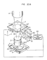
- Referring again to Figs. 10A and 10B, an embodiment will be explained. As shown in Fig. 10B, the mask (reticle) 1 has the exposure pattern area section including the
area 11 and has the alignment/reflection areasections including areas 60 and 60' each carrying the focusing patterns, the alignment/reflection area sections being arranged on that surface of themask 1 which does not face the exposurelight source 4, at a position corresponding to the scribe area. The focusing pattern comprises hyperbolas or quasi-hyperbolas as shown in Fig. 11A or Fig. 11B. As shown in Fig. 12B, the hyperbolas are oriented such that they project toward the circuit pattern. Theareas 60 and 61' may be rectangles having one side of 0.5 - 1 mm long and they are illuminated by a parallel beam of a He-Nelaser beam source 51 through a mirror 54 (Since the illumination and detection systems for the area 60' are identical to those for thearea 60, they are not shown.) The He-Ne laser beam diffracted by the focusing pattern is condensed into a slit shape at theposition 1122 shown in Fig. 10B. On the other hand, thechip 21 to be exposed is on the wafer on themovable wafer stage 7 and under the lens and at a position slightly deviated from the exact wafer position. The chip already has had the alignment mark formed in the scribe area, and if this mark aligns with the focusing pattern of the alignment/reflection area 60 of the mask, the mask pattern can be precisely overexposed on the chip. Thus, the alignment mark on the scribe area of thewafer 2 is focused at 1122 by obliquely illuminating the alignment mark by the He-Ne laser beams 521 - 524 in four directions, transmitting the lights scattered by the edges of the alignment mark through the focusinglens 3 and normally reflecting the lights by the reflection portion of thearea 60, that is, the Cr surface of the focusing pattern. The alignment mark image from the wafer formed at 1122 and the condensed image formed by the reflection and diffraction of the light from the mask are enlarged and focused on a detection plane (not shown) of thealignment detector 50 by themirror 53 and the enlarging focusinglens 52 to determine the registration of both alignment mark images. The detection may be made by a solid-state imaging device or a combination of a scanning slit and a photo-multiplier. Misregistration of both patterns is detected and the control signal is generated. Thewafer stage 7 or themask 1 is moved in accordance with the control signal, and when the registration is attained, the exposure is carried out. Since theexposure light 41 is completely isolated from the alignment optical system and does not interfere, the exposure is completed immediately after the alignment. - Figs. 14A and 14B show another embodiment of the present invention. The like elements to those shown in Figs. 10A and 10B are designated by the like numerals. In Figs. 14A and 14B, the focusing patterns in the
areas 60 and 60' of the alignment/reflection area sections adjacent to the exposure pattern areasection including area 11 of themask 1 are arranged at free locations in the bonding area in the exposure pattern area. The light from the e-line illumination light source 51'' of the mercury lamp is transmitted through thesemitransparent mirror 56 along thelight path 501, normally reflected by the reflection portion of the alignment/reflection area 60 including the focusing pattern such as that shown in Figs. 11A and 11B, and transmitted through the focusinglens 3 to illuminate thealignment patterns 22 and 22' in the bonding area of thechip 21. The scattered (reflection) light again returns to thelight path 503, again normally reflected by the reflection portion of thearea 60 and focused at 1122 (Fig. 14B). The mask position may be determined by directing themonochromatic light 502 emitted from the He-Ne laser beam source, an Ar laser beam source or the e-line light source 51' to the alignment/reflection area 60 through themirror 54 and detecting the slit-shaped image at 1122 by the diffraction light from the focusing pattern. The detection of the alignment mark images of themask 1 and thewafer 2 and the alignment control are identical to those described in the above embodiment. - Figs. 15A and 15B show another embodiment of the present invention. The like elements to those shown in Figs. 10A and 10B are designated by the like numerals. The light emitted from the semiconductor laser 51'' obliquely illuminates the alignment/
reflection area 60 on themask 1. Since the wavelength of the light is long, a primary diffraction angle is large and the primary diffracted light is returned in the incident direction and focused into a slit shape atposition 1122. On the other hand, the light normally reflected by the reflection portion of thearea 60 including the pattern as shown in Figs. 11A and 11B is transmitted along the light path 503' and used to illuminate the alignment mark in the scribe area of the wafer. The alignment mark of the wafer may be obliquely illuminated by the laser beams 521 - 524 in four directions, and the scattered light created by the step of the alignment mark of the wafer or the reflection light created by the illumination is normally reflected by the reflection portion of thearea 60 and focused at 1122 as may be done in the previous embodiment. The detection of the signals of the alignment mark images of the mask and the wafer and the alignment control are now explained. - In the embodiments shown in Figs. 10A, 14A and 15A, it is desirable that the position corresponding to the alignment mark in the scribe area or the bonding area of the chip is not illuminated during the exposure step. Accordingly, it is desirable to arrange a blade for restricting the exposure area above the mask although it is not shown in the drawing of the embodiment.
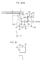
- Fig. 16 shows another arrangement of the alignment/reflection area section formed on the mask. It is particularly suitable for use in the exposure apparatus shown in Fig. 5A although it may be used in the exposure apparatus shown in other drawings.
- As shown in Fig. 17A, the alignment/
reflection area section 61 has a reflection portion 61-1a at a center of the pattern and an alignment portions 61-1b including a focusing pattern at its side peripheries. The focusing pattern comprises a group of curves drawn by shifting a portion of a hyperbola in y-direction at a constant pitch, that is, a pattern of a group of hyperbolas. In order to form such a pattern on the mask, an electron beam lithography apparatus is usually used. When the pattern is fine, it is difficult to smoothly draw a curved pattern. Accordingly, small rectangles having sides along the x-direction and y-direction may be arranged to simulate the hyperbola. - The alignment/
reflection area section 61 shown in Fig. 16 is arranged in the same manner as the alignment/reflection area 60 shown in Fig. 5A is arranged to align the wafer with the mask. However, the alignment light has a wavelength different from that of the exposure light, unlike in Fig. 5A embodiment. Referring again to Fig. 5A, the wafer alignment mark is illuminated by directing the laser illumination light 501' through thegalvanomirror 53, thebeam splitter 55, the focusinglens 52 and the mirror orbeam splitter 51 to the reflection portion 61-1a (Fig. 16) at the center of the alignment/reflection area 61 on thereticle 1 so that the reflection light is transmitted through thereduction lens 3 and illuminates thewafer alignment mark 22 and the reflection light therefrom passes the same light path and is reflected by thearea 61 to form the waferalignment mark image 1012 as shown in Fig. 16. The position of the image formed is determined by the wavelength of the laser beam 501' used for the alignment and a chromatic aberration of thereduction lens 3. The surfaces of the mask (reticle) and the wafer are in the focusing relation for the exposure light by the reduction lens, but the image of the alignment mark on thewafer 2 is not formed on the area on the lower surface of the mask (reticle) 1 by the alignment detection light and it is reflected by thearea 61 and focused at 1012 which is spaced from the lower surface of the mask by distance h. In the present embodiment, in order to detect the relative position of the wafer and the mask (reticle) by the wafer alignment mark image, the alignment/reflection area 61 has the center reflection portion 61-1a and the peripheral alignment mark portions 61-1b which contains the pattern of hyperbolas. When thelaser illumination light 503 is irradiated to the pattern 61-1b, thelinear image 1122 is formed at the position of the image of the wafer alignment mark. A shape of the hyperbolas and a strength distribution of the linear image (change in the x-direction) for forming the linear image at the focusing positon of the wafer alignment mark (spaced from the lower surface of the reticle by h) are now explained with reference to Figs. 17A - 17C. - Fig. 17A shows the alignment/
reflection area 61 on thereticle 1 and coordinates (x, y) exist on this plane. The mask alignment marks 61-1b which include the focusing patterns, that is, the hyperbola patterns (hyperbola gratings) are arranged on the opposite sides of the reflection portion 61-1a. Broken lines shown in the reflection portion 61-1a merely show connections of the left and right hyperbolas and they are not real patterns. Figs. 17B and 17C are side views of Fig. 17A, and x-y coordinates and y-z coordinates exist on the respective planes. The incident laser beam is a collimated beam which is in the y-z plane, makes an angle ϑ₀ with the z-axis, is reflected and diffracted by the pattern of hyperbolas arranged at a pitch p to form thelinear pattern 1122 at the position spaced from the lower surface of the reticle by h. The optical axis of the diffraction light makes an angle ϑ₁ with the z-axis. The pattern of hyperbolas is represented by the following formula.
where n is an integer. It is an aggregation of hyperbolas whose asymptotic curve is given by the following formula.
The pitch p of the hyperbolas is given by
This hyperbola grating (hyperbola pattern) does not exist in the reflection portion 61-1a as shown in Fig. 17A (broken lines) but exists in the alignment mark portions 61-1b on the opposite sides of the reflection area 61-1a. A width of the reflection portion 61-1a is represented by Wm and a total width of the hyperbola pattern (including the width of the reflection portion 61-1a) is represented by Wg. The width Wm should be at least a width of the illumination beam for the wafer alignment mark. If the reflection portion 61-1a is too narrow and the illumination beam illuminates the hyperbola pattern, the reflected diffraction light therefrom is superimposed on the wafer alignment mark and an S/N ratio of a detection signal for the wafer alignment mark is reduced. The width is approximately equal to a product of a diameter of an illumination area necessary to detect the wafer alignment mark and a reciprocal of a reduction factor of the reduction lens. When the collimated laser beam having the wavelength λ is applied to the hyperbola pattern represented by the formula (1) having the width Wg and the center blank portion Wm, at the incident angle ϑ₀, the reflected diffraction beam forms the linear image extending along the y-axis at the position spaced from the mask surface by h, as shown in Figs. 17B and 17C. An intensity distribution I(X) in the x-direction (coordinate on the linear image is X) is given by
where
C is a constant proportional to a laser beam intensity and a reflection factor.
It is a pattern of a square of cosine waves having zero phase at a center of the pattern and having an envelope represented by Ie² as shown by a broken line in Fig. 18. Because the linear pattern has a symmetric fine structure, the center of the pattern can be precisely determined so that the position of the mask can be precisely determined. As described above, this pattern is formed on the same focusing plane (h below the reticle surface) as that of the wafer alignment mark image formed by illuminating the wafer alignment mark by the laser beam and enlarging the image by the reduction lens (after the reflection by the reflection portion of the alignment/reflection area). Accordingly, as shown in Fig. 5A, it can be detected by the same detection system as that for the wafer alignment mark, by using the solid-state array device 50 through themirror 51, focusinglens 52 andbeam splitter 55. Accordingly, a drift of the detection position with time is zero as compared with a case where the marks are detected by two separate detection optical systems, and the optical system can be simplified and rendered inexpensive. The wafer target alignment mark and the diffraction image of the hyperbola pattern representing the reticle position are time-serially detected by the same detection system. As shown in Fig. 5A, thewafer 2 is moved by the array pitch of the chip by the x-y movable stage (wafer table) 7 so that an unexposed chip is brought under the reduction lens. The wafer alignment mark illumination laser beam 501' first illuminates thewafer alignment mark 22 so that the position thereof is detected by the solid-state array device 50. Then, the laser beam 501' is extinguished and theillumination light 503 illuminates the alignment/reflection area (hyperbola pattern) on the reticle so that the reticle position is detected by the solid-state array device 50. A relative deviation is determined based on the two detected positons and it is compensated by finely adjusting thereticle 1 by the reticle (mask)fine adjusting mechanism 130. Since the distance of fine adjustment is the product of the reciprocal of the reduction factor of the reduction lens and the distance of the relative movement of thewafer 2, precise positioning is attained as compared to a case where thewafer 2 is moved. Since the positions of the wafer and the mask are time-serially detected, both detection patterns can be independently detected and the S/N ratio is not lowered by the other pattern. Thus, high precision detection is attained. - As shown in Figs. 17A to 17C, the collimated laser beam is irradiated to the alignment/
reflection area 61 at the incident angle ϑ₀ when the reticle position is to be detected, but the light normally reflected by thearea 61 is transmitted through thereduction lens 3 and illuminates the wafer alignment mark. As a result, the wafer alignment mark image may be superimposed on the diffraction linear image of the hyperbola pattern. This does not pose a substantial problem when the intensity of the diffraction linear image is high, but the influence of the superposition on the alignment precision cannot be neglected if the intensity of the reflection image of the wafer alignment mark is high or an extremely high alignment precision is required. - A resolution to this problem is discussed below.
- The width Wm of the reflection portion 61-1a of the
area 61 shown in Figs. 17A to 17C is selected to a minimum required to illuminate the wafer alignment mark, and the width Wg is selected to
where NA is the number of aperture of the detection optical system. In this manner, Wg-Wm is selected to be large. As a result, a peak of the intensity of the hyperbola grating diffraction image (Fig. 18) is proportional to (Wg-Wm)² and the reduction of the S/N ratio due to the superposition of the wafer pattern image is avoided. - In a second solution, the recticle pattern of Fig. 16 does not use the conventional Cr mask but uses the Cr₂O₃ mask. A reflection factor rcr of the Cr mask for the wavelength λ = 500 nm is approximately 60% while a reflection factor

of the Cr₂O₃ mask is approximately 16%. The intensity Iw of the wafer alignment mark image is proportional to r² because the light is reflected twice in the illumination cycle and the imaging cycle. On the other hand, the intensity Im of the hyperbola pattern diffraction image representing the reticle position is proportional to r because the diffraction image is obtained by one reflection by the mask. Accordingly, a ratio of the intensity of the mask alignment mark diffraction image and the intensity of the wafer alignment mark image (noise image in detecting the mask alignment mark diffraction image), that is, the S/N ratio is given by
Accordingly, the smaller the mask reflection factor is, the higher is the S/N ratio. The S/N ratio when the Cr₂O₃ mask is used is approximately four times as large as that when the Cr mask is used. Other low reflection factor materials than Cr₂O₃ may be used to attain the same effect. The effect will be satisfactory if the S/N ratio is at least three times as high as that obtained when the Cr mask is used. - A third solution is shown in Figs. 19A - 19C. If the laser beam is irradiated only to the hyperbola pattern 61-1b on the opposite sides of the reflection portion 61-1a of the alignment/
reflection area 61 and not irradiated to thewafer alignment mark 22, the wafer alignment mark image is not superimposed as the noise. As shown in Figs. 19A - 19C, arestrictive illumination mask 540 is inserted in the light path of the collimatedillumination light beam 503 so that only the alignment mark portion 61-1b of thearea 61 on thereticle 1. As shown in Fig. 19B, themask 540 transmits the light in the area (openings) corresponding to the hyperbola pattern area and blocks the light in other areas. The collimated light transmitted through the restrictive illumination mask passes throughlenses area 61 on thereticle 1. Fig. 19C illustrates how thearea 61 in Fig. 19A is illuminated by the light 503 masked by themask 540. As can be seen, only the alignment portions 61-1b carrying hyperbolic patterns receive light 5401' representative of the images of theopenings 5401. With this arrangement, since the reflection portion 61-1a is not illuminated, the intensity of light undesirably reaching the wafer alignment mark is so small that the reticle position can be detected with a high signal-to-noise ratio. - A fourth solution is described below. The focusing position of the wafer alignment mark image and the position of the diffraction image of the hyperbola pattern representing the reticle position are intentionally shifted from each other on the focusing plane. The amount of shift depends on the alignment precision in the step-and-repeat process of the wafer table and is to be larger than the line width of the wafer alignment mark. The mark or pattern is formed such that the wafer alignment mark and the diffraction image of the hyperbola pattern representing the reticle position are relatively shifted from each other by the above shift amount. Alternatively, the illumination light for the hyperbola pattern may be slightly shifted from the right angle by an angle made thereby with the x-axis as shown in Figs. 17A and 17C.
- In the above embodiments, when the exposure pattern is to be projected to the wafer, the g-line, e-line and d-line which are spectrum lines of the mercury lamp or the He-Ne laser beam is used to align the patterns of the mask and the wafer. Such a light is irradiated through the exposure focusing lens. Since the exposure focusing lens is usually designed to exhibit a best focusing characteristic (high resolution power) only to the monochromatic light such as g-line, the spectrum width of the illumination light other than the exposure light must be narrow. However, for the light other than the exposure light, the focusing position on the optical axis varies significantly even for a slight change of the wavelength. Accordingly, in order to attain the alignment detection pattern with a high resolution, it is necessary to use the light of as narrow spectrum width as possible. However, the light source other than the laser, such as the mercury lamp cannot produce a light having a sufficiently narrow spectrum width and a sufficient intensity to allow the detection of the alignment mark on the wafer. Accordingly, it is advantageous to use the laser beam as the alignment light source from the standpoints of intensity and resolution. However, since the laser beam usually has a high coherence (spatial coherence), if the alignment mark on the wafer is marked by granular material such as Al or WSi, a noise called a speckle pattern is included in the mark image detection signal and the S/N ratio of the detection signal is lowered. By multiple interference created between the surface of the resist layer coated on the wafer to be aligned and the alignment mark or the underlying layer carrying the alignment mark, a fine variation of the thickness of the resist layer may appear as a noise so that the S/N ratio of the detection signal is lowered.
- Referring to Figs. 20A and 20B, an exposure apparatus and an alignment method according to an embodiment of the present invention which suppresses the speckle pattern noise and the multiple interference will be explained. The alignment light has a wavelength different from that of the exposure light.
- Alignment/reflection area
sections including areas 30 and 30' on the mask (reticle) 1 may contain the focusing patterns shown in Figs. 10A, 10B, 11A, 11B, 12A-12C and 13 and may be arranged on themask 1 in the manner shown in those figures.Numeral 4 denotes an exposure light source. The light emitted from thelaser beam source 90 is split by thebeam splitter 91. One of the split beams illuminates the alignment/reflection area 30 containing the hyperbola pattern. The illumination light is diffracted and a primary diffraction light passes through alight path 601 and focused into a linear image at 600. The direction (x-direction) of the linear image represents the x-direction of thereticle 1. The other of the split beams is deflected by aGalvanomirror 92 which is an incident angle varying means. The deflected beam passes through asemitransparent mirror 83, alens 84 and amirror 85 and is directed to the alignment/reflection area 30 adjacent to theexposure pattern area 11 of the mask (reticle) 1, and the normally reflected light therefrom is directed into anentrance pupil 205 of theexposure focusing lens 3. The light 612 transmitted through the entrance pupil illuminates the alignment mark 22 (22') on the wafer arranged in the periphery of thechip 21 on thewafer 2. Thechip 21 on thewafer 2 includes the elongated alignment marks 22 and 22' extending in the y-direction and the x-direction as shown in Fig. 21. In Figs. 20A and 20B, only a control unit including an optical system for aligning thealignment mark 30 on thereticle 1 with thealignment mark 22 on thewafer 1 is shown as the alignment optical system, and another control unit including an optical system for aligning the mark 30' with the mark 22' is omitted because it may be identical. The laser beam directed to thealignment mark 22 on thewafer 1 in Figs. 20A and 20B has no change of incident angle in the x-z plane (x-direction) normal to the lengthwise direction of the alignment mark as shown in Fig. 22B, but the incident angle changes in the y-z plane (y-direction) normal to themask 1 or thewafer 2 as shown in Fig. 22C. Fig. 22B shows a view of thealignment mark 22 on the wafer 2 (underlying layer of the alignment mark) as viewed in a direction A shown in Fig. 22A, and Fig. 22C is a view as viewed in adirection B. Numeral 43 in Figs. 22B and 22C denotes a resist film coated on thewafer 2. - The light including the position information of the
alignment mark 22 reflected by thewafer 2 is usually a diffraction pattern spreading in a direction (x-direction) normal to the lengthwise direction (y-direction) of the alignment mark on thewafer 1, as shown by 220, 221 and 222 in Fig. 23A, on theentrance pupil 205 of the exposure focusing lens 3 (x-y plane parallel to themask 1 or the wafer 2). Accordingly, by deflecting the incident angle to the y-direction (normal to the x-axis) in the y-z plane as shown in Fig. 22C, the diffraction light information, particularly the position information of the pattern to be detected (x-coordinate for thealignment mark 22 and y-coordinate for the mark 22') can be detected without loss. For comparison purpose, Fig. 23B shows the light deflected in the normal direction (x-direction in the z-x plane). In this case, the information in the direction to be detected is lost. The incident light is deflected in the direction shown in Figs. 22A - 22C and 23A, reflected by thewafer 2, again passes through theentrance pupil 205 of the focusinglens 3, normally reflected by the reflection portion of the alignment/reflection area 30 on thereticle 1 and the image of the alignment mark of the wafer is focused at 600 at which the linear image of the diffraction light from the reticle is focused (reticle alignment mark image). The reticle alignment mark image and the wafer alignment mark image are transmitted through themirror 85,lens 84 andbeam splitter 83 and refocused on the imaging plane of the imaging means 81 by the focusing optical system 82. - The noise superimposed on the wafer alignment mark and the suppression of the noise are now explained. The wafer
alignment mark image 22 and the maskalignment mark image 30 focused on the imaging plane of the imaging means 81 are shown in Fig. 25, in whichnumeral 600 denotes the imaging plane, numeral30 denotes the image of thereticle window 30, and numeral22 denotes the image of thealignment mark 22 of thewafer 2. When a two-dimension array solid-state imaging device is used as the imaging means 81, a light intensity It(i, j) is detected at time t for an address (i, j) of the array pixels. The detection signals in the longitudinal direction of thealignment mark 22 are summed.
so that the signals are averaged and the S/N ratio is improved. When the alignment mark of thewafer 2 is marked by granular material such as aluminum, the S/N ratio of the detection signal is still low even after the averaging as shown in Figs. 26A and 26B, in which the incident angles of the illumination light are fixed at different angles. As shown in Fig. 24, the incident angle ϑ is changed from time to time in the plane described above. During the change of the incident angle (to - tN)t the image information is accumulated. Consequently, the detection signal in the i-direction OΣ(i) is now represented by the following expression:
Since the accumulation is usually done in the conventional imaging means, no special means is required. An image read-in period T₁ (normally 16 ms) and a deflection period T₂ by the Galvanomirror meet a relation of T₁ = n₀T₂ (where n₀ is an integer). Thus, the information in Figs. 26A, 26B, ... are averaged and a high S/N signal as shown in Fig. 26C is produced. Accordingly, the alignment mark difficult to detect, such as the aluminum alignment mark can be detected. - Figs. 27A - 27C show other modes of changing the incident angle to the wafer alignment mark. In Fig. 27A, the incident angle is set by a step function, and in Figs. 27B and 27C, the incident angles are fixed depending on the alignment marks.
- Figs. 28A and 28B illustrate the illumination of the alignment mark in the multiple interference environment. When the multiple interference occurs between the resist
surface 43 and thealignment mark 22 or theunderlying layer 2, the interference intensity is determined by an optical path difference Δℓ = 2ndcosϑ of the layer and a complex index of refraction of the resist, alignment mark or underlying layer. Normally, it periodically changes with the film thickness d as shown in Fig. 29 (λ = 514 nm). When an average resist layer thickness dm is 1.6 µm ±0.14 µm, the interference intensity significantly changes (ΔOϑ=0°) at ϑ = 0°. When ϑ = 13°, the interference intensity changes with d as shown by a broken line and the change is small (ΔOϑ=13°). At the edge of the wafer alignment mark, the signal intensity changes as shown in Figs. 30A, 30B and 30C (which show the intensities detected in the x-direction when the resist layer thickness changes only depending on the shape of the underlying layer and is symmetric, or changes in accordance with the edge of the pattern). The signal ΔO is superimposed as the noise on the signals of Figs. 30A - 30C so that misdetection of the edge may occur when ΔO is large. By adjusting the incident angle to an optimum angle, the detection with a high S/N is attained. - In Fig. 31, IR denotes the reticle alignment mark image and IW denotes the wafer alignment mark image. A deviation between the centers of those signal waveforms is detected by the
detection system 80 and the wafer table 7 is moved in the x-direction (and also in the y-direction) to compensate for such deviation. As shown in Fig. 20B (not shown in Fig. 20A),shutters - In the embodiments described hereinbefore, use is made of a two-dimensional imager means such as a solid-state camera to detect images of wafer alignment marks and reticle alignment marks. However, since these images carry only one-dimensional information, detection of these images is possible at a high speed and with a high resolution by the provision of a cylindrical lens before the imager means for compressing the lengthwise information of the images of the elongated or slender alignment marks and by the use of a one-dimensional array of imaging elements (e.g. CCD) for the imager means. The cylindrical lens and one-dimensional array may be, e.g., those disclosed in printed Japanese publications, Japanese Patent Publication No. 29045/83 or 53217/81.
- As described hereinabove, in accordance with the present embodiment, the alignment mark on the wafer is illuminated by the laser beam having the narrow spectrum width so that the defocusing due to the chromatic aberration of the exposure focusing lens is minimized and the level of the detection signal is kept sufficiently high. Further, the incident angle of the laser beam can be controlled to an optimum angle in accordance with the semiconductor process such as the material of the resist layer, the thickness thereof, the shape of the underlying layer and the material thereof so that the noise due to the coherence of the laser beam is substantially reduced. Accordingly, the stability of the detection of the alignment pattern is significantly improved.
and is characterised in
that said alignment area section further includes both a reflection and a diffraction portion,
that said exposure pattern area section and said alignment area section are disposed on that surface of said mask plate means which does not face said first light source means
and
that said alignment means includes second light source means arranged with respect to said mask plate means such that light from said second light source means is directed to illuminate said mask alignment mark and said workpiece alignment mark so that the resulting reflected light from said workpiece alignment mark is directed to said alignment area section through said projection lens means and is reflected at said reflection portion to provide a reflection image of said workpiece alignment mark and detecting means for detecting said reflection image of said workpiece alignment mark and an image of said mask alignment mark portion of said alignment area section to produce said control signal.
and is characterised in
that for said illuminating step said alignment area section is arranged so as to be adjacent to said exposure pattern area section on that surface of said exposure mask plate which does not face said first light source means, said alignment area section including an alignment mark portion and a further portion comprising reflecting and diffracting parts
and
that said illumination of said alignment area section of said mask plate and of said workpiece alignment mark is carried out with second light source means so that light reflected at said workpiece alignment mark passes through said projection lens means and is reflected at said reflecting part of said further portion including reflecting and diffracting parts.
Claims (16)
- An exposure apparatus, comprising- first light source means (4);- mask plate means (1)
having an exposure pattern area section (11) and an alignment area section (30, 30') adjacent to said exposure pattern area section and including a mask alignment mark portion
and
being arranged so that said exposure pattern area section is illuminated by said first light source means;- movable stage means (7) for thereon holding a workpiece (2) having a workpiece alignment mark (22, 22');- projection lens means (3)
interposed between said mask plate means and said movable stage means
and
disposed across said mask plate means from said first light source means so that said exposure pattern area section, when illuminated, is projected onto said workpiece through said projection lens means;- alignment means
for detecting the positional relation between said mask alignment mark portion of said alignment area section in said mask plate means and said workpiece alignment mark of said workpiece on said movable stage means
and
for producing a control signal for achieving alignment of said mask alignment mark portion with said workpiece alignment mark
and- driving means
destined for adjusting the relative position between said mask plate means and said workpiece
and
adapted to be responsive to said control signal;
characterised in
that said alignment area section (30, 30') further includes both a reflection and a diffraction portion,
that said exposure pattern area section and said alignment area section are disposed on that surface of said mask plate means which does not face said first light source means (4),
and
that said alignment means includes(a) second light source means (503; 521 to 524; 51''; 90) arranged with respect to said mask plate means such that light from said second light source means is directed to illuminate said mask alignment mark and said workpiece alignment mark so that the resulting reflected light from said workpiece alignment mark is directed to said alignment area section through said projection lens means (3) and is reflected at said reflection portion to provide a reflection image of said workpiece alignment mark and(b) detecting means (5; 50, 52, 54, 56; 80 to 85) for detecting said reflection image of said workpiece alignment mark and an image of said mask alignment mark portion of said alignment area section to produce said control signal. - An apparatus according to claim 1,
characterised in
that the wavelength of the light from said second light source means (503) is substantially equal to that of the light from said first light source means (4)
and
that said alignment area section (30, 30') has a predetermined contour. - An apparatus according to claim 2,
characterised in
that said contour of said alignment area section (30, 30') constitutes said mask alignment mark portion. - An apparatus according to claim 2,
characterised in
that said alignment area section (30, 30') includes grating means constituting said mask alignment mark portion. - An apparatus according to claim 1,
characterised in
that the wavelength of the light from said second light source means (521 to 524) is different from that of the light from said first light source means (4)
and
that said alignment area section (30, 30') includes a group of substantially hyperbolic lines (60) for forming a diffraction image representative of said mask alignment mark portion. - An apparatus according to claim 5,
characterised in
that said group of hyperbolic lines (60) is oriented to project light towards said exposure pattern area section in said mask plate means (1). - An apparatus according to claim 1,
characterised in
that the wavelength of the light from said second light source means (521 to 524) is different from that of the light from said first light source means (4),
that said mask alignment mark portion consists of first and second alignment sub-portions (61-1b) with said reflective portion (61-1a) being interposed therebetween
and
that first and second alignment sub-portions carry parts of a group of hyperbolic lines for providing, when illuminated, an image representative of said mask alignment mark portion. - An apparatus according to claim 1,
characterised in
that said alignment means further includes(c) means (92) optically coupled with said second light source means (90) for changing the incidence angle of the light illuminating said workpiece alignment mark (22, 22') in a plane perpendicular to said mask plate means (1) and parallel to the lengthwise direction of said workpiece alignment markand
that said detecting means include means for accumulating reflected light from said workpiece alignment mark received via said reflection portion of said alignment area section (30, 30'). - An apparatus according to claim 1,
characterised in
that said second light source means (521 to 524) is positioned so as to emit light able to illuminate said workpiece alignment mark obliquely without passing said projection lens means (3). - An apparatus according to claim 1,
characterised in
that said second light source means (503; 51''; 90) is positioned so as to direct light first to said alignment area section (30; 60) to be reflected at the reflective portion thereof and to be directed through said projection lens means (3) to said workpiece alignment mark (22, 22') to thereby illuminate said workpiece alignment mark. - A method of aligning an exposure mask plate (1) with a workpiece (2) having a workpiece alignment mark (22, 22') in an exposure apparatus in which the exposure mask plate includes an exposure pattern area section and an alignment area section and said exposure pattern area section is illuminated by first light source means (4) to project images of patterns contained in an exposure pattern area section (11) through projection lens means (3) onto the workpiece (2) being held on movable stage means (7), said method comprising the steps of:- illuminating said alignment area section of said mask plate and said workpiece alignment mark (22, 22');- detecting the positional relation between said alignment mark portion and said workpiece alignment mark;- producing a control signal representative of misregistration between said alignment mark portion and said workpiece alignment mark derived from the detected positional relation;
and- adjusting the relative position between said exposure mask plate and said workpiece in accordance with said control signal,characterised in
that for said illuminating step said alignment area section (30; 60) is arranged so as to be adjacent to said exposure pattern area section on that surface of said exposure mask plate (1) which does not face said first light source means (4), said alignment area section including an alignment mark portion and a further portion comprising reflecting and diffracting parts,
and
that said illumination of said alignment area section of said mask plate and of said workpiece alignment mark is carried out with second light source means (503; 521 to 524; 51'';90) so that light reflected at said workpiece alignment mark passes through said projection lens means (3) and is reflected at said reflecting part of said further portion including reflecting and diffracting parts. - A method according to claim 11,
characterised in
that during the step of illuminating said workpiece alignment mark the incidence angle (0) of the light illuminating said workpiece alignment mark (22, 22') is varied in a plane perpendicular to said exposure mask plate (1) and parallel to the lengthwise direction of said workpiece alignment mark. - A method according to claim 11,
characterised in
that light for illuminating said workpiece alignment mark (22, 22') is caused to pass through said projection lens means (3). - A method according to claim 11,
characterised in
that light for illuminating said workpiece alignment mark (22, 22') is directed thereto without passing through said projection lens means (3). - A method according to claim 11,
characterised in
that said alignment mark portion includes a grating pattern and
that said second light source means (521 to 524; 51''; 90) is capable of emitting a substantially monochromatic light having a wavelength different from that of the light from said first light source means (4). - A method according to claim 15,
characterised in
that said grating pattern is formed by a group of substantially hyperbolic lines (60).
Applications Claiming Priority (4)
| Application Number | Priority Date | Filing Date | Title |
|---|---|---|---|
| JP243866/83 | 1983-12-26 | ||
| JP58243866A JPH0612753B2 (en) | 1983-12-26 | 1983-12-26 | Pattern detection method and apparatus thereof |
| JP59222010A JPS61100931A (en) | 1984-10-24 | 1984-10-24 | Method of exposing semiconductor |
| JP222010/84 | 1984-10-24 |
Publications (3)
| Publication Number | Publication Date |
|---|---|
| EP0148477A2 EP0148477A2 (en) | 1985-07-17 |
| EP0148477A3 EP0148477A3 (en) | 1985-09-04 |
| EP0148477B1 true EP0148477B1 (en) | 1991-09-04 |
Family
ID=26524628
Family Applications (1)
| Application Number | Title | Priority Date | Filing Date |
|---|---|---|---|
| EP84115889A Expired - Lifetime EP0148477B1 (en) | 1983-12-26 | 1984-12-20 | Exposure apparatus and method of aligning exposure mask with workpiece |
Country Status (4)
| Country | Link |
|---|---|
| US (1) | US4668089A (en) |
| EP (1) | EP0148477B1 (en) |
| KR (1) | KR900001269B1 (en) |
| DE (1) | DE3485022D1 (en) |
Families Citing this family (46)
| Publication number | Priority date | Publication date | Assignee | Title |
|---|---|---|---|---|
| US4937618A (en) * | 1984-10-18 | 1990-06-26 | Canon Kabushiki Kaisha | Alignment and exposure apparatus and method for manufacture of integrated circuits |
| US4828392A (en) * | 1985-03-13 | 1989-05-09 | Matsushita Electric Industrial Co., Ltd. | Exposure apparatus |
| JPH0616480B2 (en) * | 1985-06-03 | 1994-03-02 | 株式会社日立製作所 | Reduction projection type alignment method and apparatus |
| US4771180A (en) * | 1985-10-11 | 1988-09-13 | Matsushita Electric Industrial Co. Ltd. | Exposure apparatus including an optical system for aligning a reticle and a wafer |
| JPH0685387B2 (en) * | 1986-02-14 | 1994-10-26 | 株式会社東芝 | Alignment method |
| JPH0785466B2 (en) * | 1986-07-04 | 1995-09-13 | キヤノン株式会社 | Positioning device |
| US4943733A (en) * | 1987-05-15 | 1990-07-24 | Nikon Corporation | Projection optical apparatus capable of measurement and compensation of distortion affecting reticle/wafer alignment |
| JPH065663B2 (en) * | 1987-06-30 | 1994-01-19 | 株式会社日立製作所 | Semiconductor exposure method and apparatus |
| JPH01189503A (en) * | 1988-01-25 | 1989-07-28 | Hitachi Ltd | Method and apparatus for detecting pattern |
| US5340992A (en) * | 1988-02-16 | 1994-08-23 | Canon Kabushiki Kaisha | Apparatus and method of detecting positional relationship using a weighted coefficient |
| US5260771A (en) * | 1988-03-07 | 1993-11-09 | Hitachi, Ltd. | Method of making semiconductor integrated circuit, pattern detecting method, and system for semiconductor alignment and reduced stepping exposure for use in same |
| US5094539A (en) * | 1988-03-07 | 1992-03-10 | Hitachi, Ltd. | Method of making semiconductor integrated circuit, pattern detecting method, and system for semiconductor alignment and reduced stepping exposure for use in same |
| US5155370A (en) * | 1988-09-09 | 1992-10-13 | Canon Kabushiki Kaisha | Device for detecting the relative position of first and second objects |
| JP2650396B2 (en) * | 1989-02-07 | 1997-09-03 | キヤノン株式会社 | Position detecting device and position detecting method |
| JPH032504A (en) * | 1989-05-30 | 1991-01-08 | Nikon Corp | Aligning device |
| US5053628A (en) * | 1989-07-13 | 1991-10-01 | Matsushita Electric Industrial Co., Ltd. | Position signal producing apparatus for water alignment |
| FR2656700B1 (en) * | 1989-12-28 | 1992-08-07 | Aerospatiale | METHOD FOR RESTORING THE MOVEMENT OF A MOBILE BY OBSERVING A SYMBOL FORMED THEREON AND DEVICES FOR IMPLEMENTING THE METHOD. |
| US5357311A (en) * | 1991-02-25 | 1994-10-18 | Nikon Corporation | Projection type light exposure apparatus and light exposure method |
| JP3210123B2 (en) * | 1992-03-27 | 2001-09-17 | キヤノン株式会社 | Imaging method and device manufacturing method using the method |
| US5274420A (en) * | 1992-04-20 | 1993-12-28 | International Business Machines Corporation | Beamsplitter type lens elements with pupil-plane stops for lithographic systems |
| KR970003593B1 (en) * | 1992-09-03 | 1997-03-20 | Samsung Electronics Co Ltd | Projection exposure method and device using mask |
| JP3195200B2 (en) * | 1994-12-09 | 2001-08-06 | キヤノン株式会社 | Semiconductor exposure apparatus and foreign matter detection method |
| JP3450509B2 (en) * | 1995-04-13 | 2003-09-29 | キヤノン株式会社 | Projection exposure apparatus and method for manufacturing an element using the apparatus |
| US6270947B2 (en) * | 1999-04-30 | 2001-08-07 | Infineon Technologies Ag | Method and apparatus for reducing non-uniformity area effects in the manufacture of semiconductor devices |
| GB2356786B (en) | 1999-11-29 | 2003-09-03 | Marconi Electronic Syst Ltd | Method and apparatus for aligning a crystalline substrate |
| JP4414535B2 (en) * | 2000-01-13 | 2010-02-10 | 進 野田 | Manufacturing method of semiconductor device |
| US6700096B2 (en) * | 2001-10-30 | 2004-03-02 | Semiconductor Energy Laboratory Co., Ltd. | Laser apparatus, laser irradiation method, manufacturing method for semiconductor device, semiconductor device, production system for semiconductor device using the laser apparatus, and electronic equipment |
| TWI289896B (en) * | 2001-11-09 | 2007-11-11 | Semiconductor Energy Lab | Laser irradiation apparatus, laser irradiation method, and method of manufacturing a semiconductor device |
| TWI291729B (en) * | 2001-11-22 | 2007-12-21 | Semiconductor Energy Lab | A semiconductor fabricating apparatus |
| US7133737B2 (en) * | 2001-11-30 | 2006-11-07 | Semiconductor Energy Laboratory Co., Ltd. | Program for controlling laser apparatus and recording medium for recording program for controlling laser apparatus and capable of being read out by computer |
| JP3949564B2 (en) * | 2001-11-30 | 2007-07-25 | 株式会社半導体エネルギー研究所 | Laser irradiation apparatus and method for manufacturing semiconductor device |
| CN100508140C (en) * | 2001-11-30 | 2009-07-01 | 株式会社半导体能源研究所 | Manufacturing method for a semiconductor device |
| US7214573B2 (en) * | 2001-12-11 | 2007-05-08 | Semiconductor Energy Laboratory Co., Ltd. | Method of manufacturing a semiconductor device that includes patterning sub-islands |
| JP4282985B2 (en) * | 2002-12-27 | 2009-06-24 | 株式会社半導体エネルギー研究所 | Method for manufacturing display device |
| KR100531416B1 (en) * | 2003-09-17 | 2005-11-29 | 엘지.필립스 엘시디 주식회사 | Device used in Sequential Lateral Solidification and Method for Crystallizing Silicon with the same |
| US7385671B2 (en) * | 2004-05-28 | 2008-06-10 | Azores Corporation | High speed lithography machine and method |
| JP2007142275A (en) * | 2005-11-21 | 2007-06-07 | Toshiba Corp | Phototmask determining method, semiconductor device manufacturing method, and its program |
| DE102006003535A1 (en) * | 2006-01-24 | 2007-08-02 | Schott Ag | Heat treatment of melt, especially in refining (sic) device where melt is heated by ohmic resistor, used as refining and/or melting module, which can include Overflow-Downflow homogenization unit |
| DE102008048660B4 (en) * | 2008-09-22 | 2015-06-18 | Carl Zeiss Sms Gmbh | Method and device for measuring structures on photolithography masks |
| NL2005975A (en) * | 2010-03-03 | 2011-09-06 | Asml Netherlands Bv | Imprint lithography. |
| JP6096515B2 (en) * | 2013-01-15 | 2017-03-15 | 株式会社アドテックエンジニアリング | ITO pattern exposure equipment |
| CN103412428B (en) * | 2013-07-24 | 2016-01-27 | 北京京东方光电科技有限公司 | A kind of alignment system |
| GB201604940D0 (en) | 2016-03-23 | 2016-05-04 | Stfc Science & Technology | Laser-chain alignment |
| WO2019067809A2 (en) | 2017-09-29 | 2019-04-04 | Rudolph Technologies, Inc. | System and method for optimizing a lithography exposure process |
| CN107844025A (en) * | 2017-12-11 | 2018-03-27 | 京东方科技集团股份有限公司 | Mask plate, exposure device and exposure method |
| CN115769148A (en) | 2020-02-21 | 2023-03-07 | 昂图创新有限公司 | System and method for correcting overlay error in a lithographic process |
Citations (4)
| Publication number | Priority date | Publication date | Assignee | Title |
|---|---|---|---|---|
| US4115762A (en) * | 1976-12-01 | 1978-09-19 | Hitachi, Ltd. | Alignment pattern detecting apparatus |
| US4153371A (en) * | 1976-02-25 | 1979-05-08 | Hitachi, Ltd. | Method and apparatus for reduction-projection type mask alignment |
| US4357100A (en) * | 1979-01-11 | 1982-11-02 | Censor Patent- Und Versuchs-Anstalt | Arrangement for projection copying masks on to a work piece |
| US4362389A (en) * | 1980-02-19 | 1982-12-07 | Hitachi, Ltd. | Method and apparatus for projection type mask alignment |
Family Cites Families (8)
| Publication number | Priority date | Publication date | Assignee | Title |
|---|---|---|---|---|
| US3989385A (en) * | 1974-09-16 | 1976-11-02 | International Business Machines Corporation | Part locating, mask alignment and mask alignment verification system |
| JPS5212577A (en) * | 1975-07-21 | 1977-01-31 | Nippon Kogaku Kk <Nikon> | Automatic location device |
| DE2539206A1 (en) * | 1975-09-03 | 1977-03-17 | Siemens Ag | METHOD FOR AUTOMATIC ADJUSTMENT OF SEMI-CONDUCTOR DISCS |
| DE2845603C2 (en) * | 1978-10-19 | 1982-12-09 | Censor Patent- und Versuchs-Anstalt, 9490 Vaduz | Method and device for projection copying |
| DE2905635A1 (en) * | 1979-02-14 | 1980-08-21 | Censor Patent Versuch | METHOD AND DEVICE FOR ALIGNING THE IMAGE AND / OR OBJECT AREAS IN OPTICAL COPYING DEVICES |
| DE2905636C2 (en) * | 1979-02-14 | 1985-06-20 | Censor Patent- Und Versuchs-Anstalt, Vaduz | Method for copying masks onto a workpiece |
| US4353087A (en) * | 1979-03-12 | 1982-10-05 | The Perkin-Elmer Corporation | Automatic mask alignment |
| JPS56122128A (en) * | 1980-02-29 | 1981-09-25 | Telmec Co Ltd | Positioning system for printing device of semiconductor or the like |
-
1984
- 1984-12-20 DE DE8484115889T patent/DE3485022D1/en not_active Expired - Lifetime
- 1984-12-20 US US06/684,292 patent/US4668089A/en not_active Expired - Lifetime
- 1984-12-20 EP EP84115889A patent/EP0148477B1/en not_active Expired - Lifetime
- 1984-12-26 KR KR1019840008344A patent/KR900001269B1/en not_active IP Right Cessation
Patent Citations (4)
| Publication number | Priority date | Publication date | Assignee | Title |
|---|---|---|---|---|
| US4153371A (en) * | 1976-02-25 | 1979-05-08 | Hitachi, Ltd. | Method and apparatus for reduction-projection type mask alignment |
| US4115762A (en) * | 1976-12-01 | 1978-09-19 | Hitachi, Ltd. | Alignment pattern detecting apparatus |
| US4357100A (en) * | 1979-01-11 | 1982-11-02 | Censor Patent- Und Versuchs-Anstalt | Arrangement for projection copying masks on to a work piece |
| US4362389A (en) * | 1980-02-19 | 1982-12-07 | Hitachi, Ltd. | Method and apparatus for projection type mask alignment |
Also Published As
| Publication number | Publication date |
|---|---|
| EP0148477A3 (en) | 1985-09-04 |
| KR850005176A (en) | 1985-08-21 |
| EP0148477A2 (en) | 1985-07-17 |
| DE3485022D1 (en) | 1991-10-10 |
| KR900001269B1 (en) | 1990-03-05 |
| US4668089A (en) | 1987-05-26 |
Similar Documents
| Publication | Publication Date | Title |
|---|---|---|
| EP0148477B1 (en) | Exposure apparatus and method of aligning exposure mask with workpiece | |
| US4566795A (en) | Alignment apparatus | |
| EP0411966B1 (en) | Position detection method and apparatus | |
| JP3158446B2 (en) | Surface position detecting device, surface position detecting method, exposure apparatus, exposure method, and semiconductor manufacturing method | |
| JP2514037B2 (en) | Detection optical system | |
| US5907405A (en) | Alignment method and exposure system | |
| US8416423B2 (en) | Interferometric apparatus for detecting 3D position of a diffracting object | |
| JPH0348706A (en) | Position detecting method | |
| US4614432A (en) | Pattern detector | |
| JP2890943B2 (en) | Position detecting method and position detecting device using the same | |
| US5235408A (en) | Position detecting method and apparatus | |
| US5225892A (en) | Positional deviation detecting method | |
| JP3428705B2 (en) | Position detecting device and method of manufacturing semiconductor device using the same | |
| EP0358425A2 (en) | Position detecting method and apparatus | |
| JPH0616480B2 (en) | Reduction projection type alignment method and apparatus | |
| US5671057A (en) | Alignment method | |
| JP2546364B2 (en) | Alignment device | |
| EP0179438B1 (en) | A projection aligner of a lithographic system | |
| US4701050A (en) | Semiconductor exposure apparatus and alignment method therefor | |
| JP2775988B2 (en) | Position detection device | |
| JP2808957B2 (en) | Position detecting method and exposure apparatus using the same | |
| JP2906585B2 (en) | Position detection method | |
| JPH0797545B2 (en) | Optical alignment device for projection exposure apparatus | |
| JP2513281B2 (en) | Alignment device | |
| JP2634791B2 (en) | Projection type alignment method and device |
Legal Events
| Date | Code | Title | Description |
|---|---|---|---|
| PUAI | Public reference made under article 153(3) epc to a published international application that has entered the european phase |
Free format text: ORIGINAL CODE: 0009012 |
|
| PUAL | Search report despatched |
Free format text: ORIGINAL CODE: 0009013 |
|
| AK | Designated contracting states |
Designated state(s): DE FR NL |
|
| AK | Designated contracting states |
Designated state(s): DE FR NL |
|
| 17P | Request for examination filed |
Effective date: 19850905 |
|
| 17Q | First examination report despatched |
Effective date: 19861114 |
|
| RBV | Designated contracting states (corrected) |
Designated state(s): DE FR |
|
| GRAA | (expected) grant |
Free format text: ORIGINAL CODE: 0009210 |
|
| AK | Designated contracting states |
Kind code of ref document: B1 Designated state(s): DE FR |
|
| REF | Corresponds to: |
Ref document number: 3485022 Country of ref document: DE Date of ref document: 19911010 |
|
| ET | Fr: translation filed | ||
| PLBE | No opposition filed within time limit |
Free format text: ORIGINAL CODE: 0009261 |
|
| STAA | Information on the status of an ep patent application or granted ep patent |
Free format text: STATUS: NO OPPOSITION FILED WITHIN TIME LIMIT |
|
| 26N | No opposition filed | ||
| PGFP | Annual fee paid to national office [announced via postgrant information from national office to epo] |
Ref country code: FR Payment date: 20031124 Year of fee payment: 20 |
|
| PGFP | Annual fee paid to national office [announced via postgrant information from national office to epo] |
Ref country code: DE Payment date: 20031203 Year of fee payment: 20 |