EP0145606A2 - Semiconductor memory device - Google Patents
Semiconductor memory device Download PDFInfo
- Publication number
- EP0145606A2 EP0145606A2 EP84402560A EP84402560A EP0145606A2 EP 0145606 A2 EP0145606 A2 EP 0145606A2 EP 84402560 A EP84402560 A EP 84402560A EP 84402560 A EP84402560 A EP 84402560A EP 0145606 A2 EP0145606 A2 EP 0145606A2
- Authority
- EP
- European Patent Office
- Prior art keywords
- conductive layer
- layer
- capacitor
- memory device
- semiconductor memory
- Prior art date
- Legal status (The legal status is an assumption and is not a legal conclusion. Google has not performed a legal analysis and makes no representation as to the accuracy of the status listed.)
- Granted
Links
Images


Classifications
-
- H—ELECTRICITY
- H10—SEMICONDUCTOR DEVICES; ELECTRIC SOLID-STATE DEVICES NOT OTHERWISE PROVIDED FOR
- H10B—ELECTRONIC MEMORY DEVICES
- H10B12/00—Dynamic random access memory [DRAM] devices
- H10B12/30—DRAM devices comprising one-transistor - one-capacitor [1T-1C] memory cells
- H10B12/37—DRAM devices comprising one-transistor - one-capacitor [1T-1C] memory cells the capacitor being at least partially in a trench in the substrate
-
- G—PHYSICS
- G11—INFORMATION STORAGE
- G11C—STATIC STORES
- G11C11/00—Digital stores characterised by the use of particular electric or magnetic storage elements; Storage elements therefor
- G11C11/21—Digital stores characterised by the use of particular electric or magnetic storage elements; Storage elements therefor using electric elements
- G11C11/34—Digital stores characterised by the use of particular electric or magnetic storage elements; Storage elements therefor using electric elements using semiconductor devices
- G11C11/40—Digital stores characterised by the use of particular electric or magnetic storage elements; Storage elements therefor using electric elements using semiconductor devices using transistors
-
- H—ELECTRICITY
- H10—SEMICONDUCTOR DEVICES; ELECTRIC SOLID-STATE DEVICES NOT OTHERWISE PROVIDED FOR
- H10B—ELECTRONIC MEMORY DEVICES
- H10B12/00—Dynamic random access memory [DRAM] devices
- H10B12/01—Manufacture or treatment
- H10B12/02—Manufacture or treatment for one transistor one-capacitor [1T-1C] memory cells
- H10B12/03—Making the capacitor or connections thereto
- H10B12/038—Making the capacitor or connections thereto the capacitor being in a trench in the substrate
Definitions
- the present invention relates to a semiconductor memory device, more particularly, to a semiconductor memory device wherein memory cells are comprised by transistors and so-called groove-type capacitors.
- each memory cell is comprised by a single MOS transistor and a single capacitor.
- a memory cell enables improved integration of the circuit due to the low number of elements, used and, therefore, increased storage density.
- the capacitance of each memory cell preferably should be as large as possible since it is necessary to hold stored data stably for as long a period as possible, and large cell capacitance is also required for increasing the immunity against soft error caused by the radiation of alpha particles. Therefore, to further increase the degree of integration of a semiconductor memory device using such memory cells and, therefore, the storage density, it is necessary to use capacitors offering large capacities with small occupied areas as the capacitors of the memory cells.
- each memory cell is comprised by a transfer gate MOS transistor and a capacitor.
- the capacitor is a so-called groove-type capacitor and is comprised by providing a V-shaped or U-shaped groove on a semiconductor substrate, attaching a thin insulation film on the inside surface of the groove, and forming a polycrystalline silicon layer on the insulation film.
- the capacitor to store data is formed between an inversion layer which is formed along the groove and which is electrically coupled to the source of the transfer gate MOS transistor and the polycrystalline silicon layer, so that a large capacitance is realized in a small cell area.
- the present invention adopts an idea of forming on a inside surface of a groove a capacitor electrode connected to the source of a transfer gate transistor and used to store electric charges according to the stored data, in a semiconductor memory device provided with memory cells each having a transfer gate transistor and a groove-type capacitor.
- a semiconductor memory device provided with memory cells each comprising: a transfer gate transistor having a drain, a source, and a gate formed on the channel region between the drain and source via a gate insulation film; and a capacitor having a conductive layer formed on an insulation film attached to the inside surface of a groove formed on a substrate, the conductive layer being electrically coupled to the source of the transfer gate transistor.
- Figure 1 shows a construction of a memory cell used in a conventional dynamic type semiconductor memory device.
- the illustrated memory cell is comprised by a single transfer gate MOS transistor and a single capacitor for each bit.
- the MOS transistor is comprised, for example, with N +- type diffusion layers 2 and 3 formed on the P -type semiconductor substrate 1 as its drain and source and with a polycrystalline silicon layer 4 formed on a channel region between the N +- type diffusion layers 2 and 3 via an insulation film (not shown) as its gate.
- the capacitor is a so-called groove-type capacitor and is comprised by providing a V-shaped groove, for example, on the P -type substrate 1, attaching a thin insulation film 5 on the inside surface of the groove, and forming a polycrystalline silicon layer 6 on the insulation film 5.
- Reference numeral 7 is a field oxide film for isolation from a capacitor of the adjoining memory cell.
- one electrode plate of the capacitor is formed by an inversion layer at the surface portion of the V-shaped groove of the P -type substrate 1 which can be generated by introduction of N-type impurity into the surface portion or application of a positive potential to the conductive layer 6.
- a capacitance is formed between this inversion layer and the conductive layer 6. Therefore, a capacitor electrode is formed along the V-shaped groove and, thus, it is possible to obtain a large capacitance with a small substrate surface area.
- a depletion layer 8 is formed in the range indicated by the dotted lines.
- this depletion layer overflows the entire region between grooves and thus the punchthrough phenomenon easily occurs in this region.
- the punchthrough phenomenon occurs, the inversion layers formed along adjacent grooves are electrically connected to each other and the stored information is destroyed. Therefore, there is the disadvantage that it is not possible to reduce the distance between grooves and improve the degree of integration of the memory device too much. Further, in the memory cell of Fig. 1, there is the disadvantage that when stress is applied due to heat treatment, dislocation, etc. occurs in the crystals, leakage easily occurs in the groove portions, and information is destroyed.
- FIG. 2 shows a cross-section of a memory cell used in a semiconductor memory device according to an embodiment of the present invention.
- the illustrated memory cell is provided with a transfer gate MOS transistor 10 and a groove-type capacitor 11.
- the MOS transistor 10 is comprised with N +- type diffusion layers 13 and 14 formed on a P -type semiconductor substrate 12 as its drain and source and with a polycrystalline silicon or other layer 15 formed on a channel region between the N +- type diffusion layers 13 and 14 via an insulation film (not shown) as its gate.
- the capacitor 11 is formed on an insulation film 17 formed on the inside surface of, for example, a V-shaped groove 16, and is provided with a first conductive layer 18 of polycrystalline silicon, etc.
- the capacitor ll is comprised by the insulation film 19 for a capacitor dielectric sandwiched between the opposing first and second conductive layers 18 and 20.
- Reference numeral 21 is a field oxide film for isolation between the capacitors of adjoining memory cells.
- the second conductive layer 20 should be connected to a constant potential terminal, e.g., a ground terminal or a power source terminal so as to function as a common capacitor electrode plate.
- the gate of the MOS transistor 10, i.e., the conductive layer 15, is, for example, connected to the word line, while the drain, i.e., the N +- type diffusion layer 13, is connected to the bit line.
- the source, i.e., the N +- type diffusion layer 14, is connected with the first conductive layer 18 of the capacitor 11, while the second conductive layer 20 of the capacitor 11 is connected to the power source, when the potential of the word line becomes at a high level, the MOS transistor 10 turns ON and the capacitor 11 is connected to the bit line for reading and writing of data, i.e., an operation is performed to change or discharge the capacitor 11.
- the capacitor electrode plate which is connected to the source region 14 and must be electrically isolated from that of other cell, is formed by the first electrode of the capacitor which is completely isolated by the isolation film. Therefore, it is possible to prevent the occurrence of the punchthrough phenomenon between adjoining capacitors and to reduce the distance between the grooves of adjoining capacitors to improve the degree of integration. Further, since the first conductive layer 18 of the capacitor is isolated from the p- -type substrate 12 by the insulation layer 17, even if leakage occurs at the groove portion due to stress induced by heat treatment, etc., this leakage will not result in leakage of the charge of the conductive layer 18, and therefore, there is no destruction of information and it is possible to improve the reliability of the semiconductor memory device.
- a field oxide film 21 which isolates the capacitors of adjoining memory cells, then reactive ion etching, etc. is performed for formation of, for example, the V-shaped groove.
- an insulation film 17 is formed on the inside surface of the groove 16.
- This insulation film 17 is first attached to the substrate surface and the entire surface of the groove 16, then photomasks, etc. are used for patterning so as to form the insulation layer 17 as shown by Fig. 3B.
- a first layer polycrystalline silicon layer 18 is formed on the insulation film 17, etc.
- the polycrystalline silicon layer 18 is doped overall during or after growth with N-type impurities.
- the first layer polycrystalline silicon layer 18 is subjected to CVD (chemical vapor deposition), etc. or the surface of the first layer polycrystalline silicon layer 18 is oxidized so as to form the insulation film 19 as shown by the solid lines in the figure. Then, a second layer polycrystalline silicon layer 20 is formed on the insulation film 19.
- CVD chemical vapor deposition
- a thin insulation film is formed on the substrate, then a third layer polycrystalline silicon layer 15 for forming the gate electrode is formed. Subsequent to this, ion implantation, etc. is performed so as to form N +- type diffusion layers 13 and 14 for the drain and source using the gate electrode as a mask. Thus, the main fabricating processes for the memory cell are completed.
- Figure 4 shows the construction of a memory cell used in a semiconductor memory device according to another embodiment of the present invention.
- the memory cell of the figure forms a P +-type layer 22 under the groove portion 16 of the semiconductor substrate 12 so as to form a capacitance between the first layer polycrystalline silicon layer 18 and said P layer, i.e., the substrate electrode, opposing each other across the insulation layer 17 and uses this capacitance for data storage.
- the capacitance of the capacitor of the memory cell can be made even larger and the data can be stored more reliably.
- the substrate in this case should be connected to a constant potential node, e.g., a ground terminal, so as to serve as a common capacitor electrode.
- FIG. 2 showing the first embodiment, there is no P layer.
- the problem here is that when the insulation film 17 is thin and a high potential is stored in the conductive layer 18 as information, electric charges in the substrate surface invert and cause a conductive state of the substrate surface with the diffusion layer 14. When this happens, punchthrough occurs with the cells adjoining the inverted substrate surface portion of the groove and information can be easily destroyed. This problem can be improved by introduction of the P layer so as to make inversion more difficult. Other portions are the same as those of the memory cell of Fig. 2, so an explanation thereof is omitted.
- a thick field oxide film 21 is formed to electrically isolate the capacitors of memory cells adjoining each other on a semiconductor substrate, then, as shown by Fig. 5B, the entire substrate is covered with an oxide film 23 of, for example, about 1,000 Angstroms.
- an oxide film SiO 2 , etc. is formed at the portion of the groove 16 as well. Then, the oxide film at portions other than necessary is removed for formation of the insulation film 17.
- the first layer conductive layer 18, insulation film 19, second layer conductive layer 20, N +- type diffusion layers 13 and 14, third layer conductive layer 15, etc. are successively formed. These processes are the same as those of Figs. 3C, 3D, and 3E.
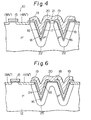
- Figure 6 shows the constitution of a memory cell used in a semiconductor memory device according to still another embodiment of the present invention.
- the end, on the transfer gate transistor side, of the insulation film 24 formed on the inside surface of the V-shaped groove 16 of the semiconductor substrate 12 does not extend on the top of the substrate 12 and is formed only along the inside surface portion of the V-shaped groove 16.
- the marginal portion between the end of the source region 14 and the verge of the groove as seen in the preceeding enbodiments is omitted on account of the production process explained later. This makes it possible to reduce the distance between the transfer gate transistor and the V-shaped groove 16 and, thus, to reduce the size of the memory cells.
- a P +-type diffusion layer 25 is formed under the groove 16, etc. to offer a large capacitance with a small occupied area. Further, in the memory cell of Fig. 6, no field oxide film is provided for isolating the capacitors of adjoining memory cells. This enables further reduction of the size of the memory cells.
- Other portions are the same as in the memory cells of Fig. 2 or Fig. 4 and are shown by the same reference numerals or characters.
- a nitride film (Si 3 N 4 ) 26 is formed on a region from the portion of the semiconductor substrate where the transfer gate transistor is to be formed to part of the region of the portion where the V-shaped groove is to be formed.
- Fig. 7B the same method is used to form the V-shaped groove 16.
- the nitride film 26 is used as a mask for the diffusion of boron, etc. by vapor growth deposition and the fomation of a P layer 25.
- vapor growth deposition is utilized for the growth of an oxide film on the grooves 16 and the center portion 27 between grooves. Portions other than this are covered by the nitride film. Since the nitride film does not pass oxygen, these portions are not oxidized. This is shown by Fig. 7C.
- Fig. 7D the nitride film 26 is removed. After this, the same processes as in Figs. 5E, 5F, and 5G are used for the formation of the memory cell of Fig. 6.
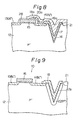
- Figure 8 illustrates a memory cell used in a semiconductor memory device as another embodiment of the present invention.
- a first conductive layer 18a, an insulation film 19a, and a second conductive layer 20a extend over a gate conductive layer 15 via an insulation layer 28.
- the other portions of Fig. 8 are the same as those of Fig. 2 and are designated by the same reference numerals. According to this embodiment, it is possible to further increase the capacitance of each memory cell and to increase the reliability of data storage.
- Figure 9 illustrates a memory cell used in a semiconductor memory device as another embodiment of the present invention.
- the memory cell of Fig. 9 is substantially the same as that of Fig. 4 except that the memory cell of Fig. 9 does not have the second conductive layer 20 shown in Fig. 4. Therefore, the capacitance for storing data is formed only by the first conductive layer 18 and the P + -type layer 22 formed under the groove portion 16 of the semiconductor substrate opposing each other via the insulation layer 17a.
- the first conductive layer 18 is electrically coupled to the source 14 of the transfer gate transistor 10 and is used for storing electric charges according to the memorized information. It should be noted that, in the aforementioned memory cell of Fig.
- the conductive layer 6 formed on the inside surface of the groove portion is not connected to the source 3 of the transfer gate transistor, but is connected to a power source or the ground. That is, in the memory cell of Fig. 1, the common electrode of the capacitor is the conductive layer 6, while, in the memory cell of Fig. 9, the common electrode of the capacitor is the P +- type layer 22 of the substrate 12.
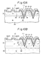
- FIGS 10A and 10B illustrate memory cells used in semiconductor memory devices as other embodiments of the present invention, respectively.
- a semiconductor substrate 30 has the N-type conductivity which is the same as that of the drain 13 and the source 14 of the transfer gate transistor 10.
- On the N-type substrate 30 is formed a P - -type semiconductor layer 31 having opposite conductivity type to that of the substrate.
- the P -type semiconductor layer 31 is formed by, for example, epitaxial growth or ion implantation, and has the thickness of, for example, 2 to 3 microns.
- the drain 13 and the source 14 are formed on the P -type semiconductor layer 31.
- the capacitor of the memory cell is formed on a V-shaped groove 16 formed from the surface of the semiconductor layer 31 toward the substrate 30, and has the same structure as that of the memory cell of Fig. 2.
- a reverse biased voltage is added between the P -type semiconductor layer 31 and the N-type substrate 30 .
- a voltage V cc is supplied, i.e., +5 V
- V ss is supplied, i.e., 0 V or V bb , i.e., -2 to -3 V.
- the depletion layer 33 is formed along the surface of the P -type semiconductor layer 31, i.e., under the area of the N + diffusion layer 14, and under the insulating film 17 on which the conductive layer 18 is arranged.
- the depletion layer 33 is also formed along the boundary P -type semiconductor layer 31 and the N-type substrate 30.
- the depletion region formed along the boundary of the P--type semiconductor layer 31 and the N-type substrate 30 be in contact with at least a part of the groove 16.
- Figure 11 illustrates a memory cell used in a semiconductor memory device as another embodiment of the present invention.
- the above-mentioned P -type semiconductor layer is not formed in the intermediate portion of the grooves of the mutually adjoining memory cells. Therefore, electrons generated by the alpha particles radiated into the intermediate portion are mostly absorbed by the N-type substrate 30, and the number of electrons flowing into the N +- type diffusion layer 14 is greatly decreased. Moreover, since the depletion layer is not formed in the intermediate portion, the capacitance between the first conductive layer 18 and the N-type substrate becomes great, thereby increasing the stability of data storage.
- the present invention provides a semiconductor memory device having memory cells with groove-type capacitors and transfer gate transistors, wherein the electrode of a groove-type capacitor connected to the source of a transfer gate transistor is formed on an insulation film attached to the inside surface of a groove formed in the substrate, eliminating the punchthrough phenomenon, etc. between the grooves of capacitors of adjoining memory cells and therefore enabling reduction of the distance between the grooves and a higher degree of integration. Further, it prevents the occurrence of leakage at groove portions due to stress induced by heat treatment, etc. in the fabrication processes and thus improves the reliability of the memory device. Moreover, the present invention provides a semiconductor memory device which can store data stably and reliably without being affected by the radiation of alpha particles.
Abstract
Description
- The present invention relates to a semiconductor memory device, more particularly, to a semiconductor memory device wherein memory cells are comprised by transistors and so-called groove-type capacitors.
- In general, in a dynamic-type semiconductor memory device, each memory cell is comprised by a single MOS transistor and a single capacitor. Such a memory cell enables improved integration of the circuit due to the low number of elements, used and, therefore, increased storage density. However, the capacitance of each memory cell preferably should be as large as possible since it is necessary to hold stored data stably for as long a period as possible, and large cell capacitance is also required for increasing the immunity against soft error caused by the radiation of alpha particles. Therefore, to further increase the degree of integration of a semiconductor memory device using such memory cells and, therefore, the storage density, it is necessary to use capacitors offering large capacities with small occupied areas as the capacitors of the memory cells.
- In a conventional dynamic-type semiconductor memory device, each memory cell is comprised by a transfer gate MOS transistor and a capacitor. The capacitor is a so-called groove-type capacitor and is comprised by providing a V-shaped or U-shaped groove on a semiconductor substrate, attaching a thin insulation film on the inside surface of the groove, and forming a polycrystalline silicon layer on the insulation film. The capacitor to store data is formed between an inversion layer which is formed along the groove and which is electrically coupled to the source of the transfer gate MOS transistor and the polycrystalline silicon layer, so that a large capacitance is realized in a small cell area.
- However, in the above-mentioned conventional memory device, when the distance between the capacitor grooves of adjoining memory cells is too small, the depletion layer formed under the grooves overflows the entire region between the grooves. Therefore, in this case, the punchthrough phenomenon easily occurs in this region and cells become electrically connected, thereby causing the stored information to be destroyed. Thus, in the conventional memory device, it is impossible to reduce the distance between the grooves of the adjacent memory cells and thus to increase the degree of integration of the device.
- In order to solve the aforementioned problems of the conventional memory device, the present invention adopts an idea of forming on a inside surface of a groove a capacitor electrode connected to the source of a transfer gate transistor and used to store electric charges according to the stored data, in a semiconductor memory device provided with memory cells each having a transfer gate transistor and a groove-type capacitor.
- It is an object of the present invention to enable reduction of the distance between the grooves of capacitors of adjoining memory cells so as to improve the degree of integration.
- It is another object of the present invention to prevent the occurrence of leakage between electrodes of capacitors by stress, etc. induced by heat treatment, etc. so sa to improve the reliability and yield of the semiconductor memory device.
- According to the present invention, there is provided a semiconductor memory device provided with memory cells each comprising: a transfer gate transistor having a drain, a source, and a gate formed on the channel region between the drain and source via a gate insulation film; and a capacitor having a conductive layer formed on an insulation film attached to the inside surface of a groove formed on a substrate, the conductive layer being electrically coupled to the source of the transfer gate transistor.
-
- Figure 1 is a cross-sectional view showing a memory cell in a conventional semiconductor memory device;
- Fig. 2 is a cross-sectional view showing a memory cell in a semiconductor memory device according to an embodiment of the present invention;
- Fig. 3A to Fig. 3E are views of the fabrication process for explaining the method of fabrication of the memory cell of Fig. 2;
- Fig. 4 is a cross-sectional view showing a memory cell used in a semiconductor memory device according to another embodiment of the present invention;
- Fig. 5A to Fig. 5G are views of the fabrication process for explaining the method of fabrication of the memory cell of Fig. 4;
- Fig. 6 is a cross-sectional view showing a memory cell used in a semiconductor memory device according to still another embodiment of the present invention;
- Fig. 7A to Fig. 7D are views of the fabrication process for explaining the method of fabrication of the memory cell of Fib. 6; and
- Figs. 8, 9, 10A, 10B, and 11 are cross-sectional views each showing a memory cell in a semiconductor memory device according to an embodiment of the present invention.
- Before describing the preferred embodiments, an explanation will be given of a conventional memory device.
- Figure 1 shows a construction of a memory cell used in a conventional dynamic type semiconductor memory device. The illustrated memory cell is comprised by a single transfer gate MOS transistor and a single capacitor for each bit. The MOS transistor is comprised, for example, with N+-
type diffusion layers type semiconductor substrate 1 as its drain and source and with apolycrystalline silicon layer 4 formed on a channel region between the N+-type diffusion layers type substrate 1, attaching a thin insulation film 5 on the inside surface of the groove, and forming apolycrystalline silicon layer 6 on the insulation film 5.Reference numeral 7 is a field oxide film for isolation from a capacitor of the adjoining memory cell. - In the memory cell of Fig. 1, one electrode plate of the capacitor is formed by an inversion layer at the surface portion of the V-shaped groove of the P -
type substrate 1 which can be generated by introduction of N-type impurity into the surface portion or application of a positive potential to theconductive layer 6. A capacitance is formed between this inversion layer and theconductive layer 6. Therefore, a capacitor electrode is formed along the V-shaped groove and, thus, it is possible to obtain a large capacitance with a small substrate surface area. - However, in the memory cell of Fig. 1, a
depletion layer 8 is formed in the range indicated by the dotted lines. When the distance between capacitor grooves of adjoining memory cells is small, this depletion layer overflows the entire region between grooves and thus the punchthrough phenomenon easily occurs in this region. When the punchthrough phenomenon occurs, the inversion layers formed along adjacent grooves are electrically connected to each other and the stored information is destroyed. Therefore, there is the disadvantage that it is not possible to reduce the distance between grooves and improve the degree of integration of the memory device too much. Further, in the memory cell of Fig. 1, there is the disadvantage that when stress is applied due to heat treatment, dislocation, etc. occurs in the crystals, leakage easily occurs in the groove portions, and information is destroyed. - According to the present invention, there is provided a semiconductor memory device which overcomes these problems.
- Below, a description will be given of an embodiment of the present invention in reference to the drawings. Figure 2 shows a cross-section of a memory cell used in a semiconductor memory device according to an embodiment of the present invention. The illustrated memory cell is provided with a transfer
gate MOS transistor 10 and a groove-type capacitor 11. TheMOS transistor 10 is comprised with N+-type diffusion layers type semiconductor substrate 12 as its drain and source and with a polycrystalline silicon orother layer 15 formed on a channel region between the N+-type diffusion layers insulation film 17 formed on the inside surface of, for example, a V-shaped groove 16, and is provided with a firstconductive layer 18 of polycrystalline silicon, etc. formed on theinsulation film 17 and a secondconductive layer 20 formed on theconductive layer 18 via aninsulation film 19 shown by the solid line. In other words, the capacitor ll is comprised by theinsulation film 19 for a capacitor dielectric sandwiched between the opposing first and secondconductive layers Reference numeral 21 is a field oxide film for isolation between the capacitors of adjoining memory cells. The secondconductive layer 20 should be connected to a constant potential terminal, e.g., a ground terminal or a power source terminal so as to function as a common capacitor electrode plate. - In the memory cell of Fig. 2, the gate of the
MOS transistor 10, i.e., theconductive layer 15, is, for example, connected to the word line, while the drain, i.e., the N+-type diffusion layer 13, is connected to the bit line. The source, i.e., the N+-type diffusion layer 14, is connected with the firstconductive layer 18 of the capacitor 11, while the secondconductive layer 20 of the capacitor 11 is connected to the power source, when the potential of the word line becomes at a high level, theMOS transistor 10 turns ON and the capacitor 11 is connected to the bit line for reading and writing of data, i.e., an operation is performed to change or discharge the capacitor 11. - In the memory cell of Fig. 2, the capacitor electrode plate, which is connected to the
source region 14 and must be electrically isolated from that of other cell, is formed by the first electrode of the capacitor which is completely isolated by the isolation film. Therefore, it is possible to prevent the occurrence of the punchthrough phenomenon between adjoining capacitors and to reduce the distance between the grooves of adjoining capacitors to improve the degree of integration. Further, since the firstconductive layer 18 of the capacitor is isolated from the p--type substrate 12 by theinsulation layer 17, even if leakage occurs at the groove portion due to stress induced by heat treatment, etc., this leakage will not result in leakage of the charge of theconductive layer 18, and therefore, there is no destruction of information and it is possible to improve the reliability of the semiconductor memory device. - Next, an explanation will be given of a method for manufacturing the memory cell of Fig. 2 in reference to Fig. 3A to Fig. 3E. First, on the
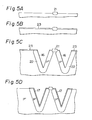
semiconductor substrate 12, as shown by Fig. 3A, is formed afield oxide film 21 which isolates the capacitors of adjoining memory cells, then reactive ion etching, etc. is performed for formation of, for example, the V-shaped groove. - Next, as shown by Fig. 3B, an
insulation film 17 is formed on the inside surface of thegroove 16. Thisinsulation film 17 is first attached to the substrate surface and the entire surface of thegroove 16, then photomasks, etc. are used for patterning so as to form theinsulation layer 17 as shown by Fig. 3B. - Next, as shown in Fig. 3C, a first layer
polycrystalline silicon layer 18 is formed on theinsulation film 17, etc. Thepolycrystalline silicon layer 18 is doped overall during or after growth with N-type impurities. - Further, as shown in Fig. 3D, the first layer
polycrystalline silicon layer 18 is subjected to CVD (chemical vapor deposition), etc. or the surface of the first layerpolycrystalline silicon layer 18 is oxidized so as to form theinsulation film 19 as shown by the solid lines in the figure. Then, a second layerpolycrystalline silicon layer 20 is formed on theinsulation film 19. - Next, as shown in Fig. 3E, a thin insulation film is formed on the substrate, then a third layer
polycrystalline silicon layer 15 for forming the gate electrode is formed. Subsequent to this, ion implantation, etc. is performed so as to form N+-type diffusion layers 13 and 14 for the drain and source using the gate electrode as a mask. Thus, the main fabricating processes for the memory cell are completed. - Figure 4 shows the construction of a memory cell used in a semiconductor memory device according to another embodiment of the present invention. The memory cell of the figure forms a P +-
type layer 22 under thegroove portion 16 of thesemiconductor substrate 12 so as to form a capacitance between the first layerpolycrystalline silicon layer 18 and said P layer, i.e., the substrate electrode, opposing each other across theinsulation layer 17 and uses this capacitance for data storage. By this construction, the capacitance of the capacitor of the memory cell can be made even larger and the data can be stored more reliably. The substrate in this case should be connected to a constant potential node, e.g., a ground terminal, so as to serve as a common capacitor electrode. - If there is no P layer, a depletion layer spreads directly under the
insulation film 17 and the capacitance between theconductive layer 18 and the substrate electrode becomes equivalent to a series connection of the capacitance of theinsulation film 17 and the capacitance of the depletion layer, whereupon a large capacitance cannot be obtained. - Another advantageous effect of the P layer is as follows: In Fig. 2, showing the first embodiment, there is no P layer. The problem here is that when the
insulation film 17 is thin and a high potential is stored in theconductive layer 18 as information, electric charges in the substrate surface invert and cause a conductive state of the substrate surface with thediffusion layer 14. When this happens, punchthrough occurs with the cells adjoining the inverted substrate surface portion of the groove and information can be easily destroyed. This problem can be improved by introduction of the P layer so as to make inversion more difficult. Other portions are the same as those of the memory cell of Fig. 2, so an explanation thereof is omitted. - Referring to Fig. 5A to Fig. 5G, an explanation will be made of the method of fabricating of the memory cell of Fig. 4. First, as shown in Fig. 5A, a thick
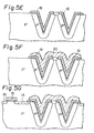
field oxide film 21 is formed to electrically isolate the capacitors of memory cells adjoining each other on a semiconductor substrate, then, as shown by Fig. 5B, the entire substrate is covered with anoxide film 23 of, for example, about 1,000 Angstroms. - Next, as shown in Fig. 5C, reactive ion etching or other methods are used to form the V-shaped
groove 16. This exposes the substrate at the portion of thegroove 16. At portions other than thegroove 16, the substrate is covered by theinsulation film 23 and thefield oxide film 21, therefore thisinsulation film 23 andfield oxide film 21 are used as masks for diffusion of boron or the like by vapor growth deposition or other methods on just the portion of thegroove 16 so as to form P+-type diffusion layers 22. - Next, as shown in Fig. 5D, an oxide film (SiO2, etc.) is formed at the portion of the
groove 16 as well. Then, the oxide film at portions other than necessary is removed for formation of theinsulation film 17. - After this, as shown by Figs. 5E, 5F, and 5G, the first layer
conductive layer 18,insulation film 19, second layerconductive layer 20, N+-type diffusion layers 13 and 14, third layerconductive layer 15, etc. are successively formed. These processes are the same as those of Figs. 3C, 3D, and 3E. - Figure 6 shows the constitution of a memory cell used in a semiconductor memory device according to still another embodiment of the present invention. In the memory cell of the figure, the end, on the transfer gate transistor side, of the
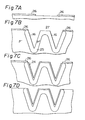
insulation film 24 formed on the inside surface of the V-shapedgroove 16 of thesemiconductor substrate 12 does not extend on the top of thesubstrate 12 and is formed only along the inside surface portion of the V-shapedgroove 16. The marginal portion between the end of thesource region 14 and the verge of the groove as seen in the preceeding enbodiments is omitted on account of the production process explained later. This makes it possible to reduce the distance between the transfer gate transistor and the V-shapedgroove 16 and, thus, to reduce the size of the memory cells. In the memory cell of Fig. 6, a P +-type diffusion layer 25 is formed under thegroove 16, etc. to offer a large capacitance with a small occupied area. Further, in the memory cell of Fig. 6, no field oxide film is provided for isolating the capacitors of adjoining memory cells. This enables further reduction of the size of the memory cells. Other portions are the same as in the memory cells of Fig. 2 or Fig. 4 and are shown by the same reference numerals or characters. - Next, referring to Figs. 7A to 7D, an explanation will be given of the method for fabricating the memory cell of Fig. 6. First, as shown in Fig. 7A, a nitride film (Si3N4) 26 is formed on a region from the portion of the semiconductor substrate where the transfer gate transistor is to be formed to part of the region of the portion where the V-shaped groove is to be formed.
- Next, as shown in Fig. 7B, the same method is used to form the V-shaped
groove 16. By this, the portion of thegroove 16 and theportion 27 between grooves of adjoining memory cells become free of thenitride film 26. Therefore thenitride film 26 is used as a mask for the diffusion of boron, etc. by vapor growth deposition and the fomation of aP layer 25. Next, vapor growth deposition is utilized for the growth of an oxide film on thegrooves 16 and thecenter portion 27 between grooves. Portions other than this are covered by the nitride film. Since the nitride film does not pass oxygen, these portions are not oxidized. This is shown by Fig. 7C. Next, as shown in Fig. 7D, thenitride film 26 is removed. After this, the same processes as in Figs. 5E, 5F, and 5G are used for the formation of the memory cell of Fig. 6. - Figure 8 illustrates a memory cell used in a semiconductor memory device as another embodiment of the present invention. In the memory cell of Fig. 8, a first conductive layer 18a, an
insulation film 19a, and a second conductive layer 20a extend over a gateconductive layer 15 via aninsulation layer 28. The other portions of Fig. 8 are the same as those of Fig. 2 and are designated by the same reference numerals. According to this embodiment, it is possible to further increase the capacitance of each memory cell and to increase the reliability of data storage. - Figure 9 illustrates a memory cell used in a semiconductor memory device as another embodiment of the present invention. The memory cell of Fig. 9 is substantially the same as that of Fig. 4 except that the memory cell of Fig. 9 does not have the second
conductive layer 20 shown in Fig. 4. Therefore, the capacitance for storing data is formed only by the firstconductive layer 18 and the P+-type layer 22 formed under thegroove portion 16 of the semiconductor substrate opposing each other via theinsulation layer 17a. The firstconductive layer 18 is electrically coupled to thesource 14 of thetransfer gate transistor 10 and is used for storing electric charges according to the memorized information. It should be noted that, in the aforementioned memory cell of Fig. 1 used in the conventional memory device, theconductive layer 6 formed on the inside surface of the groove portion is not connected to thesource 3 of the transfer gate transistor, but is connected to a power source or the ground. That is, in the memory cell of Fig. 1, the common electrode of the capacitor is theconductive layer 6, while, in the memory cell of Fig. 9, the common electrode of the capacitor is the P+-type layer 22 of thesubstrate 12. - Figures 10A and 10B illustrate memory cells used in semiconductor memory devices as other embodiments of the present invention, respectively. In each of the figures, a
semiconductor substrate 30 has the N-type conductivity which is the same as that of thedrain 13 and thesource 14 of thetransfer gate transistor 10. On the N-type substrate 30 is formed a P--type semiconductor layer 31 having opposite conductivity type to that of the substrate. The P -type semiconductor layer 31 is formed by, for example, epitaxial growth or ion implantation, and has the thickness of, for example, 2 to 3 microns. Thedrain 13 and thesource 14 are formed on the P -type semiconductor layer 31. The capacitor of the memory cell is formed on a V-shapedgroove 16 formed from the surface of thesemiconductor layer 31 toward thesubstrate 30, and has the same structure as that of the memory cell of Fig. 2. - Between the P -
type semiconductor layer 31 and the N-type substrate 30 is added a reverse biased voltage. For example, to the N-type substrate 30 a voltage Vcc is supplied, i.e., +5 V, and to the P--type semiconductor 31 a voltage Vss is supplied, i.e., 0 V or Vbb , i.e., -2 to -3 V. - The only difference between the memory cells of Figs. 10A and 10B is that the bottom of the
groove 16 reaches the N-type substrate 30 through the P -type layer 31 in Fig. 10A, but does not reach the N-type substrate 30 in Fig. 10B. - In the memory cell of Fig. l0A or 10B, when information "1", i.e., the high level potential V cc is stored in the capacitor 11, the potential of the first
conductive layer 18 and the N+-type diffusion layer 14 connected to the firstconductive layer 18 is the high level Vcc. The P -type semiconductor layer 31 and the N-type substrate 30 are kept in a reverse biased condition as mentioned before. Therefore, as shown by dotted lines, the depletion layer 33 is formed along the surface of the P -type semiconductor layer 31, i.e., under the area of the N+ diffusion layer 14, and under the insulatingfilm 17 on which theconductive layer 18 is arranged. The depletion layer 33 is also formed along the boundary P -type semiconductor layer 31 and the N-type substrate 30. - In such a condition, if alpha particles are radiated to the memory cell and electrons are generated in the depletion region under the N+-
type diffusion layer 14, the electrons flow into thediffusion layer 14. However, if alpha rays are radiated into the groove portion and electrons are generated in the depletion region under theinsulation film 16, the electrons move along the electric field of the depletion region and are gathered to the boundary surface of thegroove 16. A part of the electrons in the boundary surface of thegroove 16 flows into the N-type substrate 30 whose potential is high, e.g., Vcc , along the boundary surface. Therefore, although a part of the electrons in the boundary surface flows into the N+-type diffusion layer 14, the quantity of the electrons flowing into the N+-type diffusion layer 14 is much decreased, and the probability of the destruction of data stored in the memory cell is greatly decreased. - It should be noted that, in order to pass the electrons in the depletion region into the N-
type substrate 30, it is necessary that the depletion region formed along the boundary of the P--type semiconductor layer 31 and the N-type substrate 30 be in contact with at least a part of thegroove 16. - Figure 11 illustrates a memory cell used in a semiconductor memory device as another embodiment of the present invention. In the memory device of Fig. 11, the above-mentioned P -type semiconductor layer is not formed in the intermediate portion of the grooves of the mutually adjoining memory cells. Therefore, electrons generated by the alpha particles radiated into the intermediate portion are mostly absorbed by the N-
type substrate 30, and the number of electrons flowing into the N+-type diffusion layer 14 is greatly decreased. Moreover, since the depletion layer is not formed in the intermediate portion, the capacitance between the firstconductive layer 18 and the N-type substrate becomes great, thereby increasing the stability of data storage. - As explained above, the present invention provides a semiconductor memory device having memory cells with groove-type capacitors and transfer gate transistors, wherein the electrode of a groove-type capacitor connected to the source of a transfer gate transistor is formed on an insulation film attached to the inside surface of a groove formed in the substrate, eliminating the punchthrough phenomenon, etc. between the grooves of capacitors of adjoining memory cells and therefore enabling reduction of the distance between the grooves and a higher degree of integration. Further, it prevents the occurrence of leakage at groove portions due to stress induced by heat treatment, etc. in the fabrication processes and thus improves the reliability of the memory device. Moreover, the present invention provides a semiconductor memory device which can store data stably and reliably without being affected by the radiation of alpha particles.
Claims (12)
Applications Claiming Priority (2)
| Application Number | Priority Date | Filing Date | Title |
|---|---|---|---|
| JP233554/83 | 1983-12-13 | ||
| JP58233554A JPS60126861A (en) | 1983-12-13 | 1983-12-13 | Semiconductor memory device |
Publications (3)
| Publication Number | Publication Date |
|---|---|
| EP0145606A2 true EP0145606A2 (en) | 1985-06-19 |
| EP0145606A3 EP0145606A3 (en) | 1986-01-29 |
| EP0145606B1 EP0145606B1 (en) | 1991-03-06 |
Family
ID=16956879
Family Applications (1)
| Application Number | Title | Priority Date | Filing Date |
|---|---|---|---|
| EP84402560A Expired - Lifetime EP0145606B1 (en) | 1983-12-13 | 1984-12-12 | Semiconductor memory device |
Country Status (5)
| Country | Link |
|---|---|
| US (1) | US4646118A (en) |
| EP (1) | EP0145606B1 (en) |
| JP (1) | JPS60126861A (en) |
| KR (1) | KR910002030B1 (en) |
| DE (1) | DE3484232D1 (en) |
Cited By (9)
| Publication number | Priority date | Publication date | Assignee | Title |
|---|---|---|---|---|
| US4679300A (en) * | 1985-10-07 | 1987-07-14 | Thomson Components-Mostek Corp. | Method of making a trench capacitor and dram memory cell |
| GB2188776A (en) * | 1986-03-07 | 1987-10-07 | Canon Kk | Method of manufacturing semiconductor memory capacitor |
| US4791610A (en) * | 1985-05-24 | 1988-12-13 | Fujitsu Limited | Semiconductor memory device formed of a SOI-type transistor and a capacitor |
| GB2205993A (en) * | 1987-04-30 | 1988-12-21 | Samsung Semiconductor Tele | Method of manufacturing a trench capacitor |
| DE3832414A1 (en) * | 1987-11-28 | 1989-06-08 | Mitsubishi Electric Corp | SEMICONDUCTOR MEMORY DEVICE |
| GB2223879A (en) * | 1988-10-13 | 1990-04-18 | Crystal Semiconductor Corp | Compensated capacitors for switched capacitor input of an analog-to-digital converter |
| US5208597A (en) * | 1988-10-13 | 1993-05-04 | Crystal Semiconductor | Compensated capacitors for switched capacitor input of an analog-to-digital converter |
| EP0540163A2 (en) * | 1991-09-23 | 1993-05-05 | Xerox Corporation | Switched capacitor analog circuits |
| US5342792A (en) * | 1986-03-07 | 1994-08-30 | Canon Kabushiki Kaisha | Method of manufacturing semiconductor memory element |
Families Citing this family (17)
| Publication number | Priority date | Publication date | Assignee | Title |
|---|---|---|---|---|
| JPS6161441A (en) * | 1984-09-03 | 1986-03-29 | Toshiba Corp | Manufacture of semiconductor device |
| US4791463A (en) * | 1984-10-31 | 1988-12-13 | Texas Instruments Incorporated | Structure for contacting devices in three dimensional circuitry |
| JPH0650765B2 (en) * | 1985-08-28 | 1994-06-29 | 日本電気株式会社 | Method for manufacturing semiconductor device |
| JPS6239053A (en) * | 1985-08-14 | 1987-02-20 | Nec Corp | Semiconductor memory cell and manufacture thereof |
| US4896293A (en) * | 1988-06-09 | 1990-01-23 | Texas Instruments Incorporated | Dynamic ram cell with isolated trench capacitors |
| US5057887A (en) * | 1989-05-14 | 1991-10-15 | Texas Instruments Incorporated | High density dynamic ram cell |
| JPH0770618B2 (en) * | 1989-05-22 | 1995-07-31 | 三菱電機株式会社 | Semiconductor memory device and manufacturing method thereof |
| JP2551203B2 (en) * | 1990-06-05 | 1996-11-06 | 三菱電機株式会社 | Semiconductor device |
| KR970001894B1 (en) * | 1991-09-13 | 1997-02-18 | Nippon Electric Kk | Semiconductor memory device |
| KR0157912B1 (en) * | 1995-11-28 | 1998-12-15 | 문정환 | Capacitor electrode structure of semiconductor and method of manufacturing that |
| US5614431A (en) * | 1995-12-20 | 1997-03-25 | International Business Machines Corporation | Method of making buried strap trench cell yielding an extended transistor |
| US5793075A (en) * | 1996-07-30 | 1998-08-11 | International Business Machines Corporation | Deep trench cell capacitor with inverting counter electrode |
| JP3749776B2 (en) | 1997-02-28 | 2006-03-01 | 株式会社東芝 | Semiconductor device |
| US6222254B1 (en) * | 1997-03-31 | 2001-04-24 | Intel Corporation | Thermal conducting trench in a semiconductor structure and method for forming the same |
| US7067406B2 (en) * | 1997-03-31 | 2006-06-27 | Intel Corporation | Thermal conducting trench in a semiconductor structure and method for forming the same |
| US9431107B2 (en) | 2012-12-14 | 2016-08-30 | Taiwan Semiconductor Manufacturing Company, Ltd. | Memory devices and methods of manufacture thereof |
| KR102279921B1 (en) * | 2014-02-12 | 2021-07-22 | 삼성디스플레이 주식회사 | Organic light emitting display device and method of manufacturing the same |
Citations (5)
| Publication number | Priority date | Publication date | Assignee | Title |
|---|---|---|---|---|
| DE2441385A1 (en) * | 1974-08-29 | 1976-03-11 | Siemens Ag | Single transistor storage component - has a field-effect transistor and an mis capacitor on a doped SC substrate |
| EP0018764A1 (en) * | 1979-05-02 | 1980-11-12 | Fujitsu Limited | A semiconductor memory device in which soft errors due to alpha particles are prevented |
| JPS5643753A (en) * | 1979-09-18 | 1981-04-22 | Nippon Telegr & Teleph Corp <Ntt> | Semiconductor memory storage |
| JPS583260A (en) * | 1981-06-29 | 1983-01-10 | Fujitsu Ltd | Vertical type buried capacitor |
| EP0085988A2 (en) * | 1982-02-10 | 1983-08-17 | Hitachi, Ltd. | Semiconductor memory and method for fabricating the same |
Family Cites Families (8)
| Publication number | Priority date | Publication date | Assignee | Title |
|---|---|---|---|---|
| JPS538581A (en) * | 1976-07-12 | 1978-01-26 | Nec Corp | Semiconductor memory unit |
| JPS5394191A (en) * | 1977-01-28 | 1978-08-17 | Toshiba Corp | Semiconductor device |
| US4163243A (en) * | 1977-09-30 | 1979-07-31 | Hewlett-Packard Company | One-transistor memory cell with enhanced capacitance |
| JPS5524429A (en) * | 1978-08-09 | 1980-02-21 | Mitsubishi Electric Corp | Punch-through type constant-voltage diode and its manufacturing method |
| JPS5632757A (en) * | 1979-08-25 | 1981-04-02 | Semiconductor Res Found | Insulated gate type transistor and integrated circuit |
| US4466180A (en) * | 1981-06-25 | 1984-08-21 | Rockwell International Corporation | Method of manufacturing punch through voltage regulator diodes utilizing shaping and selective doping |
| JPS582360A (en) * | 1981-06-30 | 1983-01-07 | Toyota Central Res & Dev Lab Inc | Coating composition having resistance to filiform corrosion |
| US4507159A (en) * | 1981-10-07 | 1985-03-26 | Advanced Micro Devices, Inc. | Method of manufacturing high capacity semiconductor capacitance devices |
-
1983
- 1983-12-13 JP JP58233554A patent/JPS60126861A/en active Granted
-
1984
- 1984-12-12 EP EP84402560A patent/EP0145606B1/en not_active Expired - Lifetime
- 1984-12-12 DE DE8484402560T patent/DE3484232D1/en not_active Expired - Lifetime
- 1984-12-13 US US06/681,290 patent/US4646118A/en not_active Expired - Lifetime
- 1984-12-13 KR KR8407894A patent/KR910002030B1/en not_active IP Right Cessation
Patent Citations (5)
| Publication number | Priority date | Publication date | Assignee | Title |
|---|---|---|---|---|
| DE2441385A1 (en) * | 1974-08-29 | 1976-03-11 | Siemens Ag | Single transistor storage component - has a field-effect transistor and an mis capacitor on a doped SC substrate |
| EP0018764A1 (en) * | 1979-05-02 | 1980-11-12 | Fujitsu Limited | A semiconductor memory device in which soft errors due to alpha particles are prevented |
| JPS5643753A (en) * | 1979-09-18 | 1981-04-22 | Nippon Telegr & Teleph Corp <Ntt> | Semiconductor memory storage |
| JPS583260A (en) * | 1981-06-29 | 1983-01-10 | Fujitsu Ltd | Vertical type buried capacitor |
| EP0085988A2 (en) * | 1982-02-10 | 1983-08-17 | Hitachi, Ltd. | Semiconductor memory and method for fabricating the same |
Non-Patent Citations (3)
| Title |
|---|
| IBM TECHNICAL DISCLOSURE BULLETIN, vol. 22, no. 8a, January 1980, pages 3208-3209, Armonk, New York, US; B.J. MASTERS: "Reduction of alpha-induced soft errors in dynamic memories" * |
| PATENT ABSTRACTS OF JAPAN, vol. 5, no. 99 (E-63)[771], 21st June 1981; & JP-A-56 043 753 (NIPPON DENSHIN DENWA KOSHA) 22-04-1981 * |
| PATENT ABSTRACTS OF JAPAN, vol. 7, no. 72 (E-166)[1217], 25th March 1983; & JP-A-58 003 260 (FUJITSU K.K.) 10-01-1983 * |
Cited By (15)
| Publication number | Priority date | Publication date | Assignee | Title |
|---|---|---|---|---|
| US4791610A (en) * | 1985-05-24 | 1988-12-13 | Fujitsu Limited | Semiconductor memory device formed of a SOI-type transistor and a capacitor |
| US4679300A (en) * | 1985-10-07 | 1987-07-14 | Thomson Components-Mostek Corp. | Method of making a trench capacitor and dram memory cell |
| GB2188776A (en) * | 1986-03-07 | 1987-10-07 | Canon Kk | Method of manufacturing semiconductor memory capacitor |
| GB2188776B (en) * | 1986-03-07 | 1989-11-01 | Canon Kk | Method of manufacturing semiconductor memory element |
| US5342792A (en) * | 1986-03-07 | 1994-08-30 | Canon Kabushiki Kaisha | Method of manufacturing semiconductor memory element |
| GB2205993A (en) * | 1987-04-30 | 1988-12-21 | Samsung Semiconductor Tele | Method of manufacturing a trench capacitor |
| US4970580A (en) * | 1987-11-28 | 1990-11-13 | Mitsubishi Denki Kabushiki Kaisha | Semiconductor memory device having protruding cell configuration |
| DE3832414A1 (en) * | 1987-11-28 | 1989-06-08 | Mitsubishi Electric Corp | SEMICONDUCTOR MEMORY DEVICE |
| GB2223879A (en) * | 1988-10-13 | 1990-04-18 | Crystal Semiconductor Corp | Compensated capacitors for switched capacitor input of an analog-to-digital converter |
| GB2223879B (en) * | 1988-10-13 | 1993-03-17 | Crystal Semiconductor Corp | Delta-sigma modulator with switch capacitor for input to an analog-to-digital converter |
| US5208597A (en) * | 1988-10-13 | 1993-05-04 | Crystal Semiconductor | Compensated capacitors for switched capacitor input of an analog-to-digital converter |
| DE3933552A1 (en) * | 1988-10-13 | 1990-04-19 | Crystal Semiconductor Corp | COMPENSATED CAPACITOR FOR THE INPUT OF ANALOG / DIGITAL CONVERTER WITH SWITCHED CAPACITOR |
| EP0540163A2 (en) * | 1991-09-23 | 1993-05-05 | Xerox Corporation | Switched capacitor analog circuits |
| EP0540163A3 (en) * | 1991-09-23 | 1994-06-15 | Xerox Corp | Switched capacitor analog circuits |
| US5589847A (en) * | 1991-09-23 | 1996-12-31 | Xerox Corporation | Switched capacitor analog circuits using polysilicon thin film technology |
Also Published As
| Publication number | Publication date |
|---|---|
| JPH0562468B2 (en) | 1993-09-08 |
| US4646118A (en) | 1987-02-24 |
| KR910002030B1 (en) | 1991-03-30 |
| DE3484232D1 (en) | 1991-04-11 |
| KR850004875A (en) | 1985-07-27 |
| JPS60126861A (en) | 1985-07-06 |
| EP0145606B1 (en) | 1991-03-06 |
| EP0145606A3 (en) | 1986-01-29 |
Similar Documents
| Publication | Publication Date | Title |
|---|---|---|
| US4646118A (en) | Semiconductor memory device | |
| EP0175378B1 (en) | Dynamic random access memory (dram) | |
| KR900000207B1 (en) | Semiconductor memory device with trench surrounding each memory cell | |
| US4794563A (en) | Semiconductor memory device having a high capacitance storage capacitor | |
| US4798794A (en) | Method for manufacturing dynamic memory cell | |
| GB1591429A (en) | Fabrication methods for the high capacity ram cell | |
| JPH06151772A (en) | Sram provided with double vertical channel and its manufacture | |
| US5041887A (en) | Semiconductor memory device | |
| JP3272979B2 (en) | Semiconductor device | |
| EP0098165B1 (en) | Semiconductor memory device | |
| GB2233154A (en) | Manufacturing a DRAM cell semi-conductor device | |
| JPH0715949B2 (en) | DRAM cell and manufacturing method thereof | |
| JPH0640573B2 (en) | Semiconductor integrated circuit device | |
| JPS59191374A (en) | Semiconductor integrated circuit device | |
| KR950012744B1 (en) | Method of producing semiconductor memory device | |
| JPH0642534B2 (en) | Method of forming a contact on a wall extending to a substrate | |
| JPH08139206A (en) | Semiconductor device and manufacture of the same | |
| JPH08274189A (en) | Semiconductor device and its manufacture | |
| JP2550119B2 (en) | Semiconductor memory device | |
| JPH077823B2 (en) | Semiconductor integrated circuit device | |
| JP2554332B2 (en) | 1-transistor type dynamic memory cell | |
| JPS61199657A (en) | Semiconductor memory | |
| JPS61140171A (en) | Semiconductor memory device | |
| JPH0621387A (en) | Semiconductor memory and manufacture thereof | |
| KR900005355B1 (en) | Semiconductor memory device and manufacturing method thereof |
Legal Events
| Date | Code | Title | Description |
|---|---|---|---|
| PUAI | Public reference made under article 153(3) epc to a published international application that has entered the european phase |
Free format text: ORIGINAL CODE: 0009012 |
|
| AK | Designated contracting states |
Designated state(s): DE FR GB |
|
| PUAL | Search report despatched |
Free format text: ORIGINAL CODE: 0009013 |
|
| AK | Designated contracting states |
Designated state(s): DE FR GB |
|
| 17P | Request for examination filed |
Effective date: 19860719 |
|
| 17Q | First examination report despatched |
Effective date: 19871204 |
|
| GRAA | (expected) grant |
Free format text: ORIGINAL CODE: 0009210 |
|
| AK | Designated contracting states |
Kind code of ref document: B1 Designated state(s): DE FR GB |
|
| REF | Corresponds to: |
Ref document number: 3484232 Country of ref document: DE Date of ref document: 19910411 |
|
| ET | Fr: translation filed | ||
| PLBE | No opposition filed within time limit |
Free format text: ORIGINAL CODE: 0009261 |
|
| STAA | Information on the status of an ep patent application or granted ep patent |
Free format text: STATUS: NO OPPOSITION FILED WITHIN TIME LIMIT |
|
| 26N | No opposition filed | ||
| REG | Reference to a national code |
Ref country code: GB Ref legal event code: IF02 |
|
| PGFP | Annual fee paid to national office [announced via postgrant information from national office to epo] |
Ref country code: GB Payment date: 20031210 Year of fee payment: 20 Ref country code: FR Payment date: 20031210 Year of fee payment: 20 |
|
| PGFP | Annual fee paid to national office [announced via postgrant information from national office to epo] |
Ref country code: DE Payment date: 20031229 Year of fee payment: 20 |
|
| PG25 | Lapsed in a contracting state [announced via postgrant information from national office to epo] |
Ref country code: GB Free format text: LAPSE BECAUSE OF EXPIRATION OF PROTECTION Effective date: 20041211 |
|
| REG | Reference to a national code |
Ref country code: GB Ref legal event code: PE20 |