EP0142400A1 - Housing for an electronic component, especially for telephone protection - Google Patents
Housing for an electronic component, especially for telephone protection Download PDFInfo
- Publication number
- EP0142400A1 EP0142400A1 EP84401912A EP84401912A EP0142400A1 EP 0142400 A1 EP0142400 A1 EP 0142400A1 EP 84401912 A EP84401912 A EP 84401912A EP 84401912 A EP84401912 A EP 84401912A EP 0142400 A1 EP0142400 A1 EP 0142400A1
- Authority
- EP
- European Patent Office
- Prior art keywords
- housing
- contact
- contacts
- electronic component
- base
- Prior art date
- Legal status (The legal status is an assumption and is not a legal conclusion. Google has not performed a legal analysis and makes no representation as to the accuracy of the status listed.)
- Granted
Links
Images

Classifications
-
- H—ELECTRICITY
- H05—ELECTRIC TECHNIQUES NOT OTHERWISE PROVIDED FOR
- H05K—PRINTED CIRCUITS; CASINGS OR CONSTRUCTIONAL DETAILS OF ELECTRIC APPARATUS; MANUFACTURE OF ASSEMBLAGES OF ELECTRICAL COMPONENTS
- H05K7/00—Constructional details common to different types of electric apparatus
- H05K7/20—Modifications to facilitate cooling, ventilating, or heating
- H05K7/2039—Modifications to facilitate cooling, ventilating, or heating characterised by the heat transfer by conduction from the heat generating element to a dissipating body
- H05K7/20436—Inner thermal coupling elements in heat dissipating housings, e.g. protrusions or depressions integrally formed in the housing
- H05K7/2049—Pressing means used to urge contact, e.g. springs
-
- H—ELECTRICITY
- H01—ELECTRIC ELEMENTS
- H01C—RESISTORS
- H01C1/00—Details
- H01C1/08—Cooling, heating or ventilating arrangements
- H01C1/084—Cooling, heating or ventilating arrangements using self-cooling, e.g. fins, heat sinks
-
- H—ELECTRICITY
- H01—ELECTRIC ELEMENTS
- H01L—SEMICONDUCTOR DEVICES NOT COVERED BY CLASS H10
- H01L2924/00—Indexing scheme for arrangements or methods for connecting or disconnecting semiconductor or solid-state bodies as covered by H01L24/00
- H01L2924/0001—Technical content checked by a classifier
- H01L2924/0002—Not covered by any one of groups H01L24/00, H01L24/00 and H01L2224/00
Definitions
- the present invention relates to a housing for an electronic component comprising two opposite planar faces coated with electrodes, said housing comprising a cover and a base crossed by at least first and second electrical contacts, the end of said contacts located in the housing being intended to be connected respectively to an electrode of the component.
- Telephone lines are the site of intense electrical disturbances due to atmospheric discharges as well as direct or induced galvanic connections with an electrical energy distribution line. It therefore proved necessary to protect them both against overvoltages and overcurrents which could lead to the destruction of the subscriber's central office or telephone handset.
- French patent 2,494,925 describes a component for telephone protection essentially consisting of a resistance with a positive temperature coefficient and a thermally coupled varistor. Besides the fact that such a component has a large parasitic capacity due to the production by two adjoining discs, no solution is given in this patent as to the connection of the elements to one another, their arrangement in a housing, in particular for obtain a component which inside its casing has low bulk characteristics, taking into account the constraints imposed by the manufacturers of telephone equipment.
- the housing according to the invention makes it possible to solve the various problems posed above.
- said electrical contact has one end external to the housing ensuring thermal dissipation by convection of calories by the component, the other part of the electrical contacts ensuring thermal conduction of said calories to said lower end .
- the two contacts arranged vertically, pass through the base substantially at 90 ° relative to each other, the first contact intended for contact with the lower electrode of the component comprising an H-shaped part, the two arms lower parts of the H constituting the connection tabs of the contact, said first contact further comprising in its middle a substantially horizontal part coming to bear on the bottom of the base of the housing, while the second contact intended for contact with the electrode of the component is an elastic contact provided with several fingers.
- the bottom of the base has an opening allowing the dissipation of calories by the reverse side of the horizontal part of the first contact, said base being able to be made of a material the softening temperature of which is lower than the maximum operating temperature of the component.
- the shape of this horizontal part of the second contact corresponds to the housing produced in the base and allows said contact to be held in a horizontal plane.
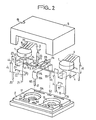
- Figure 1 an exploded view of a first embodiment of a housing according to the invention.
- This box comprises a base 8, a cover 9 and four electrical contacts 4 and 5, 6 and 7.
- the contacts 4 and 5 are intended for the connection of component 1 in the characteristic is to have two opposite planar faces provided with electrodes (not shown in the figure).
- this component 1 has the shape of a disc.
- the first contact 4 comprises a vertical H-shaped part and a horizontal part connected to the previous one between the two upper arms of the H. This contact has the particularity of being cut from a single piece and then folded at 90 °.
- the vertical part comprises, on its lower portion, the two lower arms of the H, 20 and 21 intended for the electrical connection on the printed circuit.
- a substantially rectangular contact body 70 comprising an elastic cutout 22 intended to maintain contact in a vertical plane after passing through the opening 34 of the base 8.
- the upper part thereof is located at a height D 3 from the base of the two lower arms of the H, this height D 3 determining the heat dissipation surface outside the housing of said contact 4.
- the two upper arms 23 and 24 of the vertical H-shaped part have two edges on their outer portions 45 and 46 abutting against the base 8.
- the horizontal part of the contact 4 is connected to the vertical part by the portion 25 of width and height corresponding exactly to the space 31 located between the two branches 23 and 24. It extended by a part 26 coming into electrical and thermal contact with the lower electrode of the component 1.
- This part 26 is externally limited by the portions 27, 28, 29 and 30 delimiting a diameter substantially equal to that of the internal groove 17 of the 'base 8, this in order to limit the horizontal displacement of the contact once it is fixed in the base 8.
- the second contact 5 whose lower part is identical to the lower part of the H-shaped vertical part of the first contact, so it has two connection tabs 71, 72, a body 73 intended for heat dissipation outside the base 8, an identical elastic holding device 74 at 22, so q eu on its upper part two flanges 47 (only one is shown in the figure) coming to bear on the base 8 after insertion of the contact 5 in the slot 37 of said base 8.
- the upper part of this second contact 5 comprises a first rectangular fold 75 substantially at 90 ° to the body of the contact 5, said rectangular portion extending by a plurality of elastic fingers 16 (four fingers are shown in the figure). These fingers are inclined in the example shown here substantially at approximately 30 ° relative to the horizontal. Each elastic finger is independent of the neighboring finger and its inclination and the length of each of the fingers is such that in the absence of component 1 intended to be electrically and thermally connected between the two contacts 4 and 5, there is no electrical contact between the first contact 4 and the second contact 5. This is a characteristic of the invention, allowing in the event of spraying due to an overvoltage or overcurrent of the component 1 to allow the assembly to behave like a switch open.
- the component housing according to the invention also comprises in the present case (but this is not essential, only the first and second contacts being) a third and a fourth contacts respectively 6 and 7 of identical shape.
- These contacts have a shape substantially identical to the vertical part of the first contact 4, namely two connection tabs 40, 41, 42, 43, a body 76, 77 whose lower part of height D 3 allows heat dissipation to outside the housing, and comprising an elastic fixing means 39, 44, making it possible to maintain the contact in a vertical position, after passage of the latter in the corresponding slot 36, 35 of the base 8.
- the upper part of these contacts comprises shoulders 50, 51, 48, 49, said shoulders also abutting against the walls of the base adjacent to the slots 36 and 35.
- These elements 2 and 3 can be either semi elements conductors (of the diode, thyristor, etc.), or passive elements such as varistors, resistors, etc.
- the height contact portion D 3 which has a heat dissipation function for the calories generated by the component 1 also has a second washing foot function facilitating the washing of the printed circuit after soldering the housing with these components on said circuit.
- the housing according to the invention allows thermal coupling between the components such as 1 and the components such as 2 and 3, taking into account the fact that these are always arranged substantially at the same distance from one of the 'other.
- a washer of thermal insulation such as an asbestos sheet, for example
- the contact elements 4, 5, 6, 7 will be made of metals such as beryllium bronze, stainless steel, etc. so as to ensure good electrical conductivity at the same time as elastic power.
- they are chosen to be thin (preferably from 1 to 4/10 mm, so as not to exhibit significant thermal inertia, which could slow the switching times of the circuit using them.
- the width of these contacts (substantially identical to the width of the slots such as 35, 36, 37, 34) will be large so that said contacts have large surfaces for electrical contact with the various components and to ensure good heat dissipation of the calories generated by the component 1, in particular in their parts of height D 1 , D 2 and D3.
- connection tabs 20 and 21 makes it possible on the one hand to strengthen the quality of fixing of the printed circuit and on the other hand to reduce the current density in the event of overload.
- the lower contact 4, in particular in its horizontal part 26, can be made of metal of the type known under the name "expanded metal", making it possible to increase the number of contact points due to the relief of it.
- a mark 19 placed on the cover 9 of the housing allows the external location of said housing in the case of automatic insertion using an adequate machine.
- Figure 2 shows a second embodiment of a housing according to the invention, housing in which are arranged two sets of contacts for component in the form of a disc such as a resistor with positive temperature coefficient PTC.
- the base 8 and the housing 9 are here of rectangular shape taking into account the presence of two sets of first and second contacts 4 and 5, arranged side by side.
- the contacts 4 and 5 of each assembly are identical in all respects to those described in the previous figure, as are the cells 17 located in the base 8, said cells 17 having, again, a keyhole-like shape as in the previous figure, with the opening 32 opening onto the underside of the base.
- a third contact 106 has been arranged with a shape different from that of the third and fourth contacts of the previous figure.
- the contact 106 simply comprises two connection tabs 112, 113, interconnected inside the housing by a flat portion 114 on which are arranged two arms 115 and 116 substantially perpendicular and upward. These two arms are intended for the connection of components such as 2 and 3 as envisaged in the description of FIG. 1.
- this contact 106 is not necessary if one wishes to use only one or two disc type components with electrodes.
Abstract
Description
La présente invention concerne un boîtier pour composant électronique comportant deux faces planes opposées revêtues d'électrodes, ledit boîtier comportant un capot et une embase traversés par au moins un premier et un deuxième contacts électriques, l'extrémité desdits contacts situées dans le boîtier étant destinée à être reliée respectivement à une électrode du composant.The present invention relates to a housing for an electronic component comprising two opposite planar faces coated with electrodes, said housing comprising a cover and a base crossed by at least first and second electrical contacts, the end of said contacts located in the housing being intended to be connected respectively to an electrode of the component.
Les lignes téléphoniques sont le siège de perturbations électriques intenses dues aux décharges atmosphériques ainsi qu'aux liaisons galvaniques directes ou induites avec une ligne de distribution d'énergie électrique. Il s'est donc avéré nécessaire de les protéger à la fois contre les surtensions et les surintensités pouvant entraîner la destruction du central ou du combiné téléphonique de l'abonné.Telephone lines are the site of intense electrical disturbances due to atmospheric discharges as well as direct or induced galvanic connections with an electrical energy distribution line. It therefore proved necessary to protect them both against overvoltages and overcurrents which could lead to the destruction of the subscriber's central office or telephone handset.
La façon la plus habituelle de réaliser le cablage des circuits de protection téléphonique est de faire appel à des composants discrets connectés par soudure sur la carte imprimée des circuits à protéger. Cette manière de faire présente cependant un certain nombre d'inconvénients :
- - le couplage thermique entre les différents composants qui permet, dans bien des cas, ainsi qu'on le verra par la suite, d'améliorer le fonctionnement de ces circuits, est très difficile à réaliser sur cette carte imprimée,
- - les composants discrets utilisés doivent posséder des fils de connexion, ce qui n'est pas le cas d'un certain nombre de composants tels que les résistances à coefficient de température très souvent utilisées dans ces circuits. Ce type de résistance est généralement réalisée sous forme d'un disque avec des métallisations en aluminium sur les deux faces circulaires opposées. La solution serait alors de souder directement un tel composant sur le circuit mais ceci nécessite l'utilisation de soudure à bas point de fusion pour ne pas endommager celui-ci. Par conséquent, on limite alors l'utilisation des résistances à coefficient de température fonctionnant à basse température.
- - the thermal coupling between the different components which, in many cases, as will be seen later, to improve the operation of these circuits, is very difficult to achieve on this circuit board,
- - the discrete components used must have connection wires, which is not the case for a certain number of components such as the resistors with temperature coefficient very often used in these circuits. This type of resistance is generally produced in the form of a disc with aluminum metallizations on the two opposite circular faces. The solution would then be to directly solder such a component on the circuit but this requires the use of low-melting solder to avoid damaging it. Consequently, the use of resistors with a temperature coefficient operating at low temperature is then limited.
Le brevet français 2 494 925 décrit un composant pour la protection téléphonique constitué essentiellement d'une résistance à coefficient de température positif et d'une varistance couplée thermiquement. Outre le fait qu'un tel composant présente une capacité parasite importante du fait de la réalisation par deux disques accolés, aucune solution n'est donnée dans ce brevet quant à la connexion des éléments entre eux, leur disposition dans un boîtier, en particulier pour obtenir un composant qui à l'intérieur de son boîtier possède de faibles caractéristiques d'encombrement, compte tenu des contraintes imposées par les constructeurs de matériel téléphonique.French patent 2,494,925 describes a component for telephone protection essentially consisting of a resistance with a positive temperature coefficient and a thermally coupled varistor. Besides the fact that such a component has a large parasitic capacity due to the production by two adjoining discs, no solution is given in this patent as to the connection of the elements to one another, their arrangement in a housing, in particular for obtain a component which inside its casing has low bulk characteristics, taking into account the constraints imposed by the manufacturers of telephone equipment.
Le boîtier selon l'invention permet de résoudre les différents problèmes posés ci-dessus. Dans ce but, il est caractérisé en ce que ledit contact électrique comporte une extrémité extérieure au boîtier assurant la dissipation thermique par convection des calories par le composant, l'autre partie des contacts électriques assurant la conduction thermique desdites calories jusqu'à ladite extrémité inférieure.The housing according to the invention makes it possible to solve the various problems posed above. For this purpose, it is characterized in that said electrical contact has one end external to the housing ensuring thermal dissipation by convection of calories by the component, the other part of the electrical contacts ensuring thermal conduction of said calories to said lower end .
De préférence, les deux contacts, disposées verticalement, traversent l'embase sensiblement à 90° l'un par rapport à l'autre, le premier contact destiné au contact avec l'électrode inférieure du composant comportant une partie en H, les deux bras inférieurs du H constituant les pattes de connexion du contact, ledit premier contact comportant en outre en son milieu une partie sensiblement horizontale venant s'appuyer sur le fond de l'embase du boîtier, tandis que le second contact destiné au contact avec l'électrode supérieure du composant est un contact élastique pourvu de plusieurs doigts.Preferably, the two contacts, arranged vertically, pass through the base substantially at 90 ° relative to each other, the first contact intended for contact with the lower electrode of the component comprising an H-shaped part, the two arms lower parts of the H constituting the connection tabs of the contact, said first contact further comprising in its middle a substantially horizontal part coming to bear on the bottom of the base of the housing, while the second contact intended for contact with the electrode of the component is an elastic contact provided with several fingers.
Selon un mode préférentiel de réalisation, le fond de l'embase posséde une ouverture permettant la dissipation des calories par le verso de la partie horizontale du premier contact, ladite embase pouvant être en matériau dont la température de ramollissement est inférieure à la température de fonctionnement maximal du composant. La forme de cette partie horizontale du second contact, correspond au logement réalisé dans l'embase et permet le maintien dans un plan horizontal dudit contact.According to a preferred embodiment, the bottom of the base has an opening allowing the dissipation of calories by the reverse side of the horizontal part of the first contact, said base being able to be made of a material the softening temperature of which is lower than the maximum operating temperature of the component. The shape of this horizontal part of the second contact corresponds to the housing produced in the base and allows said contact to be held in a horizontal plane.
L'invention sera mieux comprise à l'aide des exemples de réalisation suivants, donnés à titre non limitatif, conjointement avec les figures qui représentent :
- - la figure 1, un premier exemple de réalisation d'un boîtier selon l'invention comportant un élément sous forme de disque,
- - la figure 2, un second exemple de réalisation d'un boîtier selon l'invention comportant deux composants sous forme de disque.
- FIG. 1, a first embodiment of a housing according to the invention comprising an element in the form of a disc,
- - Figure 2, a second embodiment of a housing according to the invention comprising two components in the form of disc.
Sur la figure 1, est représentée une vue éclatée d'un premier mode de réalisation d'un boîtier selon l'invention. Ce boîtier comporte une embase 8, un capot 9 et quatre contacts électriques 4 et 5, 6 et 7. Les contacts 4 et 5 sont destinés à la connexion du composant 1 dans la caractéristique est de posséder deux faces planes opposées munies d'électrodes (non représentées sur la figure). Sur cette figure, ce composant 1 a la forme d'un disque. Le premier contact 4 comporte une partie verticale en forme de H et une partie horizontale raccordée à la précédente entre les deux bras supérieurs du H. Ce contact présente la particularité d'être découpée à partir d'une seule pièce puis pliée à 90°. La partie verticale comporte, sur sa portion inférieure, les deux bras inférieurs du H, 20 et 21 destinés à la connexion électrique sur circuit imprimé. Il se prolonge par un corps de contact 70 sensiblement rectangulaire, comportant une découpe élastique 22 destinée au maintien du contact dans un plan vertical après passage dans l'ouverture 34 de l'embase 8. La partie supérieure de celle-ci est située à une hauteur D3 à partir de la base des deux bras inférieurs du H, cette hauteur D3 déterminant la surface de dissipation thermique à l'extérieur du boîtier dudit contact 4. Les deux bras supérieurs 23 et 24 de la partie verticale en forme de H comportent sur leurs portions extérieures deux rebords 45 et 46 venant en butée contre l'embase 8. La partie horizontale du contact 4 est reliée à la partie verticale par la portion 25 de largeur et hauteur correspondant exactement à l'espace 31 situé entre les deux branches 23 et 24. Il se prolonge par une partie 26 venant en contact électrique et thermique avec l'électrode inférieure du composant 1. Cette partie 26 est limitée extérieurement par les portions 27, 28, 29 et 30 délimitant un diamètre sensiblement égal à celui de la rainure interne 17 de l'embase 8, ceci afin de limiter le déplacement horizontal du contact une fois celui-ci fixé dans l'embase 8. Disposé à 90" par rapport au premier contact 4, se trouve le second contact 5 dont la partie inférieure est identique à la partie inférieure de la partie verticale en forme de H du premier contact. Il comporte donc deux pattes de connexion 71, 72, un corps 73 destiné à la dissipation thermique à l'extérieur de l'embase 8, un dispositif de maintien élastique 74 identique à 22, ainsi que sur sa partie supérieure deux rebords 47 (un seul est représenté sur la figure) venant s'appuyer sur l'embase 8 après insertion du contact 5 dans la fente 37 de ladite embase 8. La partie supérieure de ce second contact 5 comporte un premier pli rectangulaire 75 sensiblement à 90° du corps du contact 5, ladite partie rectangulaire se prolongeant par une pluralité de doigts élastiques 16 (quatre doigts- sont représentés sur la figure). Ces doigts sont inclinés dans l'exemple représenté ici sensiblement à 30° environ par rapport à l'horizontal. Chaque doigt élastique est indépendant du doigt voisin et son inclinaison et la longueur de chacun des doigts est telle qu'en l'absence du composant 1 destiné à être connecté électriquement et thermiquement entre les deux contacts 4 et 5, il n'existe pas de contact électrique entre le premier contact 4 et le second contact 5. Ceci est une caractéristique de réalisation de l'invention, permettant en cas de pulvérisation due à une surtension ou surintensité du composant 1 de permettre à l'ensemble de se comporter comme un interrupteur ouvert.In Figure 1 is shown an exploded view of a first embodiment of a housing according to the invention. This box comprises a
Le boîtier pour composant selon l'invention comporte également dans le cas présent (mais ceci n'est pas indispensable, seul le premier et le second contacts l'étant) un troisième et un quatrième contacts respectivement 6 et 7 de forme identique. Ces contacts possèdent une forme sensiblement identique à la partie verticale du premier contact 4, à savoir deux pattes de connexion 40, 41, 42, 43, un corps 76, 77 dont la partie inférieure de hauteur D3 permet la dissipation thermique à l'extérieur du boîtier, et comportant un moyen de fixation élastique 39, 44, permettant de maintenir le contact en position verticale, après passage de celui-ci dans la fente correspondante 36, 35 de l'embase 8. La partie supérieure de ces contacts comporte des épaulements 50, 51, 48, 49, lesdits épaulements venant également en butée contre les parois de l'embase adjacentes aux fentes 36 et 35. La partie supérieure de ces contacts 6 et 7 prend une forme quelconque, permettant le raccordement éventuel de composants tels que 2 et 3 qui comportent des pattes de connexion externes 78, 79, 80, 81 reliant respectivement dans le cas présent le premier contact 4 au contact 6 et ce dernier au contact 7. Ces éléments 2 et 3 peuvent être soit des éléments semiconducteurs (du type diode, du thyristor, etc...), ou des éléments passifs tels que varistances, résistances, etc...The component housing according to the invention also comprises in the present case (but this is not essential, only the first and second contacts being) a third and a fourth contacts respectively 6 and 7 of identical shape. These contacts have a shape substantially identical to the vertical part of the first contact 4, namely two
Il est à noter également que la portion de contacts de hauteur D3 qui a une fonction de dissipation thermique des calories engendrées par le composant 1 a également une seconde fonction de pied de lavage facilitant le lavage du circuit imprimé après soudure du boîtier avec ces composants sur ledit circuit. On notera également que le boîtier selon l'invention permet un couplage thermique entre les composants tels que 1 et les composants tels que 2 et 3, compte tenu du fait que ceux-ci sont toujours disposés sensiblement à la même distance l'un de l'autre. Inversement, on peut prévoir une rondelle d'isolant thermique telle qu'une feuille d'amiante, par ) exemple, entre le composant 1 et les composants 2 et 3.It should also be noted that the height contact portion D 3 which has a heat dissipation function for the calories generated by the
Les éléments de contact 4, 5, 6, 7 seront en métaux tels que le bronze béryllium, l'inox, etc... de manière à assurer une bonne conductivité électique en même temps qu'un pouvoir élastique. Dans ce but, ils sont choisis d'épaisseur faible (de préférence de 1 à 4/10 mm, de manière à ne pas présenter d'inertie thermique importante, ce qui pourrait ralentir les temps de commutation du circuit les utilisant. Par ailleurs, la largeur de ces contacts (sensiblement identique à la largeur des fentes tels que 35, 36, 37, 34) sera importante de manière à ce que lesdits contacts présentent de larges surfaces pour le contact électrique avec les différents composants et pour assurer une bonne dissipation thermique des calories engendrées par le composant 1, en particulier dans leurs parties de hauteur D1, D2 et D3. Cette dissipation thermique par les parties de contact de hauteur D3 en particulier, hors des boîtiers, permettent d'abaisser la température desdits contacts au niveau des pattes de connexion telles que 20, 21, 71, 72, etc... De cette manière, le composant sous forme de disque 1 peut ainsi fonctionner à une température élevée voisine de 200° sans risque de voir lesdites pattes de connexion se désouder du circuit imprimé d'utilisation, même en utilisant une soudure étain-plomb à point de fusion relativement bas.The contact elements 4, 5, 6, 7 will be made of metals such as beryllium bronze, stainless steel, etc. so as to ensure good electrical conductivity at the same time as elastic power. For this purpose, they are chosen to be thin (preferably from 1 to 4/10 mm, so as not to exhibit significant thermal inertia, which could slow the switching times of the circuit using them. Furthermore, the width of these contacts (substantially identical to the width of the slots such as 35, 36, 37, 34) will be large so that said contacts have large surfaces for electrical contact with the various components and to ensure good heat dissipation of the calories generated by the
La présence de deux pattes de connexion 20 et 21 permet d'une part de renforcer la qualité de fixation de circuit imprimé et d'autre part de réduire la densité de courant en cas de surcharge.The presence of two
Selon une variante de réalisation, le contact inférieur 4, en particulier dans sa partie horizontale 26, peut être réalisé en métal du type connu sous l'appellation "métal déployé", permettant d'augmenter le nombre de points de contact du fait du relief de celui-ci.According to an alternative embodiment, the lower contact 4, in particular in its
L'ouverture 32 dans l'embase 8, représentée ici sous forme d'une ouverture cylindrique sensiblement au centre du logement cylindrique 17 dans l'embase 8, permet d'éviter le ramollissement de la matière plastique de l'embase (lorsque ladite embase est en matière plastique bien entendu) au contact du composant 1 qui peut ainsi fonctionner à des températures atteignant200°C. Enfin, un repère 19 placé sur le capot 9 du boîtier permet le repérage extérieur dudit boîtier dans la cas d'insertion automatique à l'aide d'une machine adéquate.The
La figure 2. représente un second exemple de réalisation d'un boîtier selon l'invention, boîtier dans lequel sont disposés deux ensembles de contacts pour composant sous forme de disque tel qu'une résistance à coefficient de température positif CTP. Sur cette figure, les mêmes éléments que ceux de la figure précédente, portent les mêmes références. L'embase 8 et le boîtier 9 sont ici de forme rectangulaire compte tenu de la présence de deux ensembles premier et deuxième contacts 4 et 5, disposés côte à côte. les contacts 4 et 5 de chaque ensemble sont en tous points identiques à ceux décrits sur la figure précédente, ainsi que les alvéoles 17 situées dans l'embase 8, lesdites alvéoles 17 ayant, là encore, une forme type trou de serrure comme sur la figure précédente, avec l'ouverture 32 débouchant sur la face inférieure de l'embase. Entre ces deux couples de contacts 4 et 5, on a disposé un troisième contact 106 de forme différente de celle des troisièmes et quatrièmes contacts de la figure précédente. Ici, le contact 106 comporte simplement deux pattes de connexion 112, 113, reliées entre elles à l'intérieur du boîtier par une portion plane 114 sur laquelle sont disposés deux bras 115 et 116 sensiblement perpendiculairement et vers le haut. Ces deux bras sont destinés à la connexion de composants tels que 2 et 3 tel qu'envisagé dans la description de la figure 1. Bien entendu, comme dans l'exemple précédent, ce contact 106 n'est pas nécessaire si l'on veut utiliser uniquement un ou deux composants du type disque muni d'électrodes.Figure 2. shows a second embodiment of a housing according to the invention, housing in which are arranged two sets of contacts for component in the form of a disc such as a resistor with positive temperature coefficient PTC. In this figure, the same elements as those of the previous figure, have the same references. The
Claims (9)
Applications Claiming Priority (2)
| Application Number | Priority Date | Filing Date | Title |
|---|---|---|---|
| FR8315337A FR2552585B1 (en) | 1983-09-27 | 1983-09-27 | HOUSING FOR ELECTRONIC COMPONENT, ESPECIALLY FOR TELEPHONE PROTECTION |
| FR8315337 | 1983-09-27 |
Publications (2)
| Publication Number | Publication Date |
|---|---|
| EP0142400A1 true EP0142400A1 (en) | 1985-05-22 |
| EP0142400B1 EP0142400B1 (en) | 1987-11-11 |
Family
ID=9292575
Family Applications (1)
| Application Number | Title | Priority Date | Filing Date |
|---|---|---|---|
| EP19840401912 Expired EP0142400B1 (en) | 1983-09-27 | 1984-09-26 | Housing for an electronic component, especially for telephone protection |
Country Status (3)
| Country | Link |
|---|---|
| EP (1) | EP0142400B1 (en) |
| DE (1) | DE3467492D1 (en) |
| FR (1) | FR2552585B1 (en) |
Cited By (2)
| Publication number | Priority date | Publication date | Assignee | Title |
|---|---|---|---|---|
| GB2316235A (en) * | 1996-08-09 | 1998-02-18 | Motorola Israel Ltd | Heat sink and grounding arrangement |
| WO2006099831A1 (en) * | 2005-03-24 | 2006-09-28 | Conti Temic Microelectronic Gmbh | Arrangement for heat dissipation |
Citations (3)
| Publication number | Priority date | Publication date | Assignee | Title |
|---|---|---|---|---|
| US3988709A (en) * | 1975-05-12 | 1976-10-26 | Eugene T. McKinnon | Electric motor controlling relay |
| US3996447A (en) * | 1974-11-29 | 1976-12-07 | Texas Instruments Incorporated | PTC resistance heater |
| GB2019653A (en) * | 1978-04-24 | 1979-10-31 | Cts Corp | Variable resistors |
-
1983
- 1983-09-27 FR FR8315337A patent/FR2552585B1/en not_active Expired
-
1984
- 1984-09-26 EP EP19840401912 patent/EP0142400B1/en not_active Expired
- 1984-09-26 DE DE8484401912T patent/DE3467492D1/en not_active Expired
Patent Citations (3)
| Publication number | Priority date | Publication date | Assignee | Title |
|---|---|---|---|---|
| US3996447A (en) * | 1974-11-29 | 1976-12-07 | Texas Instruments Incorporated | PTC resistance heater |
| US3988709A (en) * | 1975-05-12 | 1976-10-26 | Eugene T. McKinnon | Electric motor controlling relay |
| GB2019653A (en) * | 1978-04-24 | 1979-10-31 | Cts Corp | Variable resistors |
Cited By (2)
| Publication number | Priority date | Publication date | Assignee | Title |
|---|---|---|---|---|
| GB2316235A (en) * | 1996-08-09 | 1998-02-18 | Motorola Israel Ltd | Heat sink and grounding arrangement |
| WO2006099831A1 (en) * | 2005-03-24 | 2006-09-28 | Conti Temic Microelectronic Gmbh | Arrangement for heat dissipation |
Also Published As
| Publication number | Publication date |
|---|---|
| EP0142400B1 (en) | 1987-11-11 |
| DE3467492D1 (en) | 1987-12-17 |
| FR2552585B1 (en) | 1985-11-08 |
| FR2552585A1 (en) | 1985-03-29 |
Similar Documents
| Publication | Publication Date | Title |
|---|---|---|
| JP5684229B2 (en) | Solderless surface mount fuse | |
| EP2375424B1 (en) | Device for protecting against overvoltages with parallel thermal disconnectors | |
| EP0683547A1 (en) | Connection device for insuring the connection between a coaxim cable and a printed circuit and printed circuit equipped with such a device | |
| EP2409554B1 (en) | Housing, electrical connector with said housing and vehicle with said connector | |
| EP0625284A1 (en) | Flat fuse for high rated currents | |
| EP3712908B1 (en) | Device for surge protection | |
| EP0621733B1 (en) | Pluggable protection module for module for fast interconnection of telephone lines | |
| FR2725304A1 (en) | FUSE FOR MICROPLATE | |
| EP0308306A1 (en) | PTC thermistor for surface mounting | |
| EP0142400B1 (en) | Housing for an electronic component, especially for telephone protection | |
| CH639306A5 (en) | WELDING TOOL. | |
| EP1912261A1 (en) | Electrical connection device, in particular for an electric solar panel | |
| EP2536261B1 (en) | Electronic power module with integrated capacitance | |
| JPH11135304A (en) | Ntc thermistor and current limiter circuit | |
| FR2810154A1 (en) | INVERTER CAPACITOR MODULE AND INVERTER | |
| EP1830369B1 (en) | Device for protecting against overvoltage with simplified manufacturing and increased reliability | |
| EP0680248B1 (en) | Process for manufacturing a power electric circuit and electronic circuit obtained by this process | |
| EP0119134B1 (en) | Heat sink assembly device for power electronic components and application to monophase or polyphase bridges | |
| FR2928784A1 (en) | Electric connection device for electric solar panel, has printed circuit board carrying electronic components such as diodes, where board is connected electrically on connection elements that are forcibly connected with conductors | |
| EP4262323A1 (en) | Hob and method for assembling the hob | |
| WO2024083577A1 (en) | Connector for attaching a cable to a printed circuit | |
| FR2544516A1 (en) | HEATING PLATE FOR REPROGRAPHIC MACHINE | |
| FR2669144A1 (en) | Assembly of a bimetallic strip for a current cutoff appliance and of a part serving as a bimetallic strip support | |
| EP3942577A2 (en) | Device for protection from overvoltages | |
| BE402105A (en) |
Legal Events
| Date | Code | Title | Description |
|---|---|---|---|
| PUAI | Public reference made under article 153(3) epc to a published international application that has entered the european phase |
Free format text: ORIGINAL CODE: 0009012 |
|
| AK | Designated contracting states |
Designated state(s): DE GB IT NL |
|
| 17P | Request for examination filed |
Effective date: 19850727 |
|
| RAP1 | Party data changed (applicant data changed or rights of an application transferred) |
Owner name: COMPAGNIE EUROPEENNE DE COMPOSANTS ELECTRONIQUES L |
|
| 17Q | First examination report despatched |
Effective date: 19861223 |
|
| GRAA | (expected) grant |
Free format text: ORIGINAL CODE: 0009210 |
|
| AK | Designated contracting states |
Kind code of ref document: B1 Designated state(s): DE GB IT NL |
|
| ITF | It: translation for a ep patent filed |
Owner name: JACOBACCI & PERANI S.P.A. |
|
| REF | Corresponds to: |
Ref document number: 3467492 Country of ref document: DE Date of ref document: 19871217 |
|
| GBT | Gb: translation of ep patent filed (gb section 77(6)(a)/1977) | ||
| PLBE | No opposition filed within time limit |
Free format text: ORIGINAL CODE: 0009261 |
|
| STAA | Information on the status of an ep patent application or granted ep patent |
Free format text: STATUS: NO OPPOSITION FILED WITHIN TIME LIMIT |
|
| 26N | No opposition filed | ||
| PG25 | Lapsed in a contracting state [announced via postgrant information from national office to epo] |
Ref country code: GB Effective date: 19890926 |
|
| PG25 | Lapsed in a contracting state [announced via postgrant information from national office to epo] |
Ref country code: NL Effective date: 19900401 |
|
| NLV4 | Nl: lapsed or anulled due to non-payment of the annual fee | ||
| GBPC | Gb: european patent ceased through non-payment of renewal fee | ||
| PG25 | Lapsed in a contracting state [announced via postgrant information from national office to epo] |
Ref country code: DE Effective date: 19900601 |