EP0141486A2 - Image sensor - Google Patents
Image sensor Download PDFInfo
- Publication number
- EP0141486A2 EP0141486A2 EP84303897A EP84303897A EP0141486A2 EP 0141486 A2 EP0141486 A2 EP 0141486A2 EP 84303897 A EP84303897 A EP 84303897A EP 84303897 A EP84303897 A EP 84303897A EP 0141486 A2 EP0141486 A2 EP 0141486A2
- Authority
- EP
- European Patent Office
- Prior art keywords
- current
- signal
- array
- control signal
- transistors
- Prior art date
- Legal status (The legal status is an assumption and is not a legal conclusion. Google has not performed a legal analysis and makes no representation as to the accuracy of the status listed.)
- Granted
Links
Images


Classifications
-
- H—ELECTRICITY
- H04—ELECTRIC COMMUNICATION TECHNIQUE
- H04N—PICTORIAL COMMUNICATION, e.g. TELEVISION
- H04N25/00—Circuitry of solid-state image sensors [SSIS]; Control thereof
- H04N25/70—SSIS architectures; Circuits associated therewith
- H04N25/701—Line sensors
Abstract
Description
- This invention relates to a linear image sensor and more particularly to an elongate integrated image sensor used for an original read scanner or the like in order to read image-formation on the sensor, isometric to the original.
- Image sensors have previously been proposed using integrated circuit techniques and formed on silicon crystals. Such sensors include a charge-coupled device (CCD) image sensor and a metal oxide semiconductor (MOS) image sensor. Generally, the image sensor comprises a plurality of photo-detecting elements and scanning circuits, the CCD image sensor using a photodiode for the detecting element and a charge coupled device for the scanning circuit, and the MOS image sensor using a photodiode for the detecting element and a shift register of MOS transistor for the scanning circuit. These image sensors each comprise the photodetector unit and scanning circuit unit on the basis of MOS integrated circuit technique and have high resolution, but are defective in the following respects: A CCD image sensor, which uses, as the signal medium, charge carriers essentially in thermal non-equilibrium condition, has an increased dark signal at a high temperature. Also, when reading contracted image-formation, the potential well size of CCD is small (7 to 14 pm) to enable high speed scanning, but when reading isometric image, the necessary potential well size is larger (62 to 125 pm) which results in low speed scanning and, in turn, a low speed read-out. On the other hand, a MOS image sensor which has high resolution has a low scanning speed due to the limit in the maximum clock frequency of MOS shift register and also its video signal is weak and the scanning digital signal interferes intensively with the video signal line, resulting in a poor signal-to-noise ratio.
- Recently, for miniaturization, high resolution and easy adjustment of the original read scanner, a contact type image sensor to read images isometric to the original has been developed, which has a relatively larger element pitch (for example, pitch: 62.5 pm at a resolution of 16 dots/mm and pitch: 125 )im at that of 8 dots/mm) and needs a length corresponding to a width of the original. To meet the above requirements, there have been proposed an amorphous silicon image sensor whose photo-detecting units are integrally elongate and a large number of driving LSI chips are mounted therearound, and a CCD multi-chip image sensor which mounts a plurality of CCD image sensors in a zigzag pattern on a substrate. The amorphous silicon image sensor, whose detecting units are separate from driving units, has many connecting wires which results in low or uncertain reliability, and the CCD multichip image sensor is defective in that rearrangement of lines after read-out is required due to the zigzag arrangement, the transfer speed drops due to its large potential well size, and a capacity load of driving circuit increases.
- An object of the invention is to provide an image sensor of self-scanning type which has detecting units and scanning units on the same silicon chip and reads the original information optically at high speed, with high sensitivity and high resolution. The image sensor of the invention is preferably optimised especially for a contact type image sensor to read images isometric to the original information.
- A self scanning type image sensor of the invention comprises: a photo transistor array composed of a plurality of phototransistors for converting an optical signal to an electric current signal; a first current. switch array composed of a plurality of current switches which are connected with said plurality of phototransistors respectively; a plurality of decoder circuits each for selecting one of said plurality of current switches of said first current switch array according to a first control signal; a second current switch array composed of a plurality of current switches for selecting one of said plurality of decoder circuits according to a second control signal; a current source circuit for supplying a current to said selected one of said plurality of decoder circuits through selected one of said plurality of current switches of said second current switch array; a drive circuit for producing said first control signal applied to each of said plurality of decoder circuits and said second control signal applied to said second current switch array; and an output circuit for converting said current signal from said phototransistor array to a voltage signal.
- Each of said plurality of decoder circuits comprises a plurality of stages of current switch arrays composed of a plurality of dendrically connected current changed switches each having a common input terminal, two output terminals and two control terminals corresponding to said two output terminals; the first stage of said plurality of stages of current switch arrays comprising a single current changeover switch connected at its common input terminal with one of said plurality of current switches of said second current switch array; the two output terminals of each of said plurality of current changeover switches of the last stages of said plurality of stages of current switch arrays being connected with two of said plurality of current switches of said first current switch array respectively; each of said plurality of current changeover switches of the other stages of said plurality of stages of current switch arrays being connected at its common input terminal with an output terminal of one of said plurality of current changeover switches of the previous stage and at its two output terminals with the common input terminals of two of said plurality of current changeover switches of the next stage thereby to be connected dendrically, and wherein said first control signal is composed of a plurality of pairs of complimentary signals applied to said plurality of stages of current switch arrays, respectively, each pair of said plurality of pairs of complimentary signals being applied respectively to said two control terminals of said plurality of current changeover switches of each of said plurality of stages of current switch arrays.
- The image sensor chip is limited in length by the size of silicon wafer (about 4 to 6 in. in diameter) and the yield of chip, thereby being about 30 to 70 mm long. Hence, the elongate image sensor to meet width of original needs a plurality of chips mounted on the substrate, for example, eight chips are required to constitute the contact type image sensor for reading a letter-size original by use of chip of 28 mm in effective sensing length.
- A scanning circuit comprises a plurality of decoder circuits, an input signal converter circuit for driving the decoder circuit, and a current source for the decoder circuit. An external selecting input signal (signal to assign a reading phototransistor) assign a current flow in any output terminal at any decoder. The circuits all operate in the current mode, the respective decoder circuits comprising current switching circuits dendritically connected. Since amplitude of signal to operate these current switches is small by about 0.5V and each transistor operates in active condition, the high speed scanning is possible. In order to reduce noise caused by the selecting input signal causing intereference in the video signal output terminal, the current switches are connected so that they operate, as in Gray code, by the changing one bit number at each scanning step. In other words, the decoder circuit is adapted to scan with the signal changing only 1 bit when scanning the adjacent phototransistor.
- Access circuits for the phototransistors and video signal output circuits comprise current switches which turn on or off according to whether or not the current output from the respective decoder circuits, and circuits for connecting the output terminal at each current switch to one terminal of each phototransistor, the other terminal thereof connected in common being the video output terminal.
- The photocurrent signal obtained at video output terminal is converted into voltage signal by an operational amplifier. The main video signal is developed at a timing of turning.on of the switching transistor to recharge the electric charge in the phototransistor discharged by the photocurrent.
- The auxiliary video signal is developed at a timing of turning off the switching transistor by the stored charge when the switching transistor operates in saturation. Another object of the invention is to provide a novel circuitry for suppressing the auxiliary video signal.
- In the image sensor for detection in the charge storage mode, especially the photo-detecting element (phototransistor in the present invention) is important to restrict a leakage current to a minimum. A second embodiment of the invention is provided with a second phototransistor array light-shielded and paired with the first detecting phototransistor array so that the second phototransistor array is connected to have access at every pair with the detecting phototransistor, and the leakage current are output from the common connecting line for second phototransistor. In such circuit, an output amplifier, such as an operational amplifier, can give its differential output to thereby enable the leakage current to be canceled. Also, this circuit can cancel not only the leakage current but also noises caused by interferences of the scanning digital to the video signal output line, thereby enabling the noises to be largely reduced. Thus, the leakage current and noise reduced by the differential effect can provide an image sensor of reduced dark output and noise output and of enlarged dynamic range.
- Still another object of the invention is to provide a driving circuit for the image sensor. The driving circuit comprises, a timing control circuit, a counter, code change circuit, and a block signal generator.
- Accordingly, the image sensor of the invention can be manufactured with the technique as to the bipolar integrated circuit and provide a novel circuitry of the image sensor.
- These and other objects and features of the invention will become more apparent in the detailed description and examples which follow when taken in conjunction with the accompanying drawings, in which:-
- Figure 1a is a circuit diagram exemplary of a signal converter circuit for operating a decoder in an image sensor of the invention;
- Figure 1b is a circuit diagram exemplary of a decoder unit and a detecting unit of the image sensor of the invention;
- Fig. 2 is a block diagram of an embodiment of the image sensor of the invention,
- Fig. 3 is a block diagram exemplary of a code conversion circuit for the selecting input signal at the image sensor of the invention,
- Fig. 4 is a circuit diagram of an embodi-. ment of an access circuit to phototransistors by an output of the decoder of the invention,
- Fig. 5 is a circuit diagram of another embodiment of the access circuit to the phototransistors by the output of decoder of the invention,
- Fig. 6 is a circuit diagram of still another embodiment of the access circuit to the phototransistors by the output of the decoder of the invention, and
- Fig. 7 is a block diagram exemplary of a driving circuit for the image sensor of the invention.
- Referring to Fig. 1-a, an input signal conversion circuit (in a case of 3 bits) at an image sensor of the invention. Decoder circuits (of 16 bits output) and detecting element units of the invention are shown in Fig. 1-b. The input signal conversion circuit in Fig. 1-a receives the selecting input signals at
input terminals 1 to convert the signals into double-ended-balanced signals different in a DC level. Currents fromcurrent sources transistor pairs 4, 5 and 6 constituting current switches which conducts current toward thetransistor level setting transistors signal output terminals 2 the double-ended-balanced signals different in the DC level, the signal amplitude being small by about 0.5V and less affecting the video output line, thetransistor pairs 4, 5 and 6 being operable at high speed because of operation in non-saturation condition. - In Fig. 1-b, the double-ended-balanced signals are received by
input terminals 13 and the block selecting input signals byinput terminals current source 16 and selected by the block selecting input signal is led to the branches selected by the double-ended-balanced signals and then phototransistors connected to the branches are allowed to have access, in other words, they are put into the reading condition. The above circuit in Fig. 1-b comprises current switch groups connected dendritically with each other.Transistors transistor 58 comprise current switches operating through the block selecting signals. Transistor pairs 19, 20, 21, 22, 23, 24 and 25 are connected as current switches for switching, according to the double-ended-balanced signals , and currents given to the emitters at each transistor pair and constitute a first decoder operating in the current mode. The current from the current source selected by the block selecting input signal flows into the branches selected by the double-ended-balanced signals, through the current switches connected dendritically to thereby generate a potential difference at one ofload resistances PNP transistors phototransistors Reference numeral 38 designates a video output line connecting in common the emitters of thephototransistors 34a through 37b. At the timing of turning off the switching PNP transistors in saturation, the storage charge is given to the phototransistors to develop recharge and a auxiliary video signal appears on thevideo output line 38 to be mixed with a main viaeo signal from next phototransistor, thereby substantially lowering the resolution. The collectors larger in capacity than the bases are connected to the positive power source and the emitters smaller in that than the same are connected to the collector of the phototransistors, whereby the storage charges are reducible, thus enabling the auxiliary video signal to be reduced to a minimum. The emitters at the phototransistors are connected in common to form a video output terminal. The double-ended-balanced input signals 13, which are connected to the bases at the current switching transistor pairs at the respective stages, are connected in such a manner that, when the adjacent phototransistors scan, the input signal need not be given the digits of plurality of bits.Transistor pairs transistor pairs reference numerals - Next, explanation will be given on the concrete operation of the image sensor of the invention. When the
block input terminal 14 is at a H (high) level, that 15 is at a L (low) level, and the double-ended-balanced input signals A, B and C all are at the L level, the current from the current source flows in theresistance 26a only but not in other load resistances. - As a result, the
PNP transistor 30a lowers in its base potential and turn on so that a charging current flows only in thephototransistor 34a, i which is put in a reading (access) condition. No current flows in other phototransistors so that they are put in the integration (non-access) period in the charge storage mode. Thus, the block selecting input signal or double-ended-balanced input signal is changed to put a desired phototransistor in the read condition, thereby enabling its photoelectric conversion signal, i.e., video signal, to be fetched. - Next, explanation will be given on the image sensor of 512 bits as the actual case in accordance with the Fig. 2 block diagram. In the same drawing,
reference numerals current source 65 to flow in one of branches according to the double-ended-balanced signal, 63 designates current siwtches each receiving block selecting input signal at aninput terminal 64 thereof a current from acurrent source 65 and flowing it into one of the decoders, 66 designates a terminal applied with reference logic level voltage for block selecting input signal, 67 designates a PNP transistor array for switching, connected to the outputs of decoders and being on or off according to existence of potential difference across both ends of each load resistances, 68 designates a phototransistor array connected to the switching PNP transistor array, and 69 designates a video output terminal connected in common with the emitters of phototransistors at thearray 68. The current signal obtained at theoutput terminal 69 is converted to a voltage signal by anoutput circuit 200. - Now, the signals counted up successively by the Gray code like are converted by a input
signal conversion circuit 70 into the double-ended-balanced signals different in the DC level and thereafter applied to aninput terminal 71 at each decoder and then the signals shifting at every 64 counts are given to a block selecting inputsignal terminal block 64, thereby performing the scanning. The present invention, even when the block selecting input signal varies, is designed to suppress by 1 the bit number of input signal varying inclusively of the above variation, which is apparent from Fig. 1-b and the input signal in the actual case in Fig. 2 can be formed by use of a circuit shown in Fig. 3, in whichreference numeral 72 designates an exclusive OR gate array, 73 designates input terminals for natural binary codes from the counter (terminal M is at the LSB side and G at the MSB side), 74 designates output terminals for giving decoder scanning inDut signals like the Gray code (terminal FI at the LSB side and that AI at the MSB side), terminal SH giving shift clock signals to ashift register 75 connected to the same so that theregister 75 is shifted at the timing of down edge of shift clock, and 76 designates output terminals for the block selecting signals. Hence, such code conversion can obtain the scanning signal having the bit number of 1 for the input signal variable at a desired scanning step. For example, when the natural binary code steps up from logic (0111111) to (1000000), the input signal of 7 bits is changing. However, as a result of code conversion, in this stepup, the decoder scanning signal (AI to FI) does not vary as logic (100000) → (100000) so that the shift pulse is developed at the terminal SH following change of logic "1" → "0" at the terminal H of inputsignal terminal block 73, whereby the block selecting signal shifts to make active the adjacent block. Even in such case, the change in bit is restricted to 1, whereby the influence of scanning input signal on the video output signal is restricted to a minimum. - Next, explanation will be given on a second embodiment in accordance with Fig. 4, which uses PNP transistors and NPN transistors in composite connection instead of switching transistors in the former embodiment. Fig. 4 shows the connection of the decoder output unit, switching transistors and phototransistors of the second embodiment. In the same drawing,
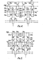
reference numerals PNP transistors 81a through 82b respectively, 83a, 83b, 84a and 84b designate switching NPN transistors for controlling charging currents tophototransistors load resistance load resistances - Next, explanation will be given on a third embodiment of the invention in accordance with Fig. 5, in which a decoder output unit, switching transistors and phototransistors, are connected with each other. In the same drawing,
reference numerals phototransistors load resistances 92a through 93b. In this case, the collectors of switching NPN transistors are connected to the emitters of phototransistors respectively, the collectors thereof being con-. nected in common to form avideo output terminal 98. Hence, for the bipolar integrated circuit technique, separate regions need not be interposed between the respective phototransistors, thereby enabling the space density of phototransistor to be raised. - Next, explanation will be given on a fourth embodiment of the invention in accordance with Fig. 6, in which
reference numeral 99 designates a decoder unit the same as the first embodiment, 100a, 100b, 101a and 101b designate load resistances connected to the outputs of decoders respectively, 102a, 102b, 103a and 103b designate switching PNP transistors, 104a, 104b, 105a and 105b designate load resistances for the switchingPNP transistors 102a through 103a, and 106a, 106b, 107a and 107b designate switching NPN transistors for controlling on or off charging currents tophototransistors load resistance phototransistors NPN transistors 106a through 107b respectively and at the collectors in common. Thephototransistors NPN transistors 106a through 107b, and at the collectors in common, thereby forming a secondvideo output terminal 113. Incidentally, the separate regions between the respective phototransistors, similarly to the former embodiment, need not be interposed between the phototransistors connected at the collectors in common. One phototransistor array is provided with a light-receiving window and the other phototransistor array is light-shielded so that the video output signal is obtained from the common collector terminal at the phototransistors at the light receiving side and noise and dark signal output are obtained from the common collector terminal of phototransistors at the light shielding side, whereby a signal difference is picked up from both the terminals to enable cancellation of noise and dark signal caused by the noise current and the leakage current. The differential signal can be obtained by adifferential amplifier 201. - Referring to Fig. 7, a driving circuit for the image sensor of the invention is shown, which comprises a
timing controller 114, binary counters 115, acode converter 116, ashift register 117, and animage sensor 118. The driving circuit is given the start signal and clock signal from the system side, thetiming controller 114 synchronizing start pulse (ST) with clock pulse, the counter 115 counting up the pulses up to the dot number of image sensor, and thecode converter 116 converting a desired bit output (input bit of decoder) at the LSB side into the code in which the changed bit number of input signal is 1 during the scanning on the adjacent sensor, and thereafter applying the converted code into thedecoder input terminals 119 within the image sensor. Block selecting input signals 120 are given from the output ofshift register 117 shifting at the timing of carry of decoder input signal. Alternatively, in the driving circuit, the scanning in the reverse direction may be applicable in such a manner that the counters may be put in a down count mode and the shift register may shift at the timing of borrow of decoder input signal, thus making it possible to read the original in the reverse direction. - The above embodiments can be made using bipolar techniques.
Claims (20)
Applications Claiming Priority (4)
| Application Number | Priority Date | Filing Date | Title |
|---|---|---|---|
| JP200294/83 | 1983-10-26 | ||
| JP58200294A JPS6091758A (en) | 1983-10-26 | 1983-10-26 | Image sensor |
| JP976/84 | 1984-01-06 | ||
| JP59000976A JPS60144070A (en) | 1984-01-06 | 1984-01-06 | Color image sensor |
Publications (3)
| Publication Number | Publication Date |
|---|---|
| EP0141486A2 true EP0141486A2 (en) | 1985-05-15 |
| EP0141486A3 EP0141486A3 (en) | 1988-07-20 |
| EP0141486B1 EP0141486B1 (en) | 1991-09-11 |
Family
ID=26334101
Family Applications (1)
| Application Number | Title | Priority Date | Filing Date |
|---|---|---|---|
| EP84303897A Expired - Lifetime EP0141486B1 (en) | 1983-10-26 | 1984-06-08 | Image sensor |
Country Status (3)
| Country | Link |
|---|---|
| US (1) | US4567529A (en) |
| EP (1) | EP0141486B1 (en) |
| DE (1) | DE3485050D1 (en) |
Cited By (4)
| Publication number | Priority date | Publication date | Assignee | Title |
|---|---|---|---|---|
| FR2594544A1 (en) * | 1986-02-17 | 1987-08-21 | Messerschmitt Boelkow Blohm | Device with photoelectric sensors with compensation for the dark current |
| EP0234909A2 (en) * | 1986-02-26 | 1987-09-02 | Matsushita Electric Industrial Co., Ltd. | Image sensor |
| EP0437340A2 (en) * | 1990-01-10 | 1991-07-17 | Seiko Instruments Inc. | Image sensor |
| EP0456193A2 (en) * | 1990-05-09 | 1991-11-13 | Matsushita Electric Industrial Co., Ltd. | Image pickup apparatus and counter circuit used therein |
Families Citing this family (18)
| Publication number | Priority date | Publication date | Assignee | Title |
|---|---|---|---|---|
| CA1263175A (en) * | 1984-05-28 | 1989-11-21 | Hideyuki Miyazawa | Image reader for image processing apparatus |
| JPS6154756A (en) * | 1984-08-25 | 1986-03-19 | Fuji Electric Corp Res & Dev Ltd | Contact type image sensor |
| US4763189A (en) * | 1984-08-31 | 1988-08-09 | Canon Kabushiki Kaisha | Color image sensor with three line sensors on different layers separated by electrically-insulating layers |
| JPS62293384A (en) * | 1986-06-11 | 1987-12-19 | Toshiba Corp | Picture input device |
| DE3804200A1 (en) * | 1988-02-11 | 1989-08-24 | Messerschmitt Boelkow Blohm | Photoelectric line sensor |
| US5128778A (en) * | 1990-09-28 | 1992-07-07 | Xerox Corporation | Fast scan imaging area optimization system |
| US6786420B1 (en) | 1997-07-15 | 2004-09-07 | Silverbrook Research Pty. Ltd. | Data distribution mechanism in the form of ink dots on cards |
| US6618117B2 (en) * | 1997-07-12 | 2003-09-09 | Silverbrook Research Pty Ltd | Image sensing apparatus including a microcontroller |
| US6879341B1 (en) | 1997-07-15 | 2005-04-12 | Silverbrook Research Pty Ltd | Digital camera system containing a VLIW vector processor |
| US7551201B2 (en) | 1997-07-15 | 2009-06-23 | Silverbrook Research Pty Ltd | Image capture and processing device for a print on demand digital camera system |
| US7110024B1 (en) | 1997-07-15 | 2006-09-19 | Silverbrook Research Pty Ltd | Digital camera system having motion deblurring means |
| US6690419B1 (en) * | 1997-07-15 | 2004-02-10 | Silverbrook Research Pty Ltd | Utilising eye detection methods for image processing in a digital image camera |
| US6624848B1 (en) * | 1997-07-15 | 2003-09-23 | Silverbrook Research Pty Ltd | Cascading image modification using multiple digital cameras incorporating image processing |
| US6014160A (en) * | 1998-03-30 | 2000-01-11 | Xerox Corporation | Image scanning array having independently addressable photosensor chips |
| AUPP702098A0 (en) | 1998-11-09 | 1998-12-03 | Silverbrook Research Pty Ltd | Image creation method and apparatus (ART73) |
| AUPQ056099A0 (en) * | 1999-05-25 | 1999-06-17 | Silverbrook Research Pty Ltd | A method and apparatus (pprint01) |
| US6796955B2 (en) * | 2002-02-14 | 2004-09-28 | Chf Solutions, Inc. | Method to control blood and filtrate flowing through an extracorporeal device |
| US7164506B2 (en) * | 2002-06-07 | 2007-01-16 | Xerox Corporation | Multi-chip image sensor, on chip apparatus for causing each chip to selectably function in a parallel or serial readout |
Citations (3)
| Publication number | Priority date | Publication date | Assignee | Title |
|---|---|---|---|---|
| US4141018A (en) * | 1976-11-08 | 1979-02-20 | Tokyo Shibaura Electric Co., Ltd. | Thermal recording head and drive circuit |
| US4352128A (en) * | 1977-07-14 | 1982-09-28 | Ricoh Company, Ltd. | Combination electrostatic copying machine and facsimile transceiver |
| FR2508746A1 (en) * | 1981-06-25 | 1982-12-31 | Nippon Telegraph & Telephone | IMAGE SENSOR |
Family Cites Families (5)
| Publication number | Priority date | Publication date | Assignee | Title |
|---|---|---|---|---|
| FR2356328A1 (en) * | 1976-06-24 | 1978-01-20 | Ibm France | NOISE ELIMINATION DEVICE IN SELF-SCANNING PHOTOSENSITIVE NETWORKS |
| JPS5518151A (en) * | 1978-07-26 | 1980-02-08 | Canon Inc | Input device of photo electric conversion information |
| US4237383A (en) * | 1978-09-20 | 1980-12-02 | Rca Corporation | High speed loading of output register of CCD array system |
| US4405857A (en) * | 1980-03-31 | 1983-09-20 | Canon Kabushiki Kaisha | Solid-state photoelectric converter |
| US4495409A (en) * | 1982-02-16 | 1985-01-22 | Hitachi, Ltd. | Photosensor with diode array |
-
1984
- 1984-06-05 US US06/617,566 patent/US4567529A/en not_active Expired - Fee Related
- 1984-06-08 EP EP84303897A patent/EP0141486B1/en not_active Expired - Lifetime
- 1984-06-08 DE DE8484303897T patent/DE3485050D1/en not_active Expired - Lifetime
Patent Citations (3)
| Publication number | Priority date | Publication date | Assignee | Title |
|---|---|---|---|---|
| US4141018A (en) * | 1976-11-08 | 1979-02-20 | Tokyo Shibaura Electric Co., Ltd. | Thermal recording head and drive circuit |
| US4352128A (en) * | 1977-07-14 | 1982-09-28 | Ricoh Company, Ltd. | Combination electrostatic copying machine and facsimile transceiver |
| FR2508746A1 (en) * | 1981-06-25 | 1982-12-31 | Nippon Telegraph & Telephone | IMAGE SENSOR |
Non-Patent Citations (1)
| Title |
|---|
| 1975 IEEE INTERNATIONAL SOLID-STATE CIRCUITS CONFERENCE, DIGEST OF TECHNICAL PAPERS, February 1975, pages 26,27, New York, US; N. KOIKE et al.: "An ultra high-speed clock-pulseless scanner for MOS image sensors" * |
Cited By (9)
| Publication number | Priority date | Publication date | Assignee | Title |
|---|---|---|---|---|
| FR2594544A1 (en) * | 1986-02-17 | 1987-08-21 | Messerschmitt Boelkow Blohm | Device with photoelectric sensors with compensation for the dark current |
| EP0234909A2 (en) * | 1986-02-26 | 1987-09-02 | Matsushita Electric Industrial Co., Ltd. | Image sensor |
| EP0234909A3 (en) * | 1986-02-26 | 1990-01-24 | Matsushita Electric Industrial Co., Ltd. | Image sensor |
| EP0437340A2 (en) * | 1990-01-10 | 1991-07-17 | Seiko Instruments Inc. | Image sensor |
| EP0437340A3 (en) * | 1990-01-10 | 1992-01-02 | Seiko Instruments Inc. | Image sensor |
| US5151587A (en) * | 1990-01-10 | 1992-09-29 | Seiko Instruments Inc. | Image sensor having an array of operative and dummy bipolar transistors and pairs of pixel selecting switches connected thereto |
| EP0456193A2 (en) * | 1990-05-09 | 1991-11-13 | Matsushita Electric Industrial Co., Ltd. | Image pickup apparatus and counter circuit used therein |
| EP0456193A3 (en) * | 1990-05-09 | 1992-11-25 | Matsushita Electric Industrial Co., Ltd. | Image pickup apparatus and counter circuit used therein |
| US5191425A (en) * | 1990-05-09 | 1993-03-02 | Matsushita Electric Industrial Co., Ltd. | Image pickup apparatus having a gray counter |
Also Published As
| Publication number | Publication date |
|---|---|
| EP0141486B1 (en) | 1991-09-11 |
| US4567529A (en) | 1986-01-28 |
| DE3485050D1 (en) | 1991-10-17 |
| EP0141486A3 (en) | 1988-07-20 |
Similar Documents
| Publication | Publication Date | Title |
|---|---|---|
| EP0141486B1 (en) | Image sensor | |
| US6271785B1 (en) | CMOS imager with an A/D per pixel convertor | |
| US5650864A (en) | Full color single-sensor-array contact image sensor (CIS) using advanced signal processing techniques | |
| EP0493455B1 (en) | I.c. sensor | |
| EP0272152B1 (en) | Signal reading out circuit | |
| US7408683B2 (en) | Image sensor for reading image and image reading apparatus including the image sensor | |
| KR100616074B1 (en) | Autocalibration of an a/d converter within an cmos type image sensor | |
| US4413283A (en) | Solid-state imaging device | |
| US5027226A (en) | Contact type image sensor | |
| US4634886A (en) | Photoelectric imager with a high S/N ratio | |
| US6657664B2 (en) | Solid-state image pickup device | |
| US7262801B2 (en) | Image processing apparatus having multiple resolutions | |
| US4704632A (en) | Electronic camera for digital processing of CCD data | |
| JPH09205518A (en) | Image sensor and image sensor chip | |
| US20050094222A1 (en) | High resolution, high sensitivity image scanner having noise cancellation improvements | |
| JPH0215147B2 (en) | ||
| US5109155A (en) | Semiconductor image sensor with an integrated voltage regulator | |
| US7218350B2 (en) | Image sensor with digital output and inherent pixel non-uniformity suppression | |
| JPH063960B2 (en) | Bipolar IC image sensor | |
| US4845567A (en) | Image sensor | |
| JPS61214657A (en) | Image sensor | |
| JPS6126361A (en) | Image sensor | |
| JP2000299762A (en) | Image sensor unit and image reader using the sensor unit | |
| EP0624973A2 (en) | Image sensor | |
| JPS6091758A (en) | Image sensor |
Legal Events
| Date | Code | Title | Description |
|---|---|---|---|
| PUAI | Public reference made under article 153(3) epc to a published international application that has entered the european phase |
Free format text: ORIGINAL CODE: 0009012 |
|
| AK | Designated contracting states |
Designated state(s): DE FR GB NL |
|
| PUAL | Search report despatched |
Free format text: ORIGINAL CODE: 0009013 |
|
| AK | Designated contracting states |
Kind code of ref document: A3 Designated state(s): DE FR GB NL |
|
| 17P | Request for examination filed |
Effective date: 19890113 |
|
| 17Q | First examination report despatched |
Effective date: 19900510 |
|
| GRAA | (expected) grant |
Free format text: ORIGINAL CODE: 0009210 |
|
| AK | Designated contracting states |
Kind code of ref document: B1 Designated state(s): DE FR GB NL |
|
| PG25 | Lapsed in a contracting state [announced via postgrant information from national office to epo] |
Ref country code: NL Effective date: 19910911 |
|
| REF | Corresponds to: |
Ref document number: 3485050 Country of ref document: DE Date of ref document: 19911017 |
|
| ET | Fr: translation filed | ||
| NLV1 | Nl: lapsed or annulled due to failure to fulfill the requirements of art. 29p and 29m of the patents act | ||
| PLBE | No opposition filed within time limit |
Free format text: ORIGINAL CODE: 0009261 |
|
| STAA | Information on the status of an ep patent application or granted ep patent |
Free format text: STATUS: NO OPPOSITION FILED WITHIN TIME LIMIT |
|
| 26N | No opposition filed | ||
| PGFP | Annual fee paid to national office [announced via postgrant information from national office to epo] |
Ref country code: GB Payment date: 19940601 Year of fee payment: 11 |
|
| PGFP | Annual fee paid to national office [announced via postgrant information from national office to epo] |
Ref country code: DE Payment date: 19940608 Year of fee payment: 11 |
|
| PGFP | Annual fee paid to national office [announced via postgrant information from national office to epo] |
Ref country code: FR Payment date: 19940609 Year of fee payment: 11 |
|
| PG25 | Lapsed in a contracting state [announced via postgrant information from national office to epo] |
Ref country code: GB Effective date: 19950608 |
|
| GBPC | Gb: european patent ceased through non-payment of renewal fee |
Effective date: 19950608 |
|
| PG25 | Lapsed in a contracting state [announced via postgrant information from national office to epo] |
Ref country code: FR Effective date: 19960229 |
|
| PG25 | Lapsed in a contracting state [announced via postgrant information from national office to epo] |
Ref country code: DE Effective date: 19960301 |
|
| REG | Reference to a national code |
Ref country code: FR Ref legal event code: ST |