EP0125002A2 - Programmable longitudinal time code generator utilizing a synchronous programmable parallel-to-serial data converter. - Google Patents
Programmable longitudinal time code generator utilizing a synchronous programmable parallel-to-serial data converter. Download PDFInfo
- Publication number
- EP0125002A2 EP0125002A2 EP84302202A EP84302202A EP0125002A2 EP 0125002 A2 EP0125002 A2 EP 0125002A2 EP 84302202 A EP84302202 A EP 84302202A EP 84302202 A EP84302202 A EP 84302202A EP 0125002 A2 EP0125002 A2 EP 0125002A2
- Authority
- EP
- European Patent Office
- Prior art keywords
- programmable
- signal
- time code
- count
- coupled
- Prior art date
- Legal status (The legal status is an assumption and is not a legal conclusion. Google has not performed a legal analysis and makes no representation as to the accuracy of the status listed.)
- Granted
Links
Images


Classifications
-
- G—PHYSICS
- G06—COMPUTING; CALCULATING OR COUNTING
- G06F—ELECTRIC DIGITAL DATA PROCESSING
- G06F13/00—Interconnection of, or transfer of information or other signals between, memories, input/output devices or central processing units
- G06F13/38—Information transfer, e.g. on bus
-
- G—PHYSICS
- G11—INFORMATION STORAGE
- G11B—INFORMATION STORAGE BASED ON RELATIVE MOVEMENT BETWEEN RECORD CARRIER AND TRANSDUCER
- G11B27/00—Editing; Indexing; Addressing; Timing or synchronising; Monitoring; Measuring tape travel
- G11B27/10—Indexing; Addressing; Timing or synchronising; Measuring tape travel
- G11B27/19—Indexing; Addressing; Timing or synchronising; Measuring tape travel by using information detectable on the record carrier
- G11B27/28—Indexing; Addressing; Timing or synchronising; Measuring tape travel by using information detectable on the record carrier by using information signals recorded by the same method as the main recording
- G11B27/32—Indexing; Addressing; Timing or synchronising; Measuring tape travel by using information detectable on the record carrier by using information signals recorded by the same method as the main recording on separate auxiliary tracks of the same or an auxiliary record carrier
- G11B27/322—Indexing; Addressing; Timing or synchronising; Measuring tape travel by using information detectable on the record carrier by using information signals recorded by the same method as the main recording on separate auxiliary tracks of the same or an auxiliary record carrier used signal is digitally coded
- G11B27/323—Time code signal, e.g. on a cue track as SMPTE- or EBU-time code
-
- H—ELECTRICITY
- H03—ELECTRONIC CIRCUITRY
- H03M—CODING; DECODING; CODE CONVERSION IN GENERAL
- H03M9/00—Parallel/series conversion or vice versa
-
- G—PHYSICS
- G11—INFORMATION STORAGE
- G11B—INFORMATION STORAGE BASED ON RELATIVE MOVEMENT BETWEEN RECORD CARRIER AND TRANSDUCER
- G11B2220/00—Record carriers by type
- G11B2220/90—Tape-like record carriers
Landscapes
- Engineering & Computer Science (AREA)
- Theoretical Computer Science (AREA)
- Physics & Mathematics (AREA)
- General Engineering & Computer Science (AREA)
- General Physics & Mathematics (AREA)
- Television Signal Processing For Recording (AREA)
- Signal Processing For Digital Recording And Reproducing (AREA)
- Synchronizing For Television (AREA)
Abstract
Description
- The invention relates to a synchronous programmable parallel-to-serial data converter having a programmable frequency ratio between a parallel input data and serial output data and to a programmable longitudinal time code generator utilizing the converter and which can be programmed for use in various magnetic recording systems and at selected tape speeds.
- As well known in the art of magnetic recording and reproduction, a time code is generally recorded on the magnetic medium, for example tape, along with the information signal. The recorded time code is utilized to locate a portion of the recorded information if necessary for example for editing, video program production or other purposes. For example when providing broadcast quality video tape recording, generation and recording of a time code must conform to specific well defined standards. As it is well known these standards vary with different recording systems, such as NTSC, PAL, PAL-M, SECAM, etc.
- It is well known to utilize for example a microprocessor to generate a time code in parallel form which then must be converted into serial data for recording on tape as a longitudinal time code. In video tape recording, such as utilizing a longitudinal, transverse or helical recording/reproducing format time code is known to be recorded as a longitudinal signal on an audio track by an audio transducer. As well known and in accordance with the above-indicated standards, the time code is measured as an arbritrary time of the day and it consists for all the above-indicated recording systems of 80 bits of which each group of 8-bits or a byte indicates among other values a particular value as follows: tens of hours; units of hours; tens of minutes; units of minutes; tens of seconds; units of seconds; tens of frames and units of frames, respectively. Consequently, when it is necessary to change the recording format or, alternatively, when it is desired to record the time code at slower or faster tape speed than normal playback speed, the parameters of the time code generation must be changed accordingly, to obtain synchronous recording thereof with the recorded information.
- Prior art time code generators utilize relatively complex timing and pulse generating circuitry which cannot be readily modified to provide respective time codes adapted to the above-indicated changes of the recording parameters.
- One aspect of the present invention is a relatively simple device and method for generating a time code which can be readily modified to conform to changes in the recording parameters.
- A more general aspect of the invention is a synchronous programmable parallel-to-serial data converter which may be utilized for synchronous conversion of parallel data into serial form.
- It is a particular object of the present invention to provide a time code generator which can be readily modified to obtain longitudinal time code for synchronous magnetic recording with an information signal recorded in NTSC, PAL, PAL-M, SECAM or other recording formats and at various speeds of magnetic media with respect to normal playback speed.
- The foregoing and other objects, features and advantages of the present invention will be apparent from the following detailed description and accompanying drawings.
-
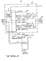
- FIGURE 1 is a simplified block diagram of a preferred embodiment of a synchronous programmable parallel-to-serial data converter circuit in accordance with the present invention.
- FIGURE 2 is a detailed diagram of a preferred embodiment of a programmable longitudinal time code generator in accordance with the present invention utilizing the converter of FIGURE 1.
- FIGURE 3 shows timing diagrams illustrating operation of the circuit of FIGURE l;
- FIGURE 4 shows timing diagrams illustrating operation of the circuit of FIGURE 2; and
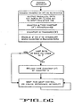
- FIGURES 5A to 5C show simplified flow diagrams depicting the flow of operation of the circuit of FIGURE 2.
- The preferred embodiment of the synchronous programmable parallel-to-serial data converter shown in the block diagram of FIGURE 1 will be now described, followed by a description of the operation thereof with reference to the timing diagrams of FIGURE 3.
- FIGURE 1 shows a first
programmable counter 10 which is connected by aparallel data line 12 to aprogrammable logic circuit 14.Circuit 14 has aninput control line 16 for receiving a synchronization signal A from an outside source (not shown). A secondprogrammable counter 20 is connected tocircuit 14 by aparallel data line 22. Theprogrammable counters control logic circuit 14 by therespective control lines lines 23; 25 represent respective load control signals ofcounters 10; 20, whilelines 26; 26 are respective output control signals from these counters as it will be described in more detail later. - The
control circuit 14 receives a parallel data in the form of parallel data words via adata line 15 from an outside source (not shown). A parallel-to-serial data converter 28, implemented for example by a parallel-to-serial shift register receives that parallel data from thecontrol circuit 14 via aparallel data line 31 and the resulting serial data is obtained therefrom on anoutput data line 32. Theshift register 28 also receives a parallel data input or load control signal E from thelogic circuit 14 via acontrol line 29 and a serial data shift control signal F via acontrol line 30. - Now the operation of the circuit of FIGURE 1 will be described with reference to the timing diagrams of FIGURE 3. The programmable
control logic circuit 14 receives the synchronization pulse A vialine 16 for example from an outside source (not shown), such as a microprocessor as it is well known in the art. Pulse A has a period Tl as depicted in FIGURE 3.Circuit 14 provides in response thereto a load and reset control pulse B vialines programmable counters data line 12 intocounter 10 and a binary number S representing a second integral count is loaded in parallel viadata line 22 intocounter 20 to preset these respective counters. In the preferred embodiment numbers P, S are selected such that P is an integral multiple of S and both counters have the same clock signal frequency which is applied thereto from an lexternalreference clock generator 27 in a well known manner. Counter 10 is preferably implemented as a retriggerable down counter which counts down from number P until it reaches zero and then it provides an output signal C online 24 which re-starts counting bycounter 10 from number P again. Thesecond counter 20 is preferably a free running retriggerable counter which counts continuously at a frequency given by number S and the counter clock rate. The output signal online 26 fromcounter 20 is shown at D in FIGURE 4. - Thus a time interval T2 of output signal C on
line 24 fromcounter 10 is determined by the number P loaded therein and the particular clock frequency utilized. Similarly, a time interval T3 of the output signal D ofcounter 20 is determined by the number S and thecounter 20 clock frequency. - The
programmable control circuit 14 of FIGURE 1 receives a parallel data online 15 from an external source, for example a microprocessor (not shown) as is well known in the art. Each parallel word which in the preferred embodiment is for example 8 bits long, is loaded in theshift register 28 synchronously with the load control signal E, also referred to as parallel clock signal which is derived from signal C by thecontrol logic circuit 14 to obtain correct synchronization. Subsequently,shift register 28 receives the signal F online 30 as a serial data output clock signal which determines the frequency at which the serial output data is shifted out from theshift register 28 online 32. Similarly, the signal F, also referred to as a serial data shift signal is synchronously derived from the above-described output signal D online 26 from the secondprogrammable counter 20 by the programmablecontrol logic circuit 14. It is noted that inherent delays occurring between the various signals due to system operation delays are not shown in the attached timing diagrams to simplify the description. - In addition to
counter 20 being periodically retriggered by signal B, it is also periodically retriggered in response to signal C vialines control logic circuit 14 to obtain additional synchronization. - It is seen from the foregoing description that by selecting the numbers P and S such that at a known clock signal frequency provided by
clock signal generator 27 respective desired time intervals T2, T3 may be obtained which have respective desired integral ratios with reference to the time interval Tl of the synchronization signal. It also follows from the foregoing disclosure that when the frequency of the serial data shift signal F is selected as an integral number multiple of the parallel clock signal E frequency, which number in turn corresponds to the number of bits in a parallel data word online 31, then a synchronous parallel-to-serial data transfer will be obtained. - As it will follow from a more detailed description below, the aforementioned synchronous data conversion in accordance with the present invention is controlled by a programmable control logic circuit which provides accurate synchronization of data transfer throughout the device in a relatively simple manner. It is a particular advantage of the synchronous converter of FIGURE 1 that when it is necessary to change the respective frequency or phase relationship of any of the signals, such change can be easily obtained without modification of the circuit elements.
- As an example, the
programmable counter shift register 28 by an integrated circuit device, type 74LS165, manufactured by Texas Instruments among others. The above-indicated device is indicated in FIGURE 1 by interrupted line and designated byreference numeral 37. - Now the preferred embodiment of a time code generator utilizing a programmable parallel-to-serial converter as previously described with reference to FIGURE 1 will be described in detail with reference to the schematic circuit diagram of FIGURE 2 and the timing diagrams of FIGURE 4.
- In the embodiment of FIGURE 2 a programmable counter/timer input/output device, further referred to as
CTIO device 37 is utilized, preferably implemented by type Z8536 manufactured by Zilog Corporation. The above-indicateddevice 37 has three 16-bit programmable counter/ timer circuits two of which are utilized as a first and asecond counter device 37 also includes a programmable control logic circuit such ascircuit 14 of FIGURE 1, a bidirectional data bus, two sets of 8-bit programmable input/output ports, and one 4-bit port shortly I/O ports, The time code is received ondata bus 15 as a sequence of parallel bytes, for example from a well known time code generator, such as a microprocessor (not shown). Oneset 31 of 8-bit ports is programmed to apply the latter parallel input data to the previously describedshift register 28 of FIGURE 1. - It is noted that to facilitate comparison between the drawing FIGURES like elements are designated by like reference numerals.
- Shift
register 28 is preferably implemented in FIGURE 2 as type 74LS165 manufactured among others by Texas Instruments. - As an example, the operation of the programmable time code generator of the preferred embodiment of FIGURE 2 will be now described where an 80-bit time code is received by
data bus 15 as a sequence of ten parallel bytes and it is applied as an 80-bit longitudinal time code online 32 therefrom for recording on a magnetic tape synchronously with a video information signal, recorded for example by a rotary helical type recording device in a manner well known in the art. As it is well known the video frame rate in the NTSC and PAL-M systems approximately 60 frames/per second, while in PAL and SECAM systems it is 50 frame/per second. Consequently, the frequency at which the longitudinal time code is to be recorded in these various systems must change accordingly to obtain accurate timing and synchronization with the recorded information signal. The programmable time code generator of the invention has the advantage that it can be readily adapted to provide the necessary changes in frequency and in a predetermined delay of the time code without changing any circuit elements as it will follow. - As it is well known, in professional broadcast quality video recording the time code recorded on tape must satisfy well defined standard requirements. One requirement is a given predetermined delay, further referred to as tl, which is a time interval between a specified edge of the vertical sync pulse and the time when actual recording of a video information signal pertaining to the current frame starts. Consequently recording of the time code must be likewise delayed following each vertical sync pulse by a different value of tl as specified for each recording system.
- A further example of a change in recording parameters requiring a corresponding change of the frequency at which the time code is recorded on tape occurs when the recording takes place at a tape speed different from a normal playback speed. For example, when recording at twice the normal tape speed, the time code must be recorded at double frequency. Analogously, when for example the recording takes place at one-half of the normal playback speed, the longitudinal time code frequency must be reduced to one-half to obtain synchronization with the recorded information. It is an important advantage of the time code generator of the present invention that the above indicated changes in the delay and freuency of the longitudinal time code can be readily made without the need of providing relatively complicated timing and logic circuity as it has been the case in prior art time code generators.
- The operation of the programmable time code generator of FIGURE 2 will be described now with reference to flow diagrams of FIGURES 5A to 5C and the timing diagram of FIGURE 4. It is noted that various signals which are comparable to those previously described with reference to FIGURE 3 are indicated in FIGURE 4 by like letter designations with a prime attached thereto while like signals and circuit elements are designated by like characters in all the drawing figures to facilitate comparison.
- First an initialization or power-up of the
programmable CTIO device 37 is provided as depicted in FIGURE 5A. A first counter, selected ascounter 2 of thedevice 37 and which is similar to the previously describedcounter 10 of FIGURE 1 is programmed to be retriggerable. A second counter, selected ascounter 3 of thedevice 37, which is similar to counter 20 of FIGURE 1 is programmed to be continuous, retriggerable and having its output available through port C of thedevice 37, indicated asline 30 in FIGURE 2. Both counters 10, 20 synchronously receive a 2 MHz clock signal obtained from a 4 MHz system clock generator and a frequency divide-by-two (not shown). The system clock generator corresponding toclock signal generator 27 of FIGURE 1. Thereafter a time constant corresponding to a previously described binary number S is programmed for thesecond counter 20 as it will be specified later. Thereafter thecounters CTIO device 37 are enabled. - The following operation will be now described with reference to FIGURE 5B.
- Next, the
CTIO device 37 is programmed to provide a start delay tl every time after a vertical video frame synchronizing pulse A' is received. In the embodiment of FIGURE 2 the signal A' is received as a parallel data byte viadata bus 15 in a time shared manner with the parallel time code data. Signal A' and the start delay tl are shown in the timing diagram of FIGURE 4. Then counter 10 is triggered by a pulse I' and interrupts are enabled to interrupt the operation whencounter 10 reaches zero. It will be understood from the foregoing description that the start delay tl is obtained by loading intocounter 10 for example a number M' whose value is selected to obtain the necessary delay tl at the known clock frequency ofcounter 10. Thus when counter 10 counts down to zero a first interrupt signal B' is provided online 24 by that counter as shown in FIGURE 3. - The following operation is described with reference to FIGURE 5C. In response to signal B' the CTIO device triggers the second
programmable counter 20 and simultaneously the parallel data byte received atinput ports 15 is applied viaoutput ports 31 to a parallel input of the parallel-to-serial converter 28. Simultaneously the previously described binary number P' is programmed by theCTIO device 37 for thefirst counter 10, where P is a 16-th multiple of the number S as previously described, that is P = 16 x S. Thereafter counter 10 is triggered by the previously described pulse B'.Counter 10 interrupt is enabled to allowretriggering counter 20 every time when a zero count is obtained bycounter 10. The latter interrupt or control signal is shown in FIGURE 4 at E'. The CTIO device is programmed to repeat the above-described operations of FIGURES 5A to 5C following the reception of each vertical sync signal A' online 16. - In the preferred embodiment of FIGURE 2 sixteen pulses D' are provided by counter 20 for reach pulse C' for the following reasons. The serial pulses of the longitudinal time code obtained on
line 32 are in the return-to-zero or shortly RZ form. As well known in the art the latter type of signal cannot be easily recovered from tape because of its non-self-clocking format. - Consequently, it is necessary to convert these pulses from RZ to NRZ or non-return-to-zero format by obtaining an additional transition from high to low or low to high value in the middle of each bit cell corresponding to binary one as well known. To obtain the foregoing, the above-described respective signals D' and F' are provided by the circuit of FIGURE 2 at twice the rate at which the serial output signal, that is the longitudinal time code on
line 32 is applied from theshift register 28. The RZ to NRZ conversion is provided by flip-flops NAND gate 42. Flip-flop 40 receives online 30 from theCTIO device 37 signal F' at afrequency 16 times that of signal C'. Flip-flop 40 receives the latter signal and divides its frequency by two. The resulting signal is applied therefrom vialine 30a to the parallel-to-serial shift register 28 as the serial clock signal. The above- mentioned signal F' online 30 is also applied to the second flip-flop 41. Theshift register 28 provides a serial output signal online 32 at its serial clock frequency online 30a which output signal corresponds to the longitudinal time code which however is in the form of an RZ signal. The signal online 32 is then applied through aNAND gate 42 whose other input receives the serial clock signal online 30a to the second flip-flop 41. Flip-flop 41 in turn provides a midcell transition for each serial pulse received on line 32a which has a binary value of one, the timing of that transition being determined by the signal F' online 30. As a result a serial time code signal in the desired NRZ from is obtained onoutput line 32b from flip-flop 41 which output signal is synchronous with signal F' online 30 and has one half of its frequency. - It will be understood from the foreging disclosure that if it is desired to utilize the embodiment of FIGURES 1 or 2 to obtain serial output data at various selected frequency ratios with respect to a synchronizing signal or, alternatively, when it is necessary to change the frequency of the synchronizing signal received by these embodiments, or the delay tl, a plurality of parameters P; S or P'; S' and/or M' may be stored by the programmable control circuit. Selected ones of these parameters are then retrived by the control circuit to obtain the particular selected frequency ratios and/or delay.
- Having described specific preferred embodiments of the invention with reference to the accompanying drawings, it is to be understood that the invention is not limited to those precise embodiments, and that various changes and modifications may be effected therein by one skilled in the art without departing from the scope or spirit of the invention as defined in the appended claims.
Claims (3)
Applications Claiming Priority (2)
| Application Number | Priority Date | Filing Date | Title |
|---|---|---|---|
| US06/483,326 US4532557A (en) | 1983-04-08 | 1983-04-08 | Synchronous programmable parallel-to-serial data converter and a programmable longitudinal time code generator utilizing the converter |
| US483326 | 1983-04-08 |
Publications (3)
| Publication Number | Publication Date |
|---|---|
| EP0125002A2 true EP0125002A2 (en) | 1984-11-14 |
| EP0125002A3 EP0125002A3 (en) | 1987-11-11 |
| EP0125002B1 EP0125002B1 (en) | 1992-10-21 |
Family
ID=23919618
Family Applications (1)
| Application Number | Title | Priority Date | Filing Date |
|---|---|---|---|
| EP84302202A Expired - Lifetime EP0125002B1 (en) | 1983-04-08 | 1984-03-30 | Programmable longitudinal time code generator utilizing a synchronous programmable parallel-to-serial data converter. |
Country Status (4)
| Country | Link |
|---|---|
| US (1) | US4532557A (en) |
| EP (1) | EP0125002B1 (en) |
| JP (1) | JPS59198507A (en) |
| DE (1) | DE3485959T2 (en) |
Cited By (1)
| Publication number | Priority date | Publication date | Assignee | Title |
|---|---|---|---|---|
| EP0245616A2 (en) * | 1986-04-15 | 1987-11-19 | Dr. Johannes Heidenhain GmbH | Apparatus for the serial transfer of digital values from a measurement converter |
Families Citing this family (15)
| Publication number | Priority date | Publication date | Assignee | Title |
|---|---|---|---|---|
| JPS627276A (en) * | 1985-07-04 | 1987-01-14 | Pioneer Video Kk | Video disk and its recorder |
| US4739419A (en) * | 1986-01-06 | 1988-04-19 | Eastman Kodak Company | Apparatus for eliminating midfield skew error by delaying the lower half field of a T M format video signal to be recorded on the second of two tracks |
| JPH01264385A (en) * | 1988-04-15 | 1989-10-20 | Hitachi Ltd | Video signal recording/reproducing device |
| JPH0535442A (en) * | 1991-07-31 | 1993-02-12 | Toshiba Corp | Image data converting circuit |
| JPH0573697A (en) * | 1991-08-30 | 1993-03-26 | Nec Corp | Microcomputer |
| JP3104085B2 (en) * | 1991-10-18 | 2000-10-30 | ソニー株式会社 | Transmission system for recording / reproducing device |
| US5276559A (en) * | 1992-03-27 | 1994-01-04 | Datatape Incorporated | Technique for recording and reproducing low rate data in a helical vehicle scan recorder having a stationary time code signal reproduce magnetic head |
| US5255096B1 (en) * | 1992-04-10 | 1997-12-23 | William M Boyle | Video time code synchronized robot control apparatus |
| JPH06265999A (en) * | 1993-03-12 | 1994-09-22 | Nikon Corp | Camera capable of recording photographing information |
| DE4315301A1 (en) * | 1993-05-07 | 1994-11-10 | Becker Gmbh | Method of operating a player for optical sound carriers |
| KR0161807B1 (en) * | 1995-12-30 | 1998-12-15 | 김광호 | Time code generator circuit |
| JP3189754B2 (en) | 1997-09-16 | 2001-07-16 | 松下電器産業株式会社 | Time code recording device for magnetic recording / reproducing device |
| DE10105857A1 (en) * | 2001-02-08 | 2002-08-14 | Marten Saal | Cascadeable input output decoder for connection to a PC, etc. via serial, parallel or USB interface, has a modular design and onboard processor on first module to greatly speed input and output |
| DE10228905A1 (en) | 2002-06-27 | 2004-01-15 | Robert Bosch Gmbh | Method and device for data transmission |
| US7197053B1 (en) * | 2003-03-05 | 2007-03-27 | Applied Micro Circuits Corporation | Serializer with programmable delay elements |
Citations (3)
| Publication number | Priority date | Publication date | Assignee | Title |
|---|---|---|---|---|
| US3681524A (en) * | 1970-06-16 | 1972-08-01 | Columbia Broadcasting Syst Inc | Multiple frequency time code generator and reader |
| US4159480A (en) * | 1976-10-27 | 1979-06-26 | Sony Corporation | Method of inserting an address signal in a video signal |
| US4175267A (en) * | 1976-07-30 | 1979-11-20 | Sony Corporation | Method and apparatus of inserting an address signal in a video signal |
Family Cites Families (1)
| Publication number | Priority date | Publication date | Assignee | Title |
|---|---|---|---|---|
| US4134130A (en) * | 1976-07-30 | 1979-01-09 | Sony Corporation | Method and apparatus of inserting an address signal in a video signal |
-
1983
- 1983-04-08 US US06/483,326 patent/US4532557A/en not_active Expired - Lifetime
-
1984
- 1984-03-30 EP EP84302202A patent/EP0125002B1/en not_active Expired - Lifetime
- 1984-03-30 DE DE8484302202T patent/DE3485959T2/en not_active Expired - Fee Related
- 1984-04-06 JP JP59068967A patent/JPS59198507A/en active Pending
Patent Citations (3)
| Publication number | Priority date | Publication date | Assignee | Title |
|---|---|---|---|---|
| US3681524A (en) * | 1970-06-16 | 1972-08-01 | Columbia Broadcasting Syst Inc | Multiple frequency time code generator and reader |
| US4175267A (en) * | 1976-07-30 | 1979-11-20 | Sony Corporation | Method and apparatus of inserting an address signal in a video signal |
| US4159480A (en) * | 1976-10-27 | 1979-06-26 | Sony Corporation | Method of inserting an address signal in a video signal |
Non-Patent Citations (3)
| Title |
|---|
| PHILIPS DATA HANDBOOK, Signetics Integrated Circuits, 1978, page 275, 54/74 Series "165". * |
| SMPTE JOURNAL, vol. 88, no. 12, December 1979, pages 831-834, Scarsdale, US; H.D. GEISE: "The use of microcomputers and microprocessors in modern VTR control" * |
| WIRELESS WORLD, vol. 87, no. 1550, November 1981, pages 59-62, Haywards Heath, GB; J.D. FERGUSON et al.: "Interfacing microprocessors" * |
Cited By (2)
| Publication number | Priority date | Publication date | Assignee | Title |
|---|---|---|---|---|
| EP0245616A2 (en) * | 1986-04-15 | 1987-11-19 | Dr. Johannes Heidenhain GmbH | Apparatus for the serial transfer of digital values from a measurement converter |
| EP0245616A3 (en) * | 1986-04-15 | 1989-07-12 | Dr. Johannes Heidenhain Gmbh | Apparatus for the serial transfer of digital values from a measurement converter |
Also Published As
| Publication number | Publication date |
|---|---|
| DE3485959D1 (en) | 1992-11-26 |
| DE3485959T2 (en) | 1993-03-04 |
| JPS59198507A (en) | 1984-11-10 |
| US4532557A (en) | 1985-07-30 |
| EP0125002A3 (en) | 1987-11-11 |
| EP0125002B1 (en) | 1992-10-21 |
Similar Documents
| Publication | Publication Date | Title |
|---|---|---|
| US4532557A (en) | Synchronous programmable parallel-to-serial data converter and a programmable longitudinal time code generator utilizing the converter | |
| US4387364A (en) | Method and apparatus for reducing DC components in a digital information signal | |
| US4353130A (en) | Device for processing serial information which includes synchronization words | |
| US4750173A (en) | Method of transmitting audio information and additional information in digital form | |
| US5757871A (en) | Jitter suppression circuit for clock signals used for sending data from a synchronous transmission network to an asynchronous transmission network | |
| GB2181325A (en) | Synchronising audio and video signals of a television transmission | |
| CA2031055A1 (en) | Programmable multiplexing techniques for mapping a capacity domain into a time domain within a frame | |
| US4423440A (en) | Code signal reading apparatus | |
| JPH0118615B2 (en) | ||
| US4500871A (en) | Method for coding binary data and a device decoding coded data | |
| EP0290851A2 (en) | Synchronizing clock signal generator | |
| US4573172A (en) | Programmable circuit for series-parallel transformation of a digital signal | |
| KR0161807B1 (en) | Time code generator circuit | |
| KR940001272B1 (en) | System transmitting and checking data | |
| US4636877A (en) | Apparatus for reproducing multiple track digital signals and including timing control of read/write operations | |
| US4825303A (en) | Compressed audio silencing | |
| US4887261A (en) | Method and arrangement for transmitting a digital signal with a low bit rate in a time section, provided for higher bit rates, of a time division multiplexed signal | |
| US4063291A (en) | Apparatus and method for encoding and decoding digital information | |
| US4300173A (en) | Data recording and reading circuitry | |
| JPS6316471A (en) | Reproducing device for digital data | |
| JP2697629B2 (en) | Speed converter | |
| JP2535393B2 (en) | Sync signal detection circuit | |
| SU1474660A1 (en) | Tape unit/computer interface | |
| JP2594765B2 (en) | Time division multiplex circuit | |
| JPS5894254A (en) | Digital signal transmitter |
Legal Events
| Date | Code | Title | Description |
|---|---|---|---|
| PUAI | Public reference made under article 153(3) epc to a published international application that has entered the european phase |
Free format text: ORIGINAL CODE: 0009012 |
|
| AK | Designated contracting states |
Kind code of ref document: A2 Designated state(s): CH DE FR GB LI NL Designated state(s): CH DE FR GB LI NL |
|
| PUAL | Search report despatched |
Free format text: ORIGINAL CODE: 0009013 |
|
| AK | Designated contracting states |
Kind code of ref document: A3 Designated state(s): CH DE FR GB LI NL |
|
| 17P | Request for examination filed |
Effective date: 19880516 |
|
| 17Q | First examination report despatched |
Effective date: 19890811 |
|
| RTI1 | Title (correction) | ||
| GRAA | (expected) grant |
Free format text: ORIGINAL CODE: 0009210 |
|
| RBV | Designated contracting states (corrected) |
Designated state(s): DE FR GB NL |
|
| AK | Designated contracting states |
Kind code of ref document: B1 Designated state(s): DE FR GB NL |
|
| REF | Corresponds to: |
Ref document number: 3485959 Country of ref document: DE Date of ref document: 19921126 |
|
| ET | Fr: translation filed | ||
| PLBE | No opposition filed within time limit |
Free format text: ORIGINAL CODE: 0009261 |
|
| STAA | Information on the status of an ep patent application or granted ep patent |
Free format text: STATUS: NO OPPOSITION FILED WITHIN TIME LIMIT |
|
| 26N | No opposition filed | ||
| REG | Reference to a national code |
Ref country code: GB Ref legal event code: 732E |
|
| PG25 | Lapsed in a contracting state [announced via postgrant information from national office to epo] |
Ref country code: FR Effective date: 19931130 |
|
| REG | Reference to a national code |
Ref country code: FR Ref legal event code: ST |
|
| PGFP | Annual fee paid to national office [announced via postgrant information from national office to epo] |
Ref country code: GB Payment date: 19940321 Year of fee payment: 11 |
|
| PGFP | Annual fee paid to national office [announced via postgrant information from national office to epo] |
Ref country code: DE Payment date: 19940323 Year of fee payment: 11 |
|
| PGFP | Annual fee paid to national office [announced via postgrant information from national office to epo] |
Ref country code: NL Payment date: 19940331 Year of fee payment: 11 |
|
| NLS | Nl: assignments of ep-patents |
Owner name: AMPEX SYSTEMS CORPORATION TE REDWOOD CITY, CALIFOR |
|
| PG25 | Lapsed in a contracting state [announced via postgrant information from national office to epo] |
Ref country code: GB Effective date: 19950330 |
|
| PG25 | Lapsed in a contracting state [announced via postgrant information from national office to epo] |
Ref country code: NL Effective date: 19951001 |
|
| GBPC | Gb: european patent ceased through non-payment of renewal fee |
Effective date: 19950330 |
|
| NLV4 | Nl: lapsed or anulled due to non-payment of the annual fee |
Effective date: 19951001 |
|
| PG25 | Lapsed in a contracting state [announced via postgrant information from national office to epo] |
Ref country code: DE Effective date: 19951201 |