EP0123922A2 - Instruction buffer bypass apparatus - Google Patents
Instruction buffer bypass apparatus Download PDFInfo
- Publication number
- EP0123922A2 EP0123922A2 EP84103512A EP84103512A EP0123922A2 EP 0123922 A2 EP0123922 A2 EP 0123922A2 EP 84103512 A EP84103512 A EP 84103512A EP 84103512 A EP84103512 A EP 84103512A EP 0123922 A2 EP0123922 A2 EP 0123922A2
- Authority
- EP
- European Patent Office
- Prior art keywords
- instruction
- register
- buffer
- storage facility
- byte
- Prior art date
- Legal status (The legal status is an assumption and is not a legal conclusion. Google has not performed a legal analysis and makes no representation as to the accuracy of the status listed.)
- Granted
Links
Images

Classifications
-
- G—PHYSICS
- G06—COMPUTING; CALCULATING OR COUNTING
- G06F—ELECTRIC DIGITAL DATA PROCESSING
- G06F9/00—Arrangements for program control, e.g. control units
- G06F9/06—Arrangements for program control, e.g. control units using stored programs, i.e. using an internal store of processing equipment to receive or retain programs
- G06F9/30—Arrangements for executing machine instructions, e.g. instruction decode
- G06F9/30181—Instruction operation extension or modification
-
- G—PHYSICS
- G06—COMPUTING; CALCULATING OR COUNTING
- G06F—ELECTRIC DIGITAL DATA PROCESSING
- G06F9/00—Arrangements for program control, e.g. control units
- G06F9/06—Arrangements for program control, e.g. control units using stored programs, i.e. using an internal store of processing equipment to receive or retain programs
- G06F9/30—Arrangements for executing machine instructions, e.g. instruction decode
- G06F9/30003—Arrangements for executing specific machine instructions
- G06F9/3005—Arrangements for executing specific machine instructions to perform operations for flow control
- G06F9/30054—Unconditional branch instructions
-
- G—PHYSICS
- G06—COMPUTING; CALCULATING OR COUNTING
- G06F—ELECTRIC DIGITAL DATA PROCESSING
- G06F9/00—Arrangements for program control, e.g. control units
- G06F9/06—Arrangements for program control, e.g. control units using stored programs, i.e. using an internal store of processing equipment to receive or retain programs
- G06F9/30—Arrangements for executing machine instructions, e.g. instruction decode
- G06F9/30145—Instruction analysis, e.g. decoding, instruction word fields
- G06F9/30149—Instruction analysis, e.g. decoding, instruction word fields of variable length instructions
-
- G—PHYSICS
- G06—COMPUTING; CALCULATING OR COUNTING
- G06F—ELECTRIC DIGITAL DATA PROCESSING
- G06F9/00—Arrangements for program control, e.g. control units
- G06F9/06—Arrangements for program control, e.g. control units using stored programs, i.e. using an internal store of processing equipment to receive or retain programs
- G06F9/30—Arrangements for executing machine instructions, e.g. instruction decode
- G06F9/30181—Instruction operation extension or modification
- G06F9/30185—Instruction operation extension or modification according to one or more bits in the instruction, e.g. prefix, sub-opcode
-
- G—PHYSICS
- G06—COMPUTING; CALCULATING OR COUNTING
- G06F—ELECTRIC DIGITAL DATA PROCESSING
- G06F9/00—Arrangements for program control, e.g. control units
- G06F9/06—Arrangements for program control, e.g. control units using stored programs, i.e. using an internal store of processing equipment to receive or retain programs
- G06F9/30—Arrangements for executing machine instructions, e.g. instruction decode
- G06F9/38—Concurrent instruction execution, e.g. pipeline, look ahead
- G06F9/3802—Instruction prefetching
- G06F9/3816—Instruction alignment, e.g. cache line crossing
Landscapes
- Engineering & Computer Science (AREA)
- Software Systems (AREA)
- Theoretical Computer Science (AREA)
- Physics & Mathematics (AREA)
- General Engineering & Computer Science (AREA)
- General Physics & Mathematics (AREA)
- Advance Control (AREA)
- Executing Machine-Instructions (AREA)
Abstract
Description
- The subject matter of the present invention pertains to a computer system, and more particularly, to a bypass path in a computer system for bypassing an instruction buffer when certain specific instructions are being executed.
- Prior art computer systems, such as that shown in U.S. Patent No. 3,949,379, execute instructions in a predetermined sequence. In such systems, an instruction to be executed is stored in an instruction register. An instruction buffer is connected to the instruction register for storing a next instruction to be executed in the sequence. When execution of the instruction is complete, the next instruction in the sequence, stored in the instruction buffer, is transferred to the instruction register, whereby execution of the next instruction commences. When execution of the next instruction begins, a further instruction in the sequence is stored in the instruction buffer.
- However, certain special instructions, such as an EXECUTE instruction, may appear in the sequence. When a special instruction in the sequence is transferred to the instruction register for execution, another instruction, herein referred to as a "subject instruction", is taken out-of-sequence from the central storage facility and is transferred to the instruction register via the instruction buffer for execution. Since the "subject instruction" is transferred to the instruction register via the instruction buffer, the previous contents of the instruction buffer are destroyed. The previous contents of the instruction buffer include the next instruction to be executed Ln the sequence following execution of the special Lnstruction.
- 3ince the previous contents of the instruction buffer were destroyed, the predetermined sequence of instructions to be executed by the computer system was disrupted. Therefore, it was necessary to re-initialize the instruction buffer, that is, to fetch the next instruction in the sequence from storage and re-store it in the instruction buffer. This re-initialization consumes time and resources.
- In addition, there are instances in which the byte-length of the instruction register is smaller than the byte-length of the instruction to be stored in the instruction register for execution.
- The prior art, such as U.S. Patents 4,268,907, 4,189,770, and IBM Technical Disclosure Bulletin Vol. 23, No. 12, May 1981, pp. 5329-5331 discloses various types of buffer bypass circuitry. However, this prior art fails to disclose, teach, or suggest the invention disclosed in this application, whereby the contents of the instruction buffer, containing the next instruction to be executed in the sequence, are preserved during execution of certain special instructions, such as the EXECUTE instruction.
- A primary object of the present invention involves the elimination of the disadvantages associated with the computer system of the prior art, especially with regard to elimination of the disadvantage involving re-initialization of the instruction buffer associated with said computer system.
- Another object of the present invention includes the provision of an additional register to store one or more bytes of the instruction to be executed when the byte-length of said instruction is larger than the byte-length of the instruction register.
- These and other objects of the present invention are accomplished by creating a bypass path for bypassing the instruction buffer when certain special instructions are executed, such as the EXECUTE instruction, thereby transferring the "subject instruction" from storage to the instruction register via the bypass path in lieu of the instruction buffer. As a result, the previous contents of the instruction buffer, comprising the next instruction to be executed in the sequence, are preserved for execution following execution of the special instruction. Furthermore, an execute register is provided for storing one or more bytes of the subject instruction to be executed when all of the bytes of said instruction cannot be stored in the instruction register.
- A full understanding of the present invention will be obtained from the detailed description given hereinbelow and the accompanying drawings, which are given by way of illustration only, and thus are not limitative of the present invention, and wherein:
- figure 1 illustrates a basic block diagram of a portion of a computer system including an instruction buffer, an instruction register, an execute register, and a bypass path representing one feature of the present invention;
- figure 2 illustrates a sample special instruction in the sequence as executed by the computer system and a sample "subject instruction" taken out'of the sequence and fetched from storage in response to execution of the special instruction, such as said EXECUTE instruction;
- figures 3a illustrate a portion of a prior art through 3f computer system whereby the execution of the special instruction occurs without the utilization of the bypass path of figure 1;
- figures 4a illustrate a portion of the computer through 4d system of the present invention, whereby the execution of the special instruction occurs while utilizing the bypass path of figure 1;
- figures 5a illustrate the basic block diagram of through 5d figure 1 and emphasize the function performed by the execute register representing another feature of the present invention, whereby the byte-length of the instruction register is greater than or equal to the byte-length of the instruction to be executed;
- figures 6a illustrate the basic block diagram of through 6d figure 1 and emphasize the function performed by the execute register representing another feature of the present invention, whereby the byte-length of the instruction register is less than the byte-length of the instruction to be executed; and
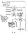
- figure 7 illustrates a flow chart depicting the operation of the block diagram shown in figure 1 of the drawings and further shown in figures 4 through 6 of the drawings.
- Referring to figure 1, a basic block diagram of a portion of a computer system is illustrated. In fig. 1, a
byte shifter 3 receives instructions from a central storage facility within the computer system and aligns the instructions during their transfer through the byte shifter. Aninstruction buffer 9 is connected to thebyte shifter 3 for receiving and temporarily storing instructions from thebyte shifter 3. Aninstruction register 11 is connected to theinstruction buffer 9 and to thebyte shifter 3 viabusses instruction buffer 9 including the special instruction, and for receiving the "subject instruction" viabusses byte shifter 3. Anexecute register 13 is interconnected between thebyte shifter 3 and theinstruction register 11 for temporarily storing one or more additional bytes of the instruction to be executed when the byte-length of the instruction is greater than the byte-length of theinstruction register 11. Acomputer system processor 16 is connected to theinstruction register 11 for receiving the instruction stored in theregister 11 and for executing said instruction. - For further information on a system with which the components of figure 1 interface, reference is directed to a manual entitled "IBM System/370 Principles of Operation" (IBM FORM NO. GA22-7000).
- In operation, referring to figure 1, a
computer system processor 16 executes in sequence a plurality of instructions, each of the instructions being sequentially transferred to theinstruction register 11 via theinstruction buffer 9 for execution. Under normal circumstances, during execution of an instruction stored in the instruction register, the next instruction to be executed in the sequence is stored in theinstruction buffer 9. When execution of the instruction is complete, the next instruction in sequence is retrieved from theinstruction buffer 9, and is stored in theinstruction register 11 for execution. If the next instruction in the sequence is a special instruction, such as an EXECUTE instruction, when the special instruction is executed, another instruction, referred to herein as a "subject instruction", is retrieved from the processor's central storage facility. The subject instruction is not a member of the plurality of instructions sequentially executed by thecomputer system processor 16. Therefore, during the sequential execution of the plurality-of instructions by theprocessor 16, when the special instruction is transferred from theinstruction buffer 9 to theinstruction register 11 for execution, the "subject instruction" is retrieved from the central storage facility, out-of-sequence, is transferred to theinstruction register 11, and is executed by theprocessor 16. When execution of the "subject instruction" is complete, a further instruction in the sequence is transferred to theinstruction register 11 for execution. - In the prior art, the "subject instruction" was taken out of sequence and transferred to the
instruction register 11 via theinstruction buffer 9. As a result of this transfer, the previous contents of theinstruction buffer 9 were destroyed. The previous contents of theinstruction buffer 9 comprises the next instruction in the sequence to be executed following execution of the subject instruction. Since the previous contents were destroyed, re-initialization of theinstruction buffer 9 was necessary - that is, the next instruction in the sequence was again retrieved from the central storage facility and was stored in theinstruction buffer 9. This re-initialization consumed time and resources. - According to the present invention, the "subject instruction" is transferred to the
instruction register 11 viapaths Paths instruction buffer 9 is bypassed during execution of the special instruction. When the "subject instruction" is retrieved from the processor's central storage facility, in response to execution of the special instruction, it is transferred to theinstruction register 11 via the bypass path, that is,paths instruction buffer 9, comprising the next instruction in the sequence to be executed, are not lost or destroyed. Following the execution of the subject instruction, the next instruction in the sequence, stored in theinstruction buffer 9, is transferred from thebuffer 9 to theinstruction register 11 for execution. As a result of utilization of thebypass paths instruction buffer 9 is not necessary. - Referring to figure 2, sample instructions are illustrated. These instructions are intended to be executed in sequence and include
op 0, opl, op3 throughop 7, and the special instruction, namely; the EXECUTE op "Ex op". - In figure 2, a "subject instruction" is also illustrated, retrieved from the processor's central storage facility in response to the execution of the EXECUTE op shown in figure 2.
- The sample instructions of figure 2 will be utilized in a discussion of figures 3 through 6 of the drawings.
- Referring to figure 3a through 3f, a portion of a computer system of the prior art is illustrated representing various steps performed during the execution of the special EXECUTE instruction and the resultant retrieval of the "subject instruction" from the processor's central storage facility. In figure 3a, the EXECUTE op is stored in the
instruction register 11. Theprocessor 16 executes the EXECUTE op instruction. As a result, the address of the "subject instruction" is calculated. In figure 3b, the "subject instruction" is fetched from the central storage facility. In figures 3c and 3d, the "subject instruction" is transferred to theinstruction register 11 via theinstruction buffer 9.Ops instruction buffer 9. As a result, these ops were destroyed during the transfer of the "subject instruction" to theinstruction register 11 viabuffer 9. In figure 3e, these ops are re-fetched from the processor's central storage facility and stored in theinstruction buffer 9, that is, theinstruction buffer 9 is re-initialized. In figure 3f, the next instruction in sequence,op 3, stored in theinstruction register 11, is executed. - Referring to figure 4, a portion of'a computer system of the present invention is illustrated representing various steps performed during the execution of the special EXECUTE instruction and the resultant retrieval of the "subject instruction" from the processor's central storage facility. However, in this figure, the
bypass path buffer 9 to instruction register 11 for storage and execution.Ops buffer 9 and await execution in sequence. In figure 4b, the EXECUTE op is stored in theinstruction register 11 for execution. In response to execution of the EXECUTE op instruction, the "subject instruction" is fetched from the processor central storage facility. In figure 4c, the "subject instruction" is transferred to and loaded into theinstruction register 11 viabyte shifter 3 andbypass paths op 3, is transferred frombuffer 9 to theinstruction register 11 for execution. Therefore, re-initialization of theinstruction buffer 9 is not necessary. - An additional feature of the present invention will be described in the paragraphs to follow.
- As previously mentioned, there are instances in which the byte-length of the instruction to be executed is greater than the byte-length of the
instruction register 11 which stores said instruction. One or more additional bytes of the instruction cannot be loaded into theinstruction register 11 for storage. In order to accommodate the one or more additional bytes of the instruction, the executeregister 13 is connected between thebyte shifter 3 and theinstruction register 11 for receiving and storing the one or more additional bytes of the instruction to be executed. For example, if theinstruction register 11 is four bytes in length, and the instruction to be executed is six bytes in length, the low-order two bytes of the instruction are stored in the executeregister 13, and the high-order four bytes of the instruction are stored in theinstruction register 11. The high-order four bytes are processed by theprocessor 16. When processing of the high-order four bytes is complete, the low-order two bytes are loaded into the instruction register 11 from the executeregister 13 for execution by theprocessor 16. To further illustrate the utilization of the executeregister 13 for receiving and storing the one or more additional bytes of the instruction to be executed, refer to figures 5 and 6 of the drawings. - Figure 5 illustrates a condition whereby the instruction to be executed, passing through the
byte shifter 3 possesses a byte-length which is equal to or less than the byte-length of theinstruction register 11. Consequently, the executeregister 13 is not utilized. Theinstruction buffer 9 is not shown in the figure. Figure 5 also illustrates a concept. That is, thebyte shifter 3 comprises a shifting or alignment apparatus for receiving the instructions from the processor's central storage facility, examining the low order bits of the instruction address representing the amount of shift required, and shifting (ie -aligning) the instruction a specified amount depending on the examined address bits of the instruction. For example, in figure 5a, the instruction address is XX---XX000. The last three low order bits of the instruction address are "000" as indicated by element no. 20. As a result, no shifting or alignment of the instruction occurs. In figure 5b, the last three low order bits of the instruction address are "010" as indicated by element no. 22. As a result, the instruction is shifted from a position corresponding tobyte 2 to a position corresponding tobyte 0 as it passes through thebyte shifter 3. In figure 5c, the last three low order bits of the instruction address are "100" as indicated by element no. 24. As a result, the instruction is shifted from a position corresponding tobyte 4 to a position corresponding tobyte 0 as it passes through the byte shifter 3 (in the figure, the shifting occurs from right to left within the byte shifter). - In figure 5a through 5c,
dark lines 18 are shown. These lines are thebypass paths dark lines 18 indicate that one fetch is required to transfer the instruction from the central storage facility to theinstruction register 11 via thebyte shifter 3. However, in figures 5d1 and 5d2, a dark line is shown in each figure. As a result, in figure 5d1, a first fetch is required to transfer a portion of the instruction to theregister 11 viabyte shifter 3. In figure 5d2, a second fetch is required to transfer another portion of the instruction to theregister 11 viabyte shifter 3. Furthermore, in fig. 5d, the last three low order bits of the instruction address are "110" as indicated by element no. 26. As a result, both portions of the instruction are shifted from a position corresponding tobyte 6 to a position corresponding tobyte 0 as they pass through thebyte shifter 3. - In figure 5, since the byte-length of the instruction to be executed is less than or equal to the byte-length of the
instruction register 11, the executeregister 13 is not utilized. However, in figure'6, the byte-length of the instruction to be executed is greater than the byte-length of theinstruction register 11. Therefore, the one or more additional bytes of the instruction are stored in the executeregister 13, while the high order bytes of the instruction are stored in theinstruction register 11 for execution. When the instruction is being processed, the one or more bytes of the instruction are transferred to the instruction register 11 from the executeregister 13 for execution. - In fig. 6, when the instruction passes through the
byte shifter 3 for shifting and alignment, the low order bits of the instruction address are examined. In response thereto, the instruction is shifted, within thebyte shifter 3, by a specific amount in the same manner as described above with reference to figure 5 of the drawings. For example, in figure 6a, the last three bits of the instruction address are "000" as indicated by element no. 28. Therefore, when the instruction passes through thebyte shifter 3, no shifting occurs. One or more bytes of the instruction pass to the executeregister 13 while the high order bytes pass to theinstruction register 11 for execution. Subsequently, the one or more bytes stored in the executeregister 13 pass to theinstruction register 11 for execution. - In figure 6b, the last three bits of the instruction address are "010" as indicated by element no. 30. As a result, when the instruction passes through the
byte shifter 3, it is shifted from a position corresponding tobyte 2 to a position corresponding tobyte 0. The high order bytes of the instruction are transferred to theinstruction register 11 while the low order bytes are transferred to the executeregister 13 in the same manner as described with reference to fig. 6a. - In figure 6c, the
dark lines 18 indicate the transfer of instruction bytes. Utilizing the dark lines to interpret fig. 6c, since the last three bits of the instruction address are "100" as indicated by element no. 32, during a first fetch of the high order bytes of the instruction, said high order bytes are shifted from a position corresponding tobyte 4 to a position corresponding tobyte 0 as they pass through thebyte shifter 3. The high order bytes are stored within theinstruction register 11. During a second fetch of the low order bytes of the instruction, since the last three bits of the instruction address are "100", said low order bytes are shifted from a position corresponding tobyte 4 to a position corresponding tobyte 0 as they pass through thebyte shifter 3. The low order bytes are stored within the executeregister 13. - In figure 6d, the last three bits of the instruction address "110" indicate that the instruction is shifted from a position corresponding to
byte 6 to a position corresponding tobyte 0. As thedark lines 18 of fig. 6d indicate, a first half of the high order bytes are transferred to theinstruction register 11 during a first fetch. During a second fetch, a second half of the high order bytes are transferred to theinstruction register 11. One or more additional low order bytes of the instruction are transferred to and stored in the executeregister 13. Thereafter, the one or more additional low order bytes are transferred to the instruction register 11 from the executeregister 13 for execution by theprocessor 16. - Figure 7 illustrates an instruction'processing flow chart depicting the manner by which instructions are processed utilizing the block diagram shown in figures 1 and 4 through 6 of the drawings. In figure 7, assume that an instruction to be executed possesses the following address: XX---XXYYY. If a second fetch of another portion of the instruction is required, assume that the address of the other portion of the instruction is: XX---XXYYY + (+8) = X'X'---X'X'YYY. In figure 7, block 34 indicates that the instruction is decoded, addresses are calculated, the op-type of the instruction is determined, and the state of an execute latch is determined. The execute latch is set to "1" when the instruction being executed is an EXECUTE instruction. When the instruction being executed is a subject instruction of an execute instruction, the state of the execute latch will therefore be a "1". If the instruction being executed is not a subject instruction of an EXECUTE instruction, the state of the execute latch will be a "0". As indicated by
block 36, if the instruction being decoded is not a subject instruction, the instruction is executed normally. If the instruction being executed is not an EXECUTE instruction and the execute latch is set to "1" (i.e. - the instruction being executed is a subject instruction of an EXECUTE instruction), the latch is reset, as indicated byblock 38, and the next instruction is decoded for execution. If the instruction previously decoded was an EXECUTE instruction, but the subject instruction is not another EXECUTE instruction, the subject instruction is retrieved at address XX---XX000. When the subject instruction passes through thebyte shifter 3, it is shifted or aligned by an amount corresponding to YYY. Theinstruction register 11 is set and the executeregister 13 is set, as indicated byblock 42 in figure 7. If a second fetch of the target instruction is required, the second portion of the instruction is retrieved at address X'X'---X'X'000. The second portion of the instruction is shifted by an amount corresponding to YYY. The executeregister 13 and theinstruction register 11 is set, as indicated byblock 44 in figure 7. The execute latch is set (block 46) and the next instruction (in this case, the subject instruction) is decoded. However, if a second fetch is not required, the execute latch is set (block 46) and the next instruction (in this case, the subject instruction) is decoded for execution. - If, however, the instruction being decoded is an EXECUTE instruction, and the subject instruction of the EXECUTE is another EXECUTE instruction, an execute exception is initiated, that is, the operation is suppressed, as indicated by
block 40. - The invention being thus described, it will be obvious that the same may be varied in many ways. Such variations are not to be regarded as d departure from the spirit and scope of the invention and all such modifications as would be obvious to one skilled in the art are intended to be included within the scope of the following claims.
Claims (6)
Applications Claiming Priority (2)
| Application Number | Priority Date | Filing Date | Title |
|---|---|---|---|
| US06/490,813 US4635194A (en) | 1983-05-02 | 1983-05-02 | Instruction buffer bypass apparatus |
| US490813 | 1983-05-02 |
Publications (3)
| Publication Number | Publication Date |
|---|---|
| EP0123922A2 true EP0123922A2 (en) | 1984-11-07 |
| EP0123922A3 EP0123922A3 (en) | 1987-07-29 |
| EP0123922B1 EP0123922B1 (en) | 1992-05-20 |
Family
ID=23949573
Family Applications (1)
| Application Number | Title | Priority Date | Filing Date |
|---|---|---|---|
| EP84103512A Expired EP0123922B1 (en) | 1983-05-02 | 1984-03-30 | Instruction buffer bypass apparatus |
Country Status (4)
| Country | Link |
|---|---|
| US (1) | US4635194A (en) |
| EP (1) | EP0123922B1 (en) |
| JP (1) | JPS59202544A (en) |
| DE (1) | DE3485728D1 (en) |
Cited By (7)
| Publication number | Priority date | Publication date | Assignee | Title |
|---|---|---|---|---|
| EP0243879A1 (en) * | 1986-04-23 | 1987-11-04 | Siemens Aktiengesellschaft | Method and arrangement to accelerate the transfer of an instruction to the instruction register of a micro-programme-controlled processor |
| EP0279953A2 (en) * | 1987-02-24 | 1988-08-31 | Texas Instruments Incorporated | Computer system having mixed macrocode and microcode instruction execution |
| EP0380854A2 (en) * | 1989-02-03 | 1990-08-08 | Digital Equipment Corporation | Instruction buffer system for a digital computer |
| US5235686A (en) * | 1987-02-24 | 1993-08-10 | Texas Instruments Incorporated | Computer system having mixed macrocode and microcode |
| GB2307065A (en) * | 1995-11-03 | 1997-05-14 | Holtek Microelectronics Inc | Memory table look up method selectively latching an instruction in a buffer |
| EP0945787A2 (en) * | 1991-07-08 | 1999-09-29 | Seiko Epson Corporation | Risc microprocessor architecture implementing fast trap and exception state |
| US9361109B2 (en) | 2010-05-24 | 2016-06-07 | Qualcomm Incorporated | System and method to evaluate a data value as an instruction |
Families Citing this family (39)
| Publication number | Priority date | Publication date | Assignee | Title |
|---|---|---|---|---|
| JPH0630075B2 (en) * | 1984-08-31 | 1994-04-20 | 株式会社日立製作所 | Data processing device having cache memory |
| JPS61216032A (en) * | 1985-02-13 | 1986-09-25 | Fujitsu Ltd | Instruction buffer circuit |
| US4884197A (en) * | 1985-02-22 | 1989-11-28 | Intergraph Corporation | Method and apparatus for addressing a cache memory |
| US4933835A (en) * | 1985-02-22 | 1990-06-12 | Intergraph Corporation | Apparatus for maintaining consistency of a cache memory with a primary memory |
| US4899275A (en) * | 1985-02-22 | 1990-02-06 | Intergraph Corporation | Cache-MMU system |
| US4860192A (en) * | 1985-02-22 | 1989-08-22 | Intergraph Corporation | Quadword boundary cache system |
| US5255384A (en) * | 1985-02-22 | 1993-10-19 | Intergraph Corporation | Memory address translation system having modifiable and non-modifiable translation mechanisms |
| JPS62117001A (en) * | 1985-11-16 | 1987-05-28 | Hitachi Ltd | Input and output processing method for programmable sequence controller |
| US5091846A (en) * | 1986-10-03 | 1992-02-25 | Intergraph Corporation | Cache providing caching/non-caching write-through and copyback modes for virtual addresses and including bus snooping to maintain coherency |
| JPH0695305B2 (en) * | 1986-10-22 | 1994-11-24 | 三菱電機株式会社 | Data processing device |
| US4882673A (en) * | 1987-10-02 | 1989-11-21 | Advanced Micro Devices, Inc. | Method and apparatus for testing an integrated circuit including a microprocessor and an instruction cache |
| US5313601A (en) * | 1988-01-30 | 1994-05-17 | Nec Corporation | Request control apparatus |
| JP2617974B2 (en) * | 1988-03-08 | 1997-06-11 | 富士通株式会社 | Data processing device |
| JP2564624B2 (en) * | 1988-09-20 | 1996-12-18 | 富士通株式会社 | Stack method |
| US4905141A (en) * | 1988-10-25 | 1990-02-27 | International Business Machines Corporation | Partitioned cache memory with partition look-aside table (PLAT) for early partition assignment identification |
| JP2505887B2 (en) * | 1989-07-14 | 1996-06-12 | 富士通株式会社 | Instruction processing system |
| JP2710994B2 (en) * | 1989-08-29 | 1998-02-10 | 三菱電機株式会社 | Data processing device |
| JP2695017B2 (en) * | 1989-11-08 | 1997-12-24 | 富士通株式会社 | Data transfer method |
| AU7305491A (en) * | 1990-01-29 | 1991-08-21 | Teraplex, Inc. | Architecture for minimal instruction set computing system |
| US5255371A (en) * | 1990-04-02 | 1993-10-19 | Unisys Corporation | Apparatus for interfacing a real-time communication link to an asynchronous digital computer system by utilizing grouped data transfer commands |
| US6378061B1 (en) * | 1990-12-20 | 2002-04-23 | Intel Corporation | Apparatus for issuing instructions and reissuing a previous instructions by recirculating using the delay circuit |
| JPH0695875A (en) * | 1991-01-09 | 1994-04-08 | Mitsubishi Electric Corp | Memory access method for microcomputer |
| US5655147A (en) * | 1991-02-28 | 1997-08-05 | Adaptec, Inc. | SCSI host adapter integrated circuit utilizing a sequencer circuit to control at least one non-data SCSI phase without use of any processor |
| IL100127A0 (en) * | 1991-03-11 | 1992-08-18 | Future Domain Corp | Scsi controller |
| JP2734465B2 (en) * | 1991-04-10 | 1998-03-30 | 三菱電機株式会社 | Network I / O device |
| US5659690A (en) * | 1992-10-15 | 1997-08-19 | Adaptec, Inc. | Programmably configurable host adapter integrated circuit including a RISC processor |
| US5463748A (en) | 1993-06-30 | 1995-10-31 | Intel Corporation | Instruction buffer for aligning instruction sets using boundary detection |
| US5604909A (en) | 1993-12-15 | 1997-02-18 | Silicon Graphics Computer Systems, Inc. | Apparatus for processing instructions in a computing system |
| JP2924643B2 (en) * | 1994-05-19 | 1999-07-26 | ヤマハ株式会社 | Digital signal processing method and apparatus |
| US5682480A (en) * | 1994-08-15 | 1997-10-28 | Hitachi, Ltd. | Parallel computer system for performing barrier synchronization by transferring the synchronization packet through a path which bypasses the packet buffer in response to an interrupt |
| US5729719A (en) * | 1994-09-07 | 1998-03-17 | Adaptec, Inc. | Synchronization circuit for clocked signals of similar frequencies |
| JP3569811B2 (en) * | 1995-01-25 | 2004-09-29 | 株式会社ルネサステクノロジ | Data processing device having pipeline processing function |
| US5918034A (en) * | 1997-06-27 | 1999-06-29 | Sun Microsystems, Inc. | Method for decoupling pipeline stages |
| US5928355A (en) * | 1997-06-27 | 1999-07-27 | Sun Microsystems Incorporated | Apparatus for reducing instruction issue stage stalls through use of a staging register |
| JP3850156B2 (en) | 1998-12-17 | 2006-11-29 | 富士通株式会社 | Instruction processing device |
| US20040111594A1 (en) * | 2002-12-05 | 2004-06-10 | International Business Machines Corporation | Multithreading recycle and dispatch mechanism |
| US9354887B2 (en) * | 2010-06-28 | 2016-05-31 | International Business Machines Corporation | Instruction buffer bypass of target instruction in response to partial flush |
| JP6155723B2 (en) * | 2013-03-18 | 2017-07-05 | 富士通株式会社 | Radar apparatus and program |
| JP7373413B2 (en) | 2020-01-21 | 2023-11-02 | 大王製紙株式会社 | Method for manufacturing sheet assembly packaging |
Citations (3)
| Publication number | Priority date | Publication date | Assignee | Title |
|---|---|---|---|---|
| US4075686A (en) * | 1976-12-30 | 1978-02-21 | Honeywell Information Systems Inc. | Input/output cache system including bypass capability |
| US4268907A (en) * | 1979-01-22 | 1981-05-19 | Honeywell Information Systems Inc. | Cache unit bypass apparatus |
| JPS56137447A (en) * | 1980-03-27 | 1981-10-27 | Nec Corp | Information processor |
Family Cites Families (7)
| Publication number | Priority date | Publication date | Assignee | Title |
|---|---|---|---|---|
| US4040031A (en) * | 1973-04-13 | 1977-08-02 | Compagnie Honeywell Bull (Societe Anonyme) | Computer instruction control apparatus and method |
| FR2226079A5 (en) * | 1973-04-13 | 1974-11-08 | Honeywell Bull Soc Ind | |
| US4156906A (en) * | 1977-11-22 | 1979-05-29 | Honeywell Information Systems Inc. | Buffer store including control apparatus which facilitates the concurrent processing of a plurality of commands |
| US4217640A (en) * | 1978-12-11 | 1980-08-12 | Honeywell Information Systems Inc. | Cache unit with transit block buffer apparatus |
| JPS5729154A (en) * | 1980-07-29 | 1982-02-17 | Fujitsu Ltd | Instruction buffer controlling system |
| JPS5843042A (en) * | 1981-09-08 | 1983-03-12 | Fujitsu Ltd | Advance controlling system |
| US4500954A (en) * | 1981-10-15 | 1985-02-19 | International Business Machines Corporation | Cache bypass system with post-block transfer directory examinations for updating cache and/or maintaining bypass |
-
1983
- 1983-05-02 US US06/490,813 patent/US4635194A/en not_active Expired - Fee Related
-
1984
- 1984-01-18 JP JP59005877A patent/JPS59202544A/en active Granted
- 1984-03-30 EP EP84103512A patent/EP0123922B1/en not_active Expired
- 1984-03-30 DE DE8484103512T patent/DE3485728D1/en not_active Expired - Fee Related
Patent Citations (3)
| Publication number | Priority date | Publication date | Assignee | Title |
|---|---|---|---|---|
| US4075686A (en) * | 1976-12-30 | 1978-02-21 | Honeywell Information Systems Inc. | Input/output cache system including bypass capability |
| US4268907A (en) * | 1979-01-22 | 1981-05-19 | Honeywell Information Systems Inc. | Cache unit bypass apparatus |
| JPS56137447A (en) * | 1980-03-27 | 1981-10-27 | Nec Corp | Information processor |
Non-Patent Citations (2)
| Title |
|---|
| IBM TECHNICAL DISCLOSURE BULLETIN, vol. 23, no. 1, June 1980, pages 266-267, New York, US; J.M. ANGIULLI et al.: "Execute instruction speedup for system/370" * |
| PATENT ABSTRACTS OF JAPAN, vol. 6, no. 13 (P-99)[891], 26th January 1982; & JP-A-56 137 447 (NIPPON DENKI K.K.) 27-10-1981 * |
Cited By (11)
| Publication number | Priority date | Publication date | Assignee | Title |
|---|---|---|---|---|
| EP0243879A1 (en) * | 1986-04-23 | 1987-11-04 | Siemens Aktiengesellschaft | Method and arrangement to accelerate the transfer of an instruction to the instruction register of a micro-programme-controlled processor |
| EP0279953A2 (en) * | 1987-02-24 | 1988-08-31 | Texas Instruments Incorporated | Computer system having mixed macrocode and microcode instruction execution |
| EP0279953A3 (en) * | 1987-02-24 | 1990-01-31 | Texas Instruments Incorporated | Computer system having mixed macrocode and microcode instruction execution |
| US5235686A (en) * | 1987-02-24 | 1993-08-10 | Texas Instruments Incorporated | Computer system having mixed macrocode and microcode |
| EP0380854A2 (en) * | 1989-02-03 | 1990-08-08 | Digital Equipment Corporation | Instruction buffer system for a digital computer |
| EP0380854A3 (en) * | 1989-02-03 | 1993-01-07 | Digital Equipment Corporation | Instruction buffer system for a digital computer |
| EP0945787A2 (en) * | 1991-07-08 | 1999-09-29 | Seiko Epson Corporation | Risc microprocessor architecture implementing fast trap and exception state |
| EP0945787A3 (en) * | 1991-07-08 | 2008-12-31 | Seiko Epson Corporation | Risc microprocessor architecture implementing fast trap and exception state |
| GB2307065A (en) * | 1995-11-03 | 1997-05-14 | Holtek Microelectronics Inc | Memory table look up method selectively latching an instruction in a buffer |
| GB2307065B (en) * | 1995-11-03 | 1998-01-14 | Holtek Microelectronics Inc | Memory table look-up device and method |
| US9361109B2 (en) | 2010-05-24 | 2016-06-07 | Qualcomm Incorporated | System and method to evaluate a data value as an instruction |
Also Published As
| Publication number | Publication date |
|---|---|
| JPS59202544A (en) | 1984-11-16 |
| DE3485728D1 (en) | 1992-06-25 |
| US4635194A (en) | 1987-01-06 |
| EP0123922A3 (en) | 1987-07-29 |
| JPS6240734B2 (en) | 1987-08-29 |
| EP0123922B1 (en) | 1992-05-20 |
Similar Documents
| Publication | Publication Date | Title |
|---|---|---|
| US4635194A (en) | Instruction buffer bypass apparatus | |
| EP0071028B1 (en) | Instructionshandling unit in a data processing system with instruction substitution and method of operation | |
| US5996057A (en) | Data processing system and method of permutation with replication within a vector register file | |
| US4399507A (en) | Instruction address stack in the data memory of an instruction-pipelined processor | |
| EP0851343B1 (en) | System for processing floating point operations | |
| EP0437044B1 (en) | Data processing system with instruction tag apparatus | |
| US6112288A (en) | Dynamic configurable system of parallel modules comprising chain of chips comprising parallel pipeline chain of processors with master controller feeding command and data | |
| US5414864A (en) | Method for selectively saving/restoring first registers and bypassing second registers in register units based on individual lock/unlock status thereof | |
| US5283874A (en) | Cross coupling mechanisms for simultaneously completing consecutive pipeline instructions even if they begin to process at the same microprocessor of the issue fee | |
| EP0727735B1 (en) | Method and apparatus for coordinating the use of physical registers in a microprocessor | |
| EP0185215A2 (en) | Forth-like language microprocessor | |
| EP0213842A2 (en) | Mechanism for performing data references to storage in parallel with instruction execution on a reduced instruction-set processor | |
| US4970641A (en) | Exception handling in a pipelined microprocessor | |
| EP0184828A2 (en) | Vector processing apparatus | |
| EP0605868A1 (en) | Method and system for indexing the assignment of intermediate storage buffers in a superscalar processor system | |
| JPH11272464A (en) | Method/device for loading/operating speculative boundary non-array | |
| US5097407A (en) | Artificial intelligence processor | |
| US5136718A (en) | Communications arrangement for digital data processing system employing heterogeneous multiple processing nodes | |
| GB2234833A (en) | Pipelined register write buffer | |
| US4620274A (en) | Data available indicator for an exhausted operand string | |
| US4792894A (en) | Arithmetic computation modifier based upon data dependent operations for SIMD architectures | |
| EP0354585B1 (en) | Instruction pipeline microprocessor | |
| US5802556A (en) | Method and apparatus for correcting misaligned instruction data | |
| US6449713B1 (en) | Implementation of a conditional move instruction in an out-of-order processor | |
| US4611278A (en) | Wraparound buffer for repetitive decimal numeric operations |
Legal Events
| Date | Code | Title | Description |
|---|---|---|---|
| PUAI | Public reference made under article 153(3) epc to a published international application that has entered the european phase |
Free format text: ORIGINAL CODE: 0009012 |
|
| AK | Designated contracting states |
Designated state(s): DE FR GB |
|
| 17P | Request for examination filed |
Effective date: 19841123 |
|
| PUAL | Search report despatched |
Free format text: ORIGINAL CODE: 0009013 |
|
| AK | Designated contracting states |
Kind code of ref document: A3 Designated state(s): DE FR GB |
|
| 17Q | First examination report despatched |
Effective date: 19880809 |
|
| GRAA | (expected) grant |
Free format text: ORIGINAL CODE: 0009210 |
|
| AK | Designated contracting states |
Kind code of ref document: B1 Designated state(s): DE FR GB |
|
| REF | Corresponds to: |
Ref document number: 3485728 Country of ref document: DE Date of ref document: 19920625 |
|
| ET | Fr: translation filed | ||
| PLBE | No opposition filed within time limit |
Free format text: ORIGINAL CODE: 0009261 |
|
| STAA | Information on the status of an ep patent application or granted ep patent |
Free format text: STATUS: NO OPPOSITION FILED WITHIN TIME LIMIT |
|
| PG25 | Lapsed in a contracting state [announced via postgrant information from national office to epo] |
Ref country code: GB Effective date: 19930330 |
|
| 26N | No opposition filed | ||
| GBPC | Gb: european patent ceased through non-payment of renewal fee |
Effective date: 19930330 |
|
| PG25 | Lapsed in a contracting state [announced via postgrant information from national office to epo] |
Ref country code: FR Effective date: 19931130 |
|
| PG25 | Lapsed in a contracting state [announced via postgrant information from national office to epo] |
Ref country code: DE Effective date: 19931201 |
|
| REG | Reference to a national code |
Ref country code: FR Ref legal event code: ST |