EP0112043A2 - Self-clocking binary receiver - Google Patents
Self-clocking binary receiver Download PDFInfo
- Publication number
- EP0112043A2 EP0112043A2 EP83306906A EP83306906A EP0112043A2 EP 0112043 A2 EP0112043 A2 EP 0112043A2 EP 83306906 A EP83306906 A EP 83306906A EP 83306906 A EP83306906 A EP 83306906A EP 0112043 A2 EP0112043 A2 EP 0112043A2
- Authority
- EP
- European Patent Office
- Prior art keywords
- data
- signal
- clock
- node
- input
- Prior art date
- Legal status (The legal status is an assumption and is not a legal conclusion. Google has not performed a legal analysis and makes no representation as to the accuracy of the status listed.)
- Granted
Links
Images


Classifications
-
- H—ELECTRICITY
- H04—ELECTRIC COMMUNICATION TECHNIQUE
- H04L—TRANSMISSION OF DIGITAL INFORMATION, e.g. TELEGRAPHIC COMMUNICATION
- H04L25/00—Baseband systems
- H04L25/38—Synchronous or start-stop systems, e.g. for Baudot code
- H04L25/40—Transmitting circuits; Receiving circuits
- H04L25/49—Transmitting circuits; Receiving circuits using code conversion at the transmitter; using predistortion; using insertion of idle bits for obtaining a desired frequency spectrum; using three or more amplitude levels ; Baseband coding techniques specific to data transmission systems
- H04L25/4902—Pulse width modulation; Pulse position modulation
Abstract
Description
- The present invention relates generally to binary data communications, and more particularly to a binary data receiver capable of developing clock synchronizing signals from a received binary data signal.
- Binary signal transmission is employed in a wide variety of applications such as in communication links between two digital computers, in radar systems, and in other data and communication systems. In a binary data system, the data is in the form of logic "1" and logic "0" signals, which are usually respectively represented by the presence or absence of a voltage or a pulse.
- Clock or synchronizing pulses in the data receiver and processor control the various logic operations performed in processing the received data. In some data communication systems,the clock pulses may be transmitted to the data receiver along with the data pulses and separated at the receiver to develop-the clock pulses. It is, however, the more common practice to provide a free-running clock generator in the receiver to develop the synchronizing or clock pulses.
- It is often difficult in the conventional binary data receiver to synchronize the free-running clock pulses developed in the receiver to the incoming data pulses, particularly when, as is common, there is jitter or noise in the incoming data pulses. The conventional data receiver has the further disadvantages in that the free-running clocks often consume a relatively large amount of power, and the frequency of the clock pulses, which should be precisely and accurately established, may vary with variations in power voltage and/or temperature.
- In some binary data receivers, such as the one disclosed in U.S. Patent No. 4,061,975 to Sugai, the binary data, rather than being transmitted in the form of the presence or absence of a pulse, is represented by the relative widths of the data pulses. For example, in a system of this type, a pulse having a width T would represent a logic "0" whereas a pulse having a width 2T would represent a logic "1". These so-called pulse-width data transmission systems, however, generally are also often adversely affected by variations in supply voltage and temperature, and also require high accuracy in the widths of the data pulses. In addition, these known data communication systems require synchronization between the data and clock pulses, which, in turn, require additional synchronizing circuitry.
- It is accordingly an object of the invention to provide a binary data receiver in which the clock signal is derived from the incoming data signal so that there is no need to provide synchronization between the data and clock signals.
- It is a further object of the invention to provide a binary data receiver in which the synchronization achieved between data and clock pulses is unaffected by jitter or noise in the incoming data pulses.
- It is another object of the present invention to provide a binary-data receiver which consumes less power during operation and which operates reliably independent of any variations in supply voltage or temperature.
- It is yet a further object of the invention to provide a self-clocking binary data receiver in which an accurate source of a clock signal is not required and in which the receiver operation is immune to noise in the incoming data signal.
- It is a general object of the invention to provide a self-clocking binary data receiver having improved operating characteristics.
- To these ends, the present invention provides a binary data receiver to which is applied an input signal in which the logic "0" and "1" levels are represented by pulses of different pulse-widths. The incoming data signals of differing pulsewidths are integrated to provide signals of correspondingly different voltage levels. The integrated signal is applied to a voltage divider, and clock- and data-generating gates connected to different nodes of the voltage divider are respectively operatable in response to the first and second voltage levels, thereby to produce a clock pulse for every data input pulse and a data one pulse for each input data pulse having a specified one of the two pulsewidths. In this manner the data one and clock pulses are inherently in synchronization, or self-synchronized, in a manner that is substantially independent of variations.in temperature and power supply voltage.
- To the accomplishment of the above and such other objects as may hereinafter appear, the present invention is directed to a self-clocking binary data receiver substantially as defined in the appended claims and as described in the following detailed specification, as considered with the accompanying drawings in which:
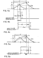
- Fig. 1 is a waveform of an input data signal in which pulsewidth is used to represent binary data as employed in the data receiver of the present invention;
- Fig. 2 is a schematic diagram of a portion of the data receiver of the present invention;
- Fig. 3 is a schematic diagram of the data-collection stage of the data receiver of the invention; .
- Fig. 4 a-c and Figs. 5 a and b are signal waveforms for use in describing the operation of the circuit of Fig. 2; and
- Figs. 6 a-e are waveforms of signals at several points in the data receiver of the invention.
- The self-clocking data receiver of the invention receives and processes data input signals in which the pulsewidths of the input pulses represent the two binary logic "1" and "0" levels, rather than the presence or absence of a pulse. An example of a data input signal in which pulsewidth is used to represent binary logic is provided in Fig. 1, in which a logic "0" is represented by a signal having a pulsewidth of T and a logic "1" is represented by a signal having a pulsewidth of 2T. It will be understood that the 2:1 ratio of the pulsewidths of the logic "1" and "0" signals shown in Fig. 1 is exemplary only, and that the data receiver of the invention as hereinafter described is also operable to receive and process signals having other pulse- width ratios to represent the binary states. It will also be noted in Fig. 1 that the period between a logic "0" and the following data signal is T, irrespective of the pulsewidth of the succeeding data signal, and that the period between a logic "1" signal and the succeeding data signal is 2T, again irrespective of the logic level of pulse- width of the succeeding data signal. This arrangement is also shown for exemplary purposes and also is not intended to limit the applicability or scope of the invention.
- The self-clocking data receiver of the invention, which receives a data input of the type illustrated in Fig. 1, is illustrated in Fig. 2. As therein shown, the data input is applied to an input
CMOS buffer gate 10 having an output node A. The output ofbuffer 10 is applied to the input of anintegration circuit 12, which may, as shown, consist of a variable resistor R connected to one plate of a capacitor C at a node B. The other plate of capacitor C.is connected to ground. - The output of the
integration circuit 12 at node B is connected to a resistor ladder circuit or voltage divider 14, which includes a pair of resistors R1 and R2 connected at a node C. The other end of resistor R1 is connected to node B, and the other end of resistor R2 is connected to' ground. Nodes B and C are respectively connected to the inputs ofCMOS buffer gates - As shown in Fig. 3, the clock signals at node D are applied to the D terminal of a D-type flip-
flop 20 and to the input of aninverter 22. The inverted clock output ofinverter 22 is applied to the clock input of an N-stage shift register 24, which stores bits Do, D1.....Dn, and to reset terminal of flip-flop 20. The data one signal at node E is applied to the C terminal of the flip-flop 20, and the Q terminal of the flip-flop is connected to the data in terminal ofshift register 24. - The operation of the circuit of Fig. 2 can be understood from the waveforms of Figs. 4, 5 and 6. Assuming a supply voltage of a level V applied to
CMOS gate buffer 10, as well as atCMOS buffers - Referring to Fig. 4a, when a square wave is applied to the
integration circuit 12, the voltage Vo at node B can be computed by: - At time T:

- At time 2T:

- Thus:

CMOS gates gate 16 is turned on and a clock pulse is produced at node D. The resistance value of resistor R inintegration circuit 12 can be adjusted such that the integrated voltage of node B exceeds 1/2 V0 for an input pulse of either pulsewidth T to T2, whereby a clock output at node D is-produced whenever a "0" or a "1" is presented at node A, as shown in Figs. 4b and 4e, respectively. - The pulsewidth of the clock output at node D is, however, different for a data "0" and a data "1" and can be calculated as follows:
- For a data "0" signal, charging to 1/2 V :


- Thus, Δ To = RC Ln2
- For data "0", discharging from V1 to 1/2 Vo;
- Thus,

- Therefore, the pulsewidth for a clock pulse produced for an input data "0" is, with reference to Fig. 4 (b) :

- Similarly, to compute the pulsewidth of a clock developed at node D in response to an input data "1" (Fig. 4(c)), to discharge from V2 to 1/2 Vo.


- Thus, ΔTone, the clock pulsewidth produced in response to a data "1" input, is:
- The pulsewidth of the clock outputs at node D produced for either a "0" or "1" input is thus independent of the supply voltage, such that any variation in the supply voltage will not affect the performance of the receiver.
- As noted previously, the integrated data signal at node B is also used to generate the data one signals in response to each input logic "1" data signal; that is, as shown in Fig. 1, all input signals having a pulse width of 2T. To this end, the ratio of resistors R1 and R2 in voltage divider 14 is selected such that the voltage at node C peaks at a level of 1/2 Vo (the CMOS gate switching level) when the voltage at node B peaks at voltage V1. In this case only a data "1" signal is able to pass through the data one
CMOS gate 18 to develop a data one signal (Fig. 6(e)) at node E. - With reference to Figs. 5 a and b, the ratio R1 necessary to achieve the desired voltage 1/2 V R2 at node C to develop a data one signal from each input logic "1" pulse of a pulsewidth 2T, can be calculated as follows:


- The voltage V2 at node C can be calculated as follows:

CMOS buffer gate 18, when the.voltage at node C reaches 1/2 Vo, the switching voltage ofgate 18, can be calculated as follows, with reference to Fig. 5b: - To discharge from V2 to 1/2 Vo


- It will be noted that the pulsewidth of the data one pulse is also independent of the supply voltage.
- Resistors R1 and R2 of the resistive voltage divider 14 have values of resistance that are an order of magnitude greater than that of the resistor R of
integration circuit 12, so that resistors R1 and R2 do not affect the charging and discharging of the integration circuit capacitor C. CMOS gates and buffers 10, 16, and 18 have very high input impedances on the charging and discharging of the integration circuit capacitor C. Moreover, the high resistance values of resistors R1 and R2 result in a reduction in the power dissipation in the circuit. - The temperature variation of the voltage ratio V21 that is the ratio of the integrated V1 voltages at node B for input pulses having pulse- widths of 2T and T, respectively, can be computed as follows:

- Since

- As noted, the self-synchronized data one and clock pulses produced at the outputs of
gates flop 20 is used to resolve the race condition of data input. At the leading edge of a data one signal, a data "1" clock pulse is loaded into the flip-flop 20. When a data "1" clock is presented, it stays in flip-flop 20 until a data one pulse is strobed intoshift register 24 at the trailing edge of the clock. The inactive state of the clock clears the flip-flop 20 and the flip-flop stays cleared if no data one is presented at its input. Thus, zero is strobed intoshift register 24 on the trailing edge of the clock pulse if a data "0" clock pulse is presented at the input of flip-flop 20. - Since the clock information is derived from the input data source, no synchronization is needed in the data receiver of the invention, which can thus receive the process data reliably under serious jitter conditions. Expensive stabilization circuits commonly used in binary data communication transmitters, computers, and radar systems, and in the servo speed control circuits used to drive magnetic discs and tapes and in rader systems thus become unnecessary. The data receiver system of the invention operates more reliably than the conventional data-clock synchronized receiver systems.
- It will be understood that whereas the present invention has been described hereinabove with respect to a single preferred embodiment, modifications may become apparent and made to the embodiment disclosed without necessarily departing from the spirit and scope of the invention.
Claims (5)
Applications Claiming Priority (2)
| Application Number | Priority Date | Filing Date | Title |
|---|---|---|---|
| US06/447,956 US4497060A (en) | 1982-12-08 | 1982-12-08 | Self-clocking binary receiver |
| US447956 | 1982-12-08 |
Publications (3)
| Publication Number | Publication Date |
|---|---|
| EP0112043A2 true EP0112043A2 (en) | 1984-06-27 |
| EP0112043A3 EP0112043A3 (en) | 1985-11-27 |
| EP0112043B1 EP0112043B1 (en) | 1988-04-20 |
Family
ID=23778430
Family Applications (1)
| Application Number | Title | Priority Date | Filing Date |
|---|---|---|---|
| EP83306906A Expired EP0112043B1 (en) | 1982-12-08 | 1983-11-11 | Self-clocking binary receiver |
Country Status (5)
| Country | Link |
|---|---|
| US (1) | US4497060A (en) |
| EP (1) | EP0112043B1 (en) |
| JP (1) | JPS59112747A (en) |
| CA (1) | CA1198780A (en) |
| DE (1) | DE3376376D1 (en) |
Cited By (3)
| Publication number | Priority date | Publication date | Assignee | Title |
|---|---|---|---|---|
| FR2606240A1 (en) * | 1986-11-05 | 1988-05-06 | Stc Plc | TRANSMITTER-RECEIVER FOR VERIFYING TRANSMISSION LINKS AND APPARATUS HAVING THE SAME |
| EP0387071A2 (en) * | 1989-03-09 | 1990-09-12 | Cotag International Limited | Codable electronic devices, e.g. transponders |
| EP0651538A1 (en) * | 1993-10-29 | 1995-05-03 | MAGNETI MARELLI S.p.A. | An interface for pulse width modulation communications |
Families Citing this family (40)
| Publication number | Priority date | Publication date | Assignee | Title |
|---|---|---|---|---|
| JPS60227547A (en) * | 1984-04-25 | 1985-11-12 | Mitsubishi Electric Corp | Digital remote controller |
| US4771440A (en) * | 1986-12-03 | 1988-09-13 | Cray Research, Inc. | Data modulation interface |
| US4817115A (en) * | 1987-02-27 | 1989-03-28 | Telxon Corporation | Encoding and decoding system for electronic data communication system |
| US4775804A (en) * | 1987-10-27 | 1988-10-04 | International Business Machines Corporation | Reconstructed clock generator |
| US5022052A (en) * | 1987-11-13 | 1991-06-04 | Seismograph Service Corp. | Analog signal binary transmission system using slope detection |
| US5930303A (en) * | 1996-11-04 | 1999-07-27 | Walker; Harold | Digital modulation employing single sideband with suppressed carrier |
| DE19647041A1 (en) * | 1996-11-14 | 1998-05-28 | Ziegler Horst | Process for the transmission of data |
| US5940135A (en) * | 1997-05-19 | 1999-08-17 | Aris Technologies, Inc. | Apparatus and method for encoding and decoding information in analog signals |
| US6427012B1 (en) * | 1997-05-19 | 2002-07-30 | Verance Corporation | Apparatus and method for embedding and extracting information in analog signals using replica modulation |
| US7644282B2 (en) | 1998-05-28 | 2010-01-05 | Verance Corporation | Pre-processed information embedding system |
| US6253332B1 (en) * | 1998-12-02 | 2001-06-26 | Sun Microsystems | Apparatus for generating shifted down clock signals |
| US6631165B1 (en) | 1999-09-01 | 2003-10-07 | Northrop Grumman Corporation | Code modulation using narrow spectral notching |
| US6737957B1 (en) | 2000-02-16 | 2004-05-18 | Verance Corporation | Remote control signaling using audio watermarks |
| US6512799B2 (en) * | 2001-02-06 | 2003-01-28 | University Of South Alabama | Digital communication system and method for increased bit rates |
| ES2507642T3 (en) | 2002-10-15 | 2014-10-15 | Verance Corporation | Media supervision, management and information system |
| US20060239501A1 (en) | 2005-04-26 | 2006-10-26 | Verance Corporation | Security enhancements of digital watermarks for multi-media content |
| US8020004B2 (en) | 2005-07-01 | 2011-09-13 | Verance Corporation | Forensic marking using a common customization function |
| US8781967B2 (en) * | 2005-07-07 | 2014-07-15 | Verance Corporation | Watermarking in an encrypted domain |
| US8566858B2 (en) * | 2005-09-20 | 2013-10-22 | Forefront Assets Limited Liability Company | Method, system and program product for broadcast error protection of content elements utilizing digital artifacts |
| US8566857B2 (en) * | 2005-09-20 | 2013-10-22 | Forefront Assets Limited Liability Company | Method, system and program product for broadcast advertising and other broadcast content performance verification utilizing digital artifacts |
| EP1927189B1 (en) * | 2005-09-20 | 2016-04-27 | Gula Consulting Limited Liability Company | Insertion and retrieval of identifying artifacts in transmitted lossy and lossless data |
| US8966517B2 (en) * | 2005-09-20 | 2015-02-24 | Forefront Assets Limited Liability Company | Method, system and program product for broadcast operations utilizing internet protocol and digital artifacts |
| EP2074518B1 (en) | 2006-09-27 | 2013-03-06 | Nxp B.V. | Spaced-one-hot receiver |
| US8259938B2 (en) * | 2008-06-24 | 2012-09-04 | Verance Corporation | Efficient and secure forensic marking in compressed |
| US8838977B2 (en) | 2010-09-16 | 2014-09-16 | Verance Corporation | Watermark extraction and content screening in a networked environment |
| US8615104B2 (en) | 2011-11-03 | 2013-12-24 | Verance Corporation | Watermark extraction based on tentative watermarks |
| US8923548B2 (en) | 2011-11-03 | 2014-12-30 | Verance Corporation | Extraction of embedded watermarks from a host content using a plurality of tentative watermarks |
| US8682026B2 (en) | 2011-11-03 | 2014-03-25 | Verance Corporation | Efficient extraction of embedded watermarks in the presence of host content distortions |
| US8533481B2 (en) | 2011-11-03 | 2013-09-10 | Verance Corporation | Extraction of embedded watermarks from a host content based on extrapolation techniques |
| US8745403B2 (en) | 2011-11-23 | 2014-06-03 | Verance Corporation | Enhanced content management based on watermark extraction records |
| US9323902B2 (en) | 2011-12-13 | 2016-04-26 | Verance Corporation | Conditional access using embedded watermarks |
| US9547753B2 (en) | 2011-12-13 | 2017-01-17 | Verance Corporation | Coordinated watermarking |
| US9571606B2 (en) | 2012-08-31 | 2017-02-14 | Verance Corporation | Social media viewing system |
| US8869222B2 (en) | 2012-09-13 | 2014-10-21 | Verance Corporation | Second screen content |
| US9106964B2 (en) | 2012-09-13 | 2015-08-11 | Verance Corporation | Enhanced content distribution using advertisements |
| US8726304B2 (en) | 2012-09-13 | 2014-05-13 | Verance Corporation | Time varying evaluation of multimedia content |
| US9262794B2 (en) | 2013-03-14 | 2016-02-16 | Verance Corporation | Transactional video marking system |
| US9251549B2 (en) | 2013-07-23 | 2016-02-02 | Verance Corporation | Watermark extractor enhancements based on payload ranking |
| US9208334B2 (en) | 2013-10-25 | 2015-12-08 | Verance Corporation | Content management using multiple abstraction layers |
| US9596521B2 (en) | 2014-03-13 | 2017-03-14 | Verance Corporation | Interactive content acquisition using embedded codes |
Citations (7)
| Publication number | Priority date | Publication date | Assignee | Title |
|---|---|---|---|---|
| US2616976A (en) * | 1947-03-05 | 1952-11-04 | Hartford Nat Bank & Trust Co | Multiplex radio receiver |
| US3281806A (en) * | 1962-12-21 | 1966-10-25 | Honeywell Inc | Pulse width modulation representation of paired binary digits |
| US3804982A (en) * | 1972-08-10 | 1974-04-16 | Texas Instruments Inc | Data communication system for serially transferring data between a first and a second location |
| US3991379A (en) * | 1975-06-03 | 1976-11-09 | United Technologies Corporation | Logic level decoding circuit |
| US4227181A (en) * | 1977-10-12 | 1980-10-07 | Ford Motor Company | Peripheral station in an information handling system |
| US4309664A (en) * | 1979-11-13 | 1982-01-05 | Gte Laboratories Incorporated | Digital energy line sensor |
| EP0059483A1 (en) * | 1981-03-04 | 1982-09-08 | Hermann Wangner GmbH & Co. KG | Shedding apparatus for the circular weaving of multi-harness fabrics and use of the shedding apparatus therefor |
Family Cites Families (2)
| Publication number | Priority date | Publication date | Assignee | Title |
|---|---|---|---|---|
| US3510780A (en) * | 1966-09-12 | 1970-05-05 | Motorola Inc | Two-state communication devices having combined clock and information signals |
| US3949199A (en) * | 1974-09-06 | 1976-04-06 | Avco Corporation | Pulse width decoder |
-
1982
- 1982-12-08 US US06/447,956 patent/US4497060A/en not_active Expired - Fee Related
-
1983
- 1983-11-08 CA CA000440639A patent/CA1198780A/en not_active Expired
- 1983-11-11 EP EP83306906A patent/EP0112043B1/en not_active Expired
- 1983-11-11 DE DE8383306906T patent/DE3376376D1/en not_active Expired
- 1983-11-26 JP JP58221461A patent/JPS59112747A/en active Pending
Patent Citations (7)
| Publication number | Priority date | Publication date | Assignee | Title |
|---|---|---|---|---|
| US2616976A (en) * | 1947-03-05 | 1952-11-04 | Hartford Nat Bank & Trust Co | Multiplex radio receiver |
| US3281806A (en) * | 1962-12-21 | 1966-10-25 | Honeywell Inc | Pulse width modulation representation of paired binary digits |
| US3804982A (en) * | 1972-08-10 | 1974-04-16 | Texas Instruments Inc | Data communication system for serially transferring data between a first and a second location |
| US3991379A (en) * | 1975-06-03 | 1976-11-09 | United Technologies Corporation | Logic level decoding circuit |
| US4227181A (en) * | 1977-10-12 | 1980-10-07 | Ford Motor Company | Peripheral station in an information handling system |
| US4309664A (en) * | 1979-11-13 | 1982-01-05 | Gte Laboratories Incorporated | Digital energy line sensor |
| EP0059483A1 (en) * | 1981-03-04 | 1982-09-08 | Hermann Wangner GmbH & Co. KG | Shedding apparatus for the circular weaving of multi-harness fabrics and use of the shedding apparatus therefor |
Non-Patent Citations (1)
| Title |
|---|
| E. H\LZLER et al.: "Theorie und Technik der Pulsmodulation", 1957, pages 439-440, chapter 6, section III.4, Springer-Verlag, Heidelberg, DE; * |
Cited By (4)
| Publication number | Priority date | Publication date | Assignee | Title |
|---|---|---|---|---|
| FR2606240A1 (en) * | 1986-11-05 | 1988-05-06 | Stc Plc | TRANSMITTER-RECEIVER FOR VERIFYING TRANSMISSION LINKS AND APPARATUS HAVING THE SAME |
| EP0387071A2 (en) * | 1989-03-09 | 1990-09-12 | Cotag International Limited | Codable electronic devices, e.g. transponders |
| EP0387071A3 (en) * | 1989-03-09 | 1993-07-07 | Cotag International Limited | Codable electronic devices, e.g. transponders |
| EP0651538A1 (en) * | 1993-10-29 | 1995-05-03 | MAGNETI MARELLI S.p.A. | An interface for pulse width modulation communications |
Also Published As
| Publication number | Publication date |
|---|---|
| US4497060A (en) | 1985-01-29 |
| EP0112043A3 (en) | 1985-11-27 |
| DE3376376D1 (en) | 1988-05-26 |
| JPS59112747A (en) | 1984-06-29 |
| CA1198780A (en) | 1985-12-31 |
| EP0112043B1 (en) | 1988-04-20 |
Similar Documents
| Publication | Publication Date | Title |
|---|---|---|
| EP0112043B1 (en) | Self-clocking binary receiver | |
| US4513427A (en) | Data and clock recovery system for data communication controller | |
| EP0679307B1 (en) | Delay line separator for data bus | |
| US6061418A (en) | Variable clock divider with selectable duty cycle | |
| US6424175B1 (en) | Biased control loop circuit for setting impedance of output driver | |
| US4529892A (en) | Detection circuitry with multiple overlapping thresholds | |
| US9240804B2 (en) | Techniques for alignment of parallel signals | |
| KR940017438A (en) | Integrated Waveshaping Circuit | |
| JPH0150150B2 (en) | ||
| EP0667533A2 (en) | Loss-of-signal detector | |
| US4611183A (en) | Digital decorrelating random data generator | |
| JPH06216778A (en) | Demodulation circuit for communication control equipment | |
| US4425514A (en) | Fixed pulse width, fast recovery one-shot pulse generator | |
| EP0237753A1 (en) | A frequency multiplier circuit | |
| JP3463727B2 (en) | Clock pulse transmission circuit | |
| US7505521B2 (en) | Data transmission system and method | |
| US5208831A (en) | Network interface system | |
| US4313107A (en) | Tone signal detectors | |
| JPH0936922A (en) | Digital signal modulating system | |
| US4780895A (en) | Circuit for stabilizing the rate at which pulses appear | |
| EP0777332A1 (en) | A Microwave multiphase detector | |
| US4644563A (en) | Data transmission method and system | |
| US6891402B2 (en) | Clock's out-of-synchronism state detection circuit and optical receiving device using the same | |
| US6550036B1 (en) | Pre-conditioner for measuring high-speed time intervals over a low-bandwidth path | |
| US5506533A (en) | Apparatus for generating a monostable signal |
Legal Events
| Date | Code | Title | Description |
|---|---|---|---|
| PUAI | Public reference made under article 153(3) epc to a published international application that has entered the european phase |
Free format text: ORIGINAL CODE: 0009012 |
|
| AK | Designated contracting states |
Designated state(s): DE FR GB |
|
| PUAL | Search report despatched |
Free format text: ORIGINAL CODE: 0009013 |
|
| AK | Designated contracting states |
Designated state(s): DE FR GB |
|
| 17P | Request for examination filed |
Effective date: 19860520 |
|
| 17Q | First examination report despatched |
Effective date: 19870612 |
|
| R17C | First examination report despatched (corrected) |
Effective date: 19870624 |
|
| GRAA | (expected) grant |
Free format text: ORIGINAL CODE: 0009210 |
|
| AK | Designated contracting states |
Kind code of ref document: B1 Designated state(s): DE FR GB |
|
| REF | Corresponds to: |
Ref document number: 3376376 Country of ref document: DE Date of ref document: 19880526 |
|
| ET | Fr: translation filed | ||
| PG25 | Lapsed in a contracting state [announced via postgrant information from national office to epo] |
Ref country code: GB Effective date: 19881111 |
|
| PLBE | No opposition filed within time limit |
Free format text: ORIGINAL CODE: 0009261 |
|
| STAA | Information on the status of an ep patent application or granted ep patent |
Free format text: STATUS: NO OPPOSITION FILED WITHIN TIME LIMIT |
|
| 26N | No opposition filed | ||
| GBPC | Gb: european patent ceased through non-payment of renewal fee | ||
| PG25 | Lapsed in a contracting state [announced via postgrant information from national office to epo] |
Ref country code: FR Free format text: LAPSE BECAUSE OF NON-PAYMENT OF DUE FEES Effective date: 19890731 |
|
| PG25 | Lapsed in a contracting state [announced via postgrant information from national office to epo] |
Ref country code: DE Effective date: 19890801 |
|
| REG | Reference to a national code |
Ref country code: FR Ref legal event code: ST |