EP0111128A2 - UV patterning of resist materials - Google Patents
UV patterning of resist materialsInfo
- Publication number
- EP0111128A2 EP0111128A2 EP83110676A EP83110676A EP0111128A2 EP 0111128 A2 EP0111128 A2 EP 0111128A2 EP 83110676 A EP83110676 A EP 83110676A EP 83110676 A EP83110676 A EP 83110676A EP 0111128 A2 EP0111128 A2 EP 0111128A2
- Authority
- EP
- European Patent Office
- Prior art keywords
- resist layer
- resist
- radiation
- layer
- substrate
- Prior art date
- Legal status (The legal status is an assumption and is not a legal conclusion. Google has not performed a legal analysis and makes no representation as to the accuracy of the status listed.)
- Withdrawn
Links
Images


Classifications
-
- H—ELECTRICITY
- H01—ELECTRIC ELEMENTS
- H01L—SEMICONDUCTOR DEVICES NOT COVERED BY CLASS H10
- H01L21/00—Processes or apparatus adapted for the manufacture or treatment of semiconductor or solid state devices or of parts thereof
- H01L21/02—Manufacture or treatment of semiconductor devices or of parts thereof
- H01L21/04—Manufacture or treatment of semiconductor devices or of parts thereof the devices having at least one potential-jump barrier or surface barrier, e.g. PN junction, depletion layer or carrier concentration layer
- H01L21/18—Manufacture or treatment of semiconductor devices or of parts thereof the devices having at least one potential-jump barrier or surface barrier, e.g. PN junction, depletion layer or carrier concentration layer the devices having semiconductor bodies comprising elements of Group IV of the Periodic System or AIIIBV compounds with or without impurities, e.g. doping materials
- H01L21/26—Bombardment with radiation
- H01L21/263—Bombardment with radiation with high-energy radiation
- H01L21/268—Bombardment with radiation with high-energy radiation using electromagnetic radiation, e.g. laser radiation
-
- G—PHYSICS
- G03—PHOTOGRAPHY; CINEMATOGRAPHY; ANALOGOUS TECHNIQUES USING WAVES OTHER THAN OPTICAL WAVES; ELECTROGRAPHY; HOLOGRAPHY
- G03F—PHOTOMECHANICAL PRODUCTION OF TEXTURED OR PATTERNED SURFACES, e.g. FOR PRINTING, FOR PROCESSING OF SEMICONDUCTOR DEVICES; MATERIALS THEREFOR; ORIGINALS THEREFOR; APPARATUS SPECIALLY ADAPTED THEREFOR
- G03F7/00—Photomechanical, e.g. photolithographic, production of textured or patterned surfaces, e.g. printing surfaces; Materials therefor, e.g. comprising photoresists; Apparatus specially adapted therefor
- G03F7/004—Photosensitive materials
- G03F7/039—Macromolecular compounds which are photodegradable, e.g. positive electron resists
-
- G—PHYSICS
- G03—PHOTOGRAPHY; CINEMATOGRAPHY; ANALOGOUS TECHNIQUES USING WAVES OTHER THAN OPTICAL WAVES; ELECTROGRAPHY; HOLOGRAPHY
- G03F—PHOTOMECHANICAL PRODUCTION OF TEXTURED OR PATTERNED SURFACES, e.g. FOR PRINTING, FOR PROCESSING OF SEMICONDUCTOR DEVICES; MATERIALS THEREFOR; ORIGINALS THEREFOR; APPARATUS SPECIALLY ADAPTED THEREFOR
- G03F7/00—Photomechanical, e.g. photolithographic, production of textured or patterned surfaces, e.g. printing surfaces; Materials therefor, e.g. comprising photoresists; Apparatus specially adapted therefor
- G03F7/20—Exposure; Apparatus therefor
- G03F7/2002—Exposure; Apparatus therefor with visible light or UV light, through an original having an opaque pattern on a transparent support, e.g. film printing, projection printing; by reflection of visible or UV light from an original such as a printed image
- G03F7/2004—Exposure; Apparatus therefor with visible light or UV light, through an original having an opaque pattern on a transparent support, e.g. film printing, projection printing; by reflection of visible or UV light from an original such as a printed image characterised by the use of a particular light source, e.g. fluorescent lamps or deep UV light
-
- H—ELECTRICITY
- H01—ELECTRIC ELEMENTS
- H01L—SEMICONDUCTOR DEVICES NOT COVERED BY CLASS H10
- H01L21/00—Processes or apparatus adapted for the manufacture or treatment of semiconductor or solid state devices or of parts thereof
- H01L21/02—Manufacture or treatment of semiconductor devices or of parts thereof
- H01L21/04—Manufacture or treatment of semiconductor devices or of parts thereof the devices having at least one potential-jump barrier or surface barrier, e.g. PN junction, depletion layer or carrier concentration layer
- H01L21/18—Manufacture or treatment of semiconductor devices or of parts thereof the devices having at least one potential-jump barrier or surface barrier, e.g. PN junction, depletion layer or carrier concentration layer the devices having semiconductor bodies comprising elements of Group IV of the Periodic System or AIIIBV compounds with or without impurities, e.g. doping materials
- H01L21/30—Treatment of semiconductor bodies using processes or apparatus not provided for in groups H01L21/20 - H01L21/26
- H01L21/31—Treatment of semiconductor bodies using processes or apparatus not provided for in groups H01L21/20 - H01L21/26 to form insulating layers thereon, e.g. for masking or by using photolithographic techniques; After treatment of these layers; Selection of materials for these layers
- H01L21/3105—After-treatment
- H01L21/311—Etching the insulating layers by chemical or physical means
- H01L21/31127—Etching organic layers
-
- H—ELECTRICITY
- H05—ELECTRIC TECHNIQUES NOT OTHERWISE PROVIDED FOR
- H05K—PRINTED CIRCUITS; CASINGS OR CONSTRUCTIONAL DETAILS OF ELECTRIC APPARATUS; MANUFACTURE OF ASSEMBLAGES OF ELECTRICAL COMPONENTS
- H05K3/00—Apparatus or processes for manufacturing printed circuits
- H05K3/0011—Working of insulating substrates or insulating layers
- H05K3/0017—Etching of the substrate by chemical or physical means
-
- Y—GENERAL TAGGING OF NEW TECHNOLOGICAL DEVELOPMENTS; GENERAL TAGGING OF CROSS-SECTIONAL TECHNOLOGIES SPANNING OVER SEVERAL SECTIONS OF THE IPC; TECHNICAL SUBJECTS COVERED BY FORMER USPC CROSS-REFERENCE ART COLLECTIONS [XRACs] AND DIGESTS
- Y10—TECHNICAL SUBJECTS COVERED BY FORMER USPC
- Y10S—TECHNICAL SUBJECTS COVERED BY FORMER USPC CROSS-REFERENCE ART COLLECTIONS [XRACs] AND DIGESTS
- Y10S430/00—Radiation imagery chemistry: process, composition, or product thereof
- Y10S430/146—Laser beam
-
- Y—GENERAL TAGGING OF NEW TECHNOLOGICAL DEVELOPMENTS; GENERAL TAGGING OF CROSS-SECTIONAL TECHNOLOGIES SPANNING OVER SEVERAL SECTIONS OF THE IPC; TECHNICAL SUBJECTS COVERED BY FORMER USPC CROSS-REFERENCE ART COLLECTIONS [XRACs] AND DIGESTS
- Y10—TECHNICAL SUBJECTS COVERED BY FORMER USPC
- Y10S—TECHNICAL SUBJECTS COVERED BY FORMER USPC CROSS-REFERENCE ART COLLECTIONS [XRACs] AND DIGESTS
- Y10S438/00—Semiconductor device manufacturing: process
- Y10S438/94—Laser ablative material removal
-
- Y—GENERAL TAGGING OF NEW TECHNOLOGICAL DEVELOPMENTS; GENERAL TAGGING OF CROSS-SECTIONAL TECHNOLOGIES SPANNING OVER SEVERAL SECTIONS OF THE IPC; TECHNICAL SUBJECTS COVERED BY FORMER USPC CROSS-REFERENCE ART COLLECTIONS [XRACs] AND DIGESTS
- Y10—TECHNICAL SUBJECTS COVERED BY FORMER USPC
- Y10S—TECHNICAL SUBJECTS COVERED BY FORMER USPC CROSS-REFERENCE ART COLLECTIONS [XRACs] AND DIGESTS
- Y10S438/00—Semiconductor device manufacturing: process
- Y10S438/942—Masking
- Y10S438/948—Radiation resist
- Y10S438/949—Energy beam treating radiation resist on semiconductor
Definitions
- the invention relates to a technique for patterning resist materials of the type used in lithographic processes, and more particularly to a technique for patterning these resists with extremely high efficiencies and rates of removal.
- resist layers comprised of organic materials are well known in the fabrication of microelectronic devices, and many different types of resists are available. These resists are designed to be sensitive to radiation of different wavelengths, including visible wavelengths, ultraviolet wavelengths, electron beams, and x-rays. In operation, the resists are exposed by incident radiation, and the exposed regions are either soluble (positive resist)or insoluble (negative resist) when developed later by a chemical solution. After development, a pattern is left in the resist layer, in accordance with the pattern of exposure.
- photoetching in accordance with this referenced article relies on an oxidative reaction.
- the incoming ultraviolet light photons are used to break bonds in the resist material, which is what any ultraviolet ray will do.
- oxygen enters and is absorbed in the polymer chains.
- the presence of oxygen is required to allow the bond-breaking process to continue and to produce oxidized species that can be removed.
- This is a process which is temperature dependent and which will slow down considerably as the system is cooled.
- any ultraviolet wavelength can be used, since the only purpose of the ultraviolet light is to break bonds so that oxygen can enter the fragmented polymer chains. Bond-breaks deep into the polymer are not required because the oxygen will not be able to diffuse into the depth of the polymer to oxidize the fragmented chains.
- any wavelength ultraviolet light can be used as long as oxygen is present.
- the etch rates are very slow, and certain resists (such as A.Z. 1350) cannot be photoetched by that process.
- the present invention is directed to a new and completely different mechanism which does not depend on the nature of the organic resist, on the presence of oxygen, or on temperature.
- the technique of this invention is critically dependent upon the wavelength of the applied radiation and on its power density (or energy fluence). It is termed “ablative photodecomposition” (APD), and requires high powered pulsed sources.
- organic resist materials of any type which are used in lithographic processes can be patterned by irradiation with ultraviolet radiation having wavelengths less than 220 nm and a power density at least as great as that which is necessary to cause ablative photodecomposition of the resist material.
- the radiation source must provide a sufficient number of photons in a short amount of time so that the resist polymer chains will be broken into fragments which ablate and are blown off as volatile by-products. This effect can occur in all resist materials and in a vacuum or other atmospheres, and is characterized by very large etch rates and a critical dependence on wavelength and power density.
- Pulsed radiation sources must be used, rather than continuous sources, in order to provide a sufficient amount of photons in the irradiated area of the resist in a very short amount of time.
- a particular example is pulsed laser radiation produced by an ArF excimer laser providing pulses approximately 10 nsec wide at 193 nm.
- the critical (threshold) energy fluence is approximately 10-15 mJ/cm2.
- Irradiation can proceed in a vacuum, or in a gaseous environment, including air and oxygen.
- the presence of oxygen is not required for ablative photodecomposition, but may make the process more efficient.
- the temperature of the organic resist is not material, room temperatures being suitable.
- the organic resists are those materials which are sensitive to incident radiation, where the resist is a material to be used in a lithographic process to produce devices and circuits.
- the invention therefore provides a fabrication process for producing a device or circuit, comprising depositing a resist layer on a substrate removing selected areas of the resist layer and causing a change to said exposed portions of said substrate through said removed areas of the resist layer, said process being characterised by removing the selected areas of said resist layer by irradiation of said selected areas with ultraviolet light of wavelengths less than 220 nm and having a sufficient power density to produce ablative photodecomposition of said irradiated areas to expose portions of said substrate.
- the invention also provides a method of forming a pattern in a layer of resist material of the typed used in lithography processes, said method comprising: depositing a layer of the resist material on a substrate, and irradiating selected areas of said resist layer with ultraviolet radiation having wavelengths less than 220 nm and an energy fluence in excess of that required to break polymer chains in said resist layer to produce enough broken fragments of said chains in a given time that said broken fragments will ablate and escape from said resist, leaving etched areas corresponding to the pattern of ultraviolet radiation incident on said resist layer.
- the present invention the patterning of resist layers of the type used in lithographic processes by ablative photodecomposition.
- FIG. 1.1 - 1.3 illustrate this mechanism.
- a resist layer 10 is schematically illustrated by a group of horizontal lines 11, representing polymer chains in the resist layer.
- Far UV light of wavelengths less than 220 nm and sufficiently high power density to cause ablative photodecomposition, represented by the arrows 12, is directed toward resist layer 10.
- a mask 14 is used to define the areas of resist 10 which are to be irradiated by the ultraviolet radiation. This is the light absorption part of ablative photodecomposition, where the absorption of incoming photons is confined to a thin surface 0 layer, typically less than 3000A. Generally, about 95% of the input photons are absorbed in the first 2700 angstroms of the resist layer 10.
- FIG. 1.2 represents the second step in the ablative photodecomposition process. This is termed bond-breaking, in which the incoming photons break the long polymer chains 11 in resist layer 10. This is indicated by the small broken fragments 16 in those areas where the radiation strikes resist 10.
- the quantum yield for bond-breaking at wavelengths less than 220 nm is very high, typically 750% for radiation at 193 nm.
- the third step, ablation, is illustrated in FIG. 1.3.
- Ablation occurs when the fluence of the laser pulse exceeds a threshold value (- mJ/cm2), and is caused by an increase in pressure when small fragments 16 replace the long chains 11 in the resist layer.
- the small fragments 16 are produced in a very short amount of time in a small volume, and require more volume than the long, unbroken chains.
- This sudden buildup in pressure causes ablation, in which the fragments 16 explosively burst out of the irradiation volume, leaving ablatively photodecomposed regions 18.
- the energy of the photons exceeds the dissociation energy of any of the bonds in the organic resist molecules, and the excess energy is carried away by the fragments.
- the area of removal of the resist material by APD is completely defined by the light, and the remaining resist is not heated. In this process, the presence of a gaseous atmosphere is not required, but oxidation in air will promote the reaction and increase its efficiency.
- Ablative photodecomposition requires that a large number of fragments 16 be created in the irradiated volume of the resist layer 10 in a short amount of time.
- This requires pulsed radiation of the type produced by a laser, such as the ArF excimer laser which produces ultraviolet radiation at 193 nm.
- These lasers provide pulsed outputs of about 10-15 nsec width, and can provide 10-100 pulses per second.
- the energy fluence of these pulses is typically in excess of 10 mJ/cm .
- FIG. 2 shows an apparatus which is suitable to carry out ablative photodecomposition.
- the apparatus is comprised of a vacuum chamber 20 having an input port 22 through which gases, including air, can be admitted, as indicated by arrow 24.
- Chamber 20 is provided with an output port 26 to which a pump 28 is attached for removing volatile by-products and gases from chamber 20 as indicated by arrow 30.
- a quartz window 32 allows ultraviolet radiation 34 to enter chamber 20. This radiation is provided by the far-UV source 36, which produces radiation of wavelengths less than 220 nm and of sufficient power density to produce ablative photodecomposition.
- resist layer 38 Located within chamber 20 are the resist layer 38 to be patterned, and the substrate 40 on which resist layer 38 is ' ' located.
- Substrate 40 can be comprised of a multitude of layers including metals, insulators, and semiconductors.
- Resist layer 38 is typically present to provide a mask for the patterning of underlying layers, or for selective deposition of another layer, etc., as is well known in lithographic processes. If desired, a mask 42 is used to define the areas of resist layer 38 to be irradiated.
- the source 36 is typically a laser source which will provide a sufficient number of photons of at least a threshold energy fluence in a very short amount of time, the amount of energy and the period of time being chosen to be sufficient to ablatively photodecompose the irradiated areas of layer 38.
- a suitable laser is the ArF excimer laser providing a pulsed output at 193 nm.
- the laser source must provide a sufficient amount of energy in a short amount of time in order to cause ablative photodecomposition.
- ArF laser pulses 12 nsec wide it has been found that an energy fluence of 7.5 mJ/cm 2 /pulse is not sufficient to ablatively photodecompose the resist, while energy fluences of 15 mJ/cm 2 /pulse are sufficient.
- a threshold appears to be between these two energy fluences and is probably about 10-12 mJ/cm /pulse.
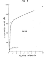
- FIG. 3 is a plot of the etch rate per pulse plotted against the relative intensity of the input laser pulse, when PMMA is ablatively photodecomposed.
- the highly nonlinear nature of ablative photodecomposition is readily apparent from FIG. 3. This contrasts greatly with the more linear etch rates which are obtained using oxidative removal as the etching mechanism.
- the etch rate/pulse increases greatly once a threshold of intensity is reached. Extremely high etch rates can be obtained having magnitudes which can. never be obtained with oxidative removal processes.
- FIGS. 4.1 - 4.3 illustrate a particular use for this invention, where a single layer of negative resist is used to provide different patterns.
- a negative resist layer 44 is located on a substrate 46.
- Substrate 46 can be comprised of multilayers of films of all types, including insulators, metals, and semiconductors.
- negative resist 44 has been patterned in a conventional way, including exposure to long wavelength radiation of the magnitude typically used in the art to produce crosslinking of the polymer chains where the radiation strikes resist layer 44. These irradiated regions become insoluble when a development solution is applied to the resist. Thus, this is a negative resist because the portions remaining after development are those portions which were not exposed to the incident light.
- a subsequent fabrication step such as an etching, doping, etc. of substrate 46, can be undertaken.
- the same resist pattern remains on the substrate 46.
- short wavelengths of ultraviolet radiation 48 having wavelengths less than 220 nm is used to ablatively photodecompose portions of the resist layer 44. Those portions to be irradiated are determined by the mask 50.
- the ablative photodecomposition will cause removal of the resist layer where it is irradiated to yield the pattern shown in FIG. 4.3.
- portions of the resist layer which are irradiated are removed and the negative resist becomes a "positive" resist. In this manner, a new pattern is provided for subsequent processing of substrate 46.
- the practice of this invention is primarily directed to ablative photodecomposition of resist materials, either positive or negative, and particularly the use of this technique for device and circuit fabrication. Any type of resist material can be ablatively photodecomposed, but the invention is limited to resist materials which will be used in lithography. Thus, in the process described by FIGS. 4.1 - 4.3, the next step would be the removal of resist layer 44 and the continuance of the device or circuit fabrication process. These additional steps include the deposition of subsequent layers or the etching of existing layers, where resists are required to be patterned for either additive or substractive steps in the process.
- KPR Kodak photoresists
- KTFR thin photoresists
- KOR orthoresists
- resist layers are patterned to define a subsequent fabrication step, including modification of an underlying layer as by doping, addition of another layer, or subtraction of an underlying layer.
- the nature of the layer to be affected through the ablatively photodecomposed resist layer can be any material, including insulators, metals, and semiconductors.
Abstract
Description
- The invention relates to a technique for patterning resist materials of the type used in lithographic processes, and more particularly to a technique for patterning these resists with extremely high efficiencies and rates of removal.
- The use of resist layers comprised of organic materials is well known in the fabrication of microelectronic devices, and many different types of resists are available. These resists are designed to be sensitive to radiation of different wavelengths, including visible wavelengths, ultraviolet wavelengths, electron beams, and x-rays. In operation, the resists are exposed by incident radiation, and the exposed regions are either soluble (positive resist)or insoluble (negative resist) when developed later by a chemical solution. After development, a pattern is left in the resist layer, in accordance with the pattern of exposure.
- The resolution obtainable in producing patterns depends inversely upon the wavelength used to expose the resist. For this reason, organic resists sensitive to short wavelength radiation, such as ultraviolet radiation, electron beams, and x-rays, have been developed.
- In the prior art, there have been attempts to eliminate the development steps, and these have had some mixed degree of success. For example, reference is made to an article by Ueno et al, entitled "Direct Etching of Resists by UV Light", which appeared in the Japanese Journal of Applied Physics, Vol. 20, No. 10, October 1981, at pages L709-L712. In this article, the authors describe dry etching of photoresists by ultraviolet light having wavelengths 180-290 nm. The process by which dry etching occurs is an oxidative process which will not proceed in the absence of an oxygen environment. The authors therein used 180 nm ultraviolet light from a stationary deuterium discharge lamp having a power of approximately 8 mJ/cm2. Photoetching was observed, but the etching rates were quite slow, and oxygen was needed in the etching environment. In the case of AZ-1350 resist (produced by the Shipley Corporation), no etching was observed even after irradiation for more than 100 minutes.
- As noted, photoetching in accordance with this referenced article relies on an oxidative reaction. The incoming ultraviolet light photons are used to break bonds in the resist material, which is what any ultraviolet ray will do. After the bonds are broken, oxygen enters and is absorbed in the polymer chains. The presence of oxygen is required to allow the bond-breaking process to continue and to produce oxidized species that can be removed. This is a process which is temperature dependent and which will slow down considerably as the system is cooled. 'It is also a process which does not have a strict dependence on the wavelength of the light which is used. In fact, any ultraviolet wavelength can be used, since the only purpose of the ultraviolet light is to break bonds so that oxygen can enter the fragmented polymer chains. Bond-breaks deep into the polymer are not required because the oxygen will not be able to diffuse into the depth of the polymer to oxidize the fragmented chains. Thus, in the process of that reference, any wavelength ultraviolet light can be used as long as oxygen is present.
- In that reference, the etch rates are very slow, and certain resists (such as A.Z. 1350) cannot be photoetched by that process.
- In contrast to the techniques of the prior art using oxidative removal, the present invention is directed to a new and completely different mechanism which does not depend on the nature of the organic resist, on the presence of oxygen, or on temperature. In further contrast with the technique of oxidative removal, the technique of this invention is critically dependent upon the wavelength of the applied radiation and on its power density (or energy fluence). It is termed "ablative photodecomposition" (APD), and requires high powered pulsed sources.
- In APD, a large number of photons of a particular .wavelength are directed to the resist material in a short time. The efficiency for absorption of these photons is very high, and many polymer chain fragments are produced in a small volume in a very short amount of time. This causes a localized increase in volume which cannot be sustained, and the pressure is relieved by the process of ablation, wherein fragmented chains explode and escape from the resist, leaving an etched material. In this process, a rapid and large amount of bond-breaking must occur at the surface of the resist in order to allow the fragmented by-products to explode and escape from the surface of the resist. The process is such that the incident energy is transferred to kinetic energy of the ablated by-products. Ablative photodecomposition leads to extremely high etch rates, being at least 30 times as great as those obtainable in oxidative removal processes.
- Accordingly, it is a primary object of the present invention to provide a new technique for etching resist . materials by applied radiation, without requiring a development step.
- It is another object of this invention to provide a technique for etching resist materials with high efficiency.
- It is another object of this invention to provide a technique for etching resist materials wherein very high rates of removal are obtained, without the necessity of a development step.
- It is another object of the present invention to provide a technique using irradiation for etching all types of resist.
- It is yet another object of the present invention to provide a technique for etching all types of organic resist material without the need for a particular type of gaseous environment.
- It is a further object of this invention to provide a technique for etching all types of resist materials, in which temperature is not critical.
- It is a still further object of this invention to provide a technique for etching organic resist materials by a new mechanism having extremely high efficiency.
- It is another object of the present invention to provide a technique for etching organic resist materials to produce fine line patterns therein wherein said technique can be readily applied to practical processes or device fabrications, and which does not require subsequent development steps.
- It is another object ot the present invention to provide a dry etch process for selectively removing portions of an organic resist layer which can be used to etch any type of organic resist material in any atmosphere or in vacuum, and at any temperature.
- In the practice of this invention, organic resist materials of any type which are used in lithographic processes can be patterned by irradiation with ultraviolet radiation having wavelengths less than 220 nm and a power density at least as great as that which is necessary to cause ablative photodecomposition of the resist material.
- That is, the radiation source must provide a sufficient number of photons in a short amount of time so that the resist polymer chains will be broken into fragments which ablate and are blown off as volatile by-products. This effect can occur in all resist materials and in a vacuum or other atmospheres, and is characterized by very large etch rates and a critical dependence on wavelength and power density.
- Pulsed radiation sources must be used, rather than continuous sources, in order to provide a sufficient amount of photons in the irradiated area of the resist in a very short amount of time. A particular example is pulsed laser radiation produced by an ArF excimer laser providing pulses approximately 10 nsec wide at 193 nm. The critical (threshold) energy fluence is approximately 10-15 mJ/cm2.
- Irradiation can proceed in a vacuum, or in a gaseous environment, including air and oxygen. The presence of oxygen is not required for ablative photodecomposition, but may make the process more efficient. The temperature of the organic resist is not material, room temperatures being suitable.
- In the practice of this invention, the organic resists are those materials which are sensitive to incident radiation, where the resist is a material to be used in a lithographic process to produce devices and circuits.
- The invention therefore provides a fabrication process for producing a device or circuit, comprising depositing a resist layer on a substrate removing selected areas of the resist layer and causing a change to said exposed portions of said substrate through said removed areas of the resist layer, said process being characterised by removing the selected areas of said resist layer by irradiation of said selected areas with ultraviolet light of wavelengths less than 220 nm and having a sufficient power density to produce ablative photodecomposition of said irradiated areas to expose portions of said substrate.
- The invention also provides a method of forming a pattern in a layer of resist material of the typed used in lithography processes, said method comprising: depositing a layer of the resist material on a substrate, and irradiating selected areas of said resist layer with ultraviolet radiation having wavelengths less than 220 nm and an energy fluence in excess of that required to break polymer chains in said resist layer to produce enough broken fragments of said chains in a given time that said broken fragments will ablate and escape from said resist, leaving etched areas corresponding to the pattern of ultraviolet radiation incident on said resist layer.
- The invention will now be further described with reference to the accompanying drawings, in which:-
- FIGS. 1.1 - 1.3 schematically illustrate the process of ablative photodecomposition.
- FIG. 2 schematically illustrates an apparatus suitable for carrying out the present invention.
- FIG. 3 is a plot of etch rate/pulse versus relative intensity of the input radiation for ablative photodecomposition of poly (methylmethacrylate-PMMA) resist, using 193 nm laser radiation from a pulsed ArF laser.
- FIGS. 4.1 - 4.3 illustrate the use of ablative photodecomposition to pattern for a second time a negative resist layer which has been patterned by conventional techniques.
- The present invention the patterning of resist layers of the type used in lithographic processes by ablative photodecomposition. FIG. 1.1 - 1.3 illustrate this mechanism.
- In FIG. 1.1, a resist
layer 10 is schematically illustrated by a group of horizontal lines 11, representing polymer chains in the resist layer. Far UV light of wavelengths less than 220 nm and sufficiently high power density to cause ablative photodecomposition, represented by thearrows 12, is directed toward resistlayer 10. Amask 14 is used to define the areas of resist 10 which are to be irradiated by the ultraviolet radiation. This is the light absorption part of ablative photodecomposition, where the absorption of incoming photons is confined to athin surface 0 layer, typically less than 3000A. Generally, about 95% of the input photons are absorbed in the first 2700 angstroms of the resistlayer 10. - FIG. 1.2 represents the second step in the ablative photodecomposition process. This is termed bond-breaking, in which the incoming photons break the long polymer chains 11 in resist
layer 10. This is indicated by the smallbroken fragments 16 in those areas where the radiation strikes resist 10. The quantum yield for bond-breaking at wavelengths less than 220 nm is very high, typically 750% for radiation at 193 nm. - The third step, ablation, is illustrated in FIG. 1.3. Ablation occurs when the fluence of the laser pulse exceeds a threshold value (- mJ/cm2), and is caused by an increase in pressure when
small fragments 16 replace the long chains 11 in the resist layer. Thesmall fragments 16 are produced in a very short amount of time in a small volume, and require more volume than the long, unbroken chains. This sudden buildup in pressure causes ablation, in which thefragments 16 explosively burst out of the irradiation volume, leaving ablativelyphotodecomposed regions 18. The energy of the photons exceeds the dissociation energy of any of the bonds in the organic resist molecules, and the excess energy is carried away by the fragments. The area of removal of the resist material by APD is completely defined by the light, and the remaining resist is not heated. In this process, the presence of a gaseous atmosphere is not required, but oxidation in air will promote the reaction and increase its efficiency. - Ablative photodecomposition requires that a large number of
fragments 16 be created in the irradiated volume of the resistlayer 10 in a short amount of time. This requires pulsed radiation of the type produced by a laser, such as the ArF excimer laser which produces ultraviolet radiation at 193 nm. These lasers provide pulsed outputs of about 10-15 nsec width, and can provide 10-100 pulses per second. The energy fluence of these pulses is typically in excess of 10 mJ/cm . - While a representative example using the ArF laser is given, it should be understood that the amount of power density required in the input pulse, and the time in which the bond-breaking must occur, will depend to some degree on the nature of the resist layer. It has been found that photoresist layers of the type commercially available can be ablatively photodecomposed by pulsed 193 nm radiation from the ArF excimer laser.
- As has been noted, a large amount of energy, greater than a threshold amount, must be applied before ablation will occur. Energies and power densities of this magnitude are usually available only from lasers. Interestingly, the time integrals of applied energy, from both a laser and a stationary lamp, are often the same in terms of total power; however, the input energy must be sufficiently great and must be applied in a very short amount of time in order to produce ablative photodecomposition. This is why lasers are effective for APD presently available, and stationary lamps are not.
- FIG. 2 shows an apparatus which is suitable to carry out ablative photodecomposition. The apparatus is comprised of a
vacuum chamber 20 having aninput port 22 through which gases, including air, can be admitted, as indicated byarrow 24.Chamber 20 is provided with anoutput port 26 to which apump 28 is attached for removing volatile by-products and gases fromchamber 20 as indicated byarrow 30. Aquartz window 32 allowsultraviolet radiation 34 to enterchamber 20. This radiation is provided by the far-UV source 36, which produces radiation of wavelengths less than 220 nm and of sufficient power density to produce ablative photodecomposition. - Located within
chamber 20 are the resistlayer 38 to be patterned, and thesubstrate 40 on which resistlayer 38 is ' 'located.Substrate 40 can be comprised of a multitude of layers including metals, insulators, and semiconductors. Resistlayer 38 is typically present to provide a mask for the patterning of underlying layers, or for selective deposition of another layer, etc., as is well known in lithographic processes. If desired, amask 42 is used to define the areas of resistlayer 38 to be irradiated. - As was noted, the
source 36 is typically a laser source which will provide a sufficient number of photons of at least a threshold energy fluence in a very short amount of time, the amount of energy and the period of time being chosen to be sufficient to ablatively photodecompose the irradiated areas oflayer 38. A suitable laser is the ArF excimer laser providing a pulsed output at 193 nm. - It has been mentioned that the laser source must provide a sufficient amount of energy in a short amount of time in order to cause ablative photodecomposition. For commercially available resists irradiated by
ArF laser pulses 12 nsec wide, it has been found that an energy fluence of 7.5 mJ/cm2/pulse is not sufficient to ablatively photodecompose the resist, while energy fluences of 15 mJ/cm2/pulse are sufficient. A threshold appears to be between these two energy fluences and is probably about 10-12 mJ/cm /pulse. - FIG. 3 is a plot of the etch rate per pulse plotted against the relative intensity of the input laser pulse, when PMMA is ablatively photodecomposed. The highly nonlinear nature of ablative photodecomposition is readily apparent from FIG. 3. This contrasts greatly with the more linear etch rates which are obtained using oxidative removal as the etching mechanism. The etch rate/pulse increases greatly once a threshold of intensity is reached. Extremely high etch rates can be obtained having magnitudes which can. never be obtained with oxidative removal processes.
- FIGS. 4.1 - 4.3 illustrate a particular use for this invention, where a single layer of negative resist is used to provide different patterns.
- In FIG. 4.1, a negative resist
layer 44 is located on asubstrate 46.Substrate 46 can be comprised of multilayers of films of all types, including insulators, metals, and semiconductors. In this this film fabrication technique, it is desired to pattern a layer located under negative resist 44. Accordingly, in FIG. 4.1, negative resist 44 has been patterned in a conventional way, including exposure to long wavelength radiation of the magnitude typically used in the art to produce crosslinking of the polymer chains where the radiation strikes resistlayer 44. These irradiated regions become insoluble when a development solution is applied to the resist. Thus, this is a negative resist because the portions remaining after development are those portions which were not exposed to the incident light. Using this resist pattern, a subsequent fabrication step, such as an etching, doping, etc. ofsubstrate 46, can be undertaken. - In FIG. 4.2, the same resist pattern remains on the
substrate 46. At this time, short wavelengths ofultraviolet radiation 48 having wavelengths less than 220 nm is used to ablatively photodecompose portions of the resistlayer 44. Those portions to be irradiated are determined by themask 50. The ablative photodecomposition will cause removal of the resist layer where it is irradiated to yield the pattern shown in FIG. 4.3. In the ablative photodecomposition step, portions of the resist layer which are irradiated are removed and the negative resist becomes a "positive" resist. In this manner, a new pattern is provided for subsequent processing ofsubstrate 46. - The practice of this invention is primarily directed to ablative photodecomposition of resist materials, either positive or negative, and particularly the use of this technique for device and circuit fabrication. Any type of resist material can be ablatively photodecomposed, but the invention is limited to resist materials which will be used in lithography. Thus, in the process described by FIGS. 4.1 - 4.3, the next step would be the removal of resist
layer 44 and the continuance of the device or circuit fabrication process. These additional steps include the deposition of subsequent layers or the etching of existing layers, where resists are required to be patterned for either additive or substractive steps in the process. - While all types of resist materials can be patterned by APD, the invention is particularly suited to the patterning of photoresists. Included among the many resists which can be patterned are Kodak photoresists (KPR), thin photoresists (KTFR), and orthoresists (KOR), all of which are produced by the Kodak Company, Rochester, New York. The AZ series of resists produced by the Shipley Company, the RISTON resists (a trademark of E. I. DuPont de Nemours Company), and resists produced by the Hunt Chemical Company.
- Thus, in the practice of this invention an improved device and circuit fabrication process is described in which resist layers are patterned to define a subsequent fabrication step, including modification of an underlying layer as by doping, addition of another layer, or subtraction of an underlying layer. The nature of the layer to be affected through the ablatively photodecomposed resist layer can be any material, including insulators, metals, and semiconductors.
- While the invention has been described with respect to particular embodiments thereof, it will be understood by those of skill in the art that variations may be made therein without departing from the scope of the claimed invention.
Claims (9)
Applications Claiming Priority (2)
| Application Number | Priority Date | Filing Date | Title |
|---|---|---|---|
| US06/448,126 US4414059A (en) | 1982-12-09 | 1982-12-09 | Far UV patterning of resist materials |
| US448126 | 1982-12-09 |
Publications (2)
| Publication Number | Publication Date |
|---|---|
| EP0111128A2 true EP0111128A2 (en) | 1984-06-20 |
| EP0111128A3 EP0111128A3 (en) | 1984-08-01 |
Family
ID=23779107
Family Applications (1)
| Application Number | Title | Priority Date | Filing Date |
|---|---|---|---|
| EP83110676A Withdrawn EP0111128A3 (en) | 1982-12-09 | 1983-10-26 | Uv patterning of resist materials |
Country Status (3)
| Country | Link |
|---|---|
| US (1) | US4414059A (en) |
| EP (1) | EP0111128A3 (en) |
| JP (1) | JPS59105638A (en) |
Cited By (14)
| Publication number | Priority date | Publication date | Assignee | Title |
|---|---|---|---|---|
| WO1986000427A1 (en) * | 1984-06-21 | 1986-01-16 | American Telephone & Telegraph Company | Deep-uv lithography |
| WO1988002550A1 (en) * | 1986-09-26 | 1988-04-07 | General Electric Company | Method to produce via holes in polymer dielectrics for multiple electronic circuit chip packaging |
| EP0272799A1 (en) * | 1986-11-26 | 1988-06-29 | Quick Technologies Ltd. | Ablative etch resistant coating for laser personalization of integrated circuits |
| US4783695A (en) * | 1986-09-26 | 1988-11-08 | General Electric Company | Multichip integrated circuit packaging configuration and method |
| DE3835636A1 (en) * | 1987-10-23 | 1989-05-03 | Galram Technology Ind Ltd | METHOD AND SYSTEM FOR COMPLETELY REMOVING PHOTORESIST |
| EP0315152A2 (en) * | 1987-11-03 | 1989-05-10 | AUSIMONT S.r.l. | Photoablation process for films based on polymers having a perfluoroalkylpolyether structure by means of excimer laser rays |
| US4835704A (en) * | 1986-12-29 | 1989-05-30 | General Electric Company | Adaptive lithography system to provide high density interconnect |
| US4866508A (en) * | 1986-09-26 | 1989-09-12 | General Electric Company | Integrated circuit packaging configuration for rapid customized design and unique test capability |
| US4875971A (en) * | 1987-04-05 | 1989-10-24 | Elron Electronic Industries, Ltd. | Fabrication of customized integrated circuits |
| US4924287A (en) * | 1985-01-20 | 1990-05-08 | Avner Pdahtzur | Personalizable CMOS gate array device and technique |
| US4937203A (en) * | 1986-09-26 | 1990-06-26 | General Electric Company | Method and configuration for testing electronic circuits and integrated circuit chips using a removable overlay layer |
| US5094709A (en) * | 1986-09-26 | 1992-03-10 | General Electric Company | Apparatus for packaging integrated circuit chips employing a polymer film overlay layer |
| EP0502632A1 (en) * | 1991-03-07 | 1992-09-09 | Minnesota Mining And Manufacturing Company | Process for producing a patterned metal surface |
| WO2005094147A1 (en) * | 2004-03-25 | 2005-10-06 | Dsm Ip Assets B.V. | A process of forming a solder mask |
Families Citing this family (146)
| Publication number | Priority date | Publication date | Assignee | Title |
|---|---|---|---|---|
| JPS58146040A (en) * | 1982-02-24 | 1983-08-31 | Pioneer Video Kk | Optical system information recording original disk |
| US4568632A (en) * | 1982-10-07 | 1986-02-04 | International Business Machines Corporation | Patterning of polyimide films with far ultraviolet light |
| JPS60124393A (en) * | 1983-12-09 | 1985-07-03 | 日産自動車株式会社 | Method of producing polycolor light emitting thin film el panel |
| US4507331A (en) * | 1983-12-12 | 1985-03-26 | International Business Machines Corporation | Dry process for forming positive tone micro patterns |
| EP0152766A1 (en) * | 1984-01-24 | 1985-08-28 | Shiley Incorporated | Reduction of an arteriosclerotic lesion by selective absorption of electromagnetic energy in a component thereof |
| US4588801A (en) | 1984-04-05 | 1986-05-13 | The United States Of America As Represented By The United States Department Of Energy | Polysilane positive photoresist materials and methods for their use |
| EP0164564A1 (en) * | 1984-05-18 | 1985-12-18 | Siemens Aktiengesellschaft | Arrangement for the production of blind holes in a laminated construction |
| JPS61108195A (en) * | 1984-11-01 | 1986-05-26 | インタ−ナショナル ビジネス マシ−ンズ コ−ポレ−ション | Formation of electrically continued layers on substrate |
| US4643799A (en) * | 1984-12-26 | 1987-02-17 | Hitachi, Ltd. | Method of dry etching |
| US4652721A (en) * | 1985-01-03 | 1987-03-24 | Dow Corning Corporation | Method and apparatus for edge contouring lenses |
| JPS61187237A (en) * | 1985-02-14 | 1986-08-20 | Toshiba Corp | Formation of pattern |
| JPS62160981A (en) * | 1986-01-08 | 1987-07-16 | Mitsubishi Heavy Ind Ltd | Reconstruction method for oil tanker |
| US4704342A (en) * | 1985-04-02 | 1987-11-03 | Fairchild Semiconductor Corporation | Photomask having a patterned carbon light-blocking coating |
| US4617085A (en) * | 1985-09-03 | 1986-10-14 | General Electric Company | Process for removing organic material in a patterned manner from an organic film |
| US4648936A (en) * | 1985-10-11 | 1987-03-10 | The United States Of America As Represented By The United States Department Of Energy | Dopant type and/or concentration selective dry photochemical etching of semiconductor materials |
| US4684437A (en) * | 1985-10-31 | 1987-08-04 | International Business Machines Corporation | Selective metal etching in metal/polymer structures |
| US4735885A (en) * | 1985-12-06 | 1988-04-05 | Allied Corporation | Deep UV photoresist composition with 1,3-disubstituted-5-diazobarbituric acids |
| EP0233755B1 (en) * | 1986-02-14 | 1991-02-06 | Amoco Corporation | Ultraviolet laser treating of molded surfaces |
| US4856513A (en) * | 1987-03-09 | 1989-08-15 | Summit Technology, Inc. | Laser reprofiling systems and methods |
| GB8606821D0 (en) | 1986-03-19 | 1986-04-23 | Pa Consulting Services | Corneal reprofiling |
| US4748103A (en) * | 1986-03-21 | 1988-05-31 | Advanced Power Technology | Mask-surrogate semiconductor process employing dopant protective region |
| US4752668A (en) * | 1986-04-28 | 1988-06-21 | Rosenfield Michael G | System for laser removal of excess material from a semiconductor wafer |
| IT1196447B (en) * | 1986-07-03 | 1988-11-16 | Montedison Spa | PHOTOABLATION PROCESS OF SURFACE COATINGS BASED ON POLYMERIC MATERIAL |
| US5064681A (en) * | 1986-08-21 | 1991-11-12 | International Business Machines Corporation | Selective deposition process for physical vapor deposition |
| DE3770896D1 (en) * | 1986-09-15 | 1991-07-25 | Gen Electric | METHOD FOR PHOTOSELECTIVE METALIZATION. |
| US4865873A (en) * | 1986-09-15 | 1989-09-12 | General Electric Company | Electroless deposition employing laser-patterned masking layer |
| US5053171A (en) * | 1986-10-14 | 1991-10-01 | Allergan, Inc. | Manufacture of ophthalmic lenses by excimer laser |
| US5061840A (en) * | 1986-10-14 | 1991-10-29 | Allergan, Inc. | Manufacture of ophthalmic lenses by excimer laser |
| US5179262A (en) * | 1986-10-14 | 1993-01-12 | Allergan, Inc. | Manufacture of ophthalmic lenses by excimer laser |
| US4842782A (en) * | 1986-10-14 | 1989-06-27 | Allergan, Inc. | Manufacture of ophthalmic lenses by excimer laser |
| US4816422A (en) * | 1986-12-29 | 1989-03-28 | General Electric Company | Fabrication of large power semiconductor composite by wafer interconnection of individual devices |
| US4801352A (en) * | 1986-12-30 | 1989-01-31 | Image Micro Systems, Inc. | Flowing gas seal enclosure for processing workpiece surface with controlled gas environment and intense laser irradiation |
| US4718974A (en) * | 1987-01-09 | 1988-01-12 | Ultraphase Equipment, Inc. | Photoresist stripping apparatus using microwave pumped ultraviolet lamp |
| US5032209A (en) * | 1987-03-16 | 1991-07-16 | Minnesota Mining And Manufacturing Company | Heat sealing of semicrystalline quasi-amorphous polymers |
| US4879176A (en) * | 1987-03-16 | 1989-11-07 | Minnesota Mining And Manufacturing Company | Surface modification of semicrystalline polymers |
| US4868006A (en) * | 1987-03-16 | 1989-09-19 | Minnesota Mining And Manufacturing Company | Polymeric film with reduced surface friction |
| US5028292A (en) * | 1987-03-16 | 1991-07-02 | Minnesota Mining And Manufacturing Company | Adhesive bonding to quasi-amorphous polymer surfaces |
| US4761298A (en) * | 1987-05-06 | 1988-08-02 | The United States Of America As Represented By The Secretary Of The Army | Method of precisely adjusting the frequency of a piezoelectric resonator |
| US4882200A (en) * | 1987-05-21 | 1989-11-21 | General Electric Company | Method for photopatterning metallization via UV-laser ablation of the activator |
| US4824699A (en) * | 1987-08-21 | 1989-04-25 | Minnesota Mining And Manufacturing Company | Process for improved adhesion to semicrystalline polymer film |
| US4745018A (en) * | 1987-09-08 | 1988-05-17 | Gencorp Inc. | Treatment of FRP surfaces for bonding |
| DE3731398A1 (en) * | 1987-09-18 | 1989-04-06 | Zeiss Carl Fa | METHOD FOR GENERATING A MARKING AND / OR MARKING ON AN EYEWEAR LENS |
| US5161059A (en) * | 1987-09-21 | 1992-11-03 | Massachusetts Institute Of Technology | High-efficiency, multilevel, diffractive optical elements |
| US4895790A (en) * | 1987-09-21 | 1990-01-23 | Massachusetts Institute Of Technology | High-efficiency, multilevel, diffractive optical elements |
| US4933205A (en) * | 1987-10-09 | 1990-06-12 | Duley Walter W | Laser etching of foam substrate |
| US4769257A (en) * | 1987-10-09 | 1988-09-06 | Duley Walter W | Laser etching of foam substrate |
| DE3855179T2 (en) * | 1987-12-11 | 1996-08-29 | Teijin Ltd | CASTING MOLDS FROM AROMATIC POLYMERS WITH CHANGED SURFACE TEXTURE AND METHOD FOR PRODUCING THE SAME |
| US4972061A (en) * | 1987-12-17 | 1990-11-20 | Duley Walter W | Laser surface treatment |
| US4842677A (en) * | 1988-02-05 | 1989-06-27 | General Electric Company | Excimer laser patterning of a novel resist using masked and maskless process steps |
| DE68918300T2 (en) * | 1988-02-05 | 1995-05-18 | Raychem Ltd | Laser-processed polymers. |
| US4780177A (en) * | 1988-02-05 | 1988-10-25 | General Electric Company | Excimer laser patterning of a novel resist |
| WO1989007286A1 (en) * | 1988-02-08 | 1989-08-10 | Stangl Guenther | Process for producing a structure on a substrate coated with a resist based on an organic polymer |
| JPH01233443A (en) * | 1988-03-15 | 1989-09-19 | Fujitsu Ltd | Pattern forming method |
| US4877644A (en) * | 1988-04-12 | 1989-10-31 | Amp Incorporated | Selective plating by laser ablation |
| US4857382A (en) * | 1988-04-26 | 1989-08-15 | General Electric Company | Apparatus and method for photoetching of polyimides, polycarbonates and polyetherimides |
| US4822451A (en) * | 1988-04-27 | 1989-04-18 | Minnesota Mining And Manufacturing Company | Process for the surface modification of semicrystalline polymers |
| US4902378A (en) * | 1988-04-27 | 1990-02-20 | Minnesota Mining And Manufacturing Company | Polymer with reduced internal migration |
| US4848698A (en) * | 1988-06-02 | 1989-07-18 | Newell Research Corporation | Method for writing and means for reading position-indicating markers on tape |
| US4886734A (en) * | 1988-09-26 | 1989-12-12 | Rensselaer Polytechnic Institute | Electron-beam positive polyimide |
| US4877718A (en) * | 1988-09-26 | 1989-10-31 | Rennsselaer Polytechnic Institute | Positive-working photosensitive polyimide operated by photo induced molecular weight changes |
| GB8825219D0 (en) * | 1988-10-27 | 1988-11-30 | Mbm Technology Ltd | Fine featured electrical circuits |
| EP0365754B1 (en) * | 1988-10-28 | 1994-11-09 | International Business Machines Corporation | Enhandement of ultraviolet laser ablation and etching of organic solids |
| GB2226970B (en) * | 1989-01-11 | 1992-10-21 | British Aerospace | Methods of manufacture and surface treatment using laser radiation |
| US5035918A (en) * | 1989-04-26 | 1991-07-30 | Amp Incorporated | Non-flammable and strippable plating resist and method of using same |
| JP2793251B2 (en) * | 1989-05-09 | 1998-09-03 | 株式会社東芝 | Pattern formation method |
| GB8927377D0 (en) * | 1989-12-04 | 1990-01-31 | Univ Edinburgh | Improvements in and relating to amperometric assays |
| US5061604A (en) * | 1990-05-04 | 1991-10-29 | Minnesota Mining And Manufacturing Company | Negative crystalline photoresists for UV photoimaging |
| US5061342A (en) * | 1990-05-18 | 1991-10-29 | Bausch & Lomb Incorporated | Target domain profiling of target optical surfaces using excimer laser photoablation |
| JP2599513B2 (en) * | 1990-06-25 | 1997-04-09 | インターナショナル・ビジネス・マシーンズ・コーポレイション | Ablation mask |
| US5147680A (en) * | 1990-11-13 | 1992-09-15 | Paul Slysh | Laser assisted masking process |
| US5211805A (en) * | 1990-12-19 | 1993-05-18 | Rangaswamy Srinivasan | Cutting of organic solids by continuous wave ultraviolet irradiation |
| US5322986A (en) * | 1992-04-06 | 1994-06-21 | Eastman Kodak Company | Methods for preparing polymer stripe waveguides and polymer stripe waveguides prepared thereby |
| US5756256A (en) * | 1992-06-05 | 1998-05-26 | Sharp Microelectronics Technology, Inc. | Silylated photo-resist layer and planarizing method |
| JP2951504B2 (en) * | 1992-06-05 | 1999-09-20 | シャープ株式会社 | Silylated flattening resist, flattening method, and integrated circuit device manufacturing method |
| CA2097388A1 (en) * | 1992-07-16 | 1994-01-17 | Susan Nord Bohlke | Topographical selective patterns |
| JP3212405B2 (en) * | 1992-07-20 | 2001-09-25 | 富士通株式会社 | Excimer laser processing method and apparatus |
| US5264108A (en) * | 1992-09-08 | 1993-11-23 | The United States Of America As Represented By The United States Department Of Energy | Laser patterning of laminated structures for electroplating |
| US5378582A (en) * | 1992-09-29 | 1995-01-03 | Bausch & Lomb Incorporated | Symmetric sweep scanning technique for laser ablation |
| WO1994007639A1 (en) * | 1992-09-29 | 1994-04-14 | Bausch & Lomb Incorporated | Symmetric scanning technique for laser ablation |
| US5464960A (en) * | 1993-01-12 | 1995-11-07 | Iatrotech, Inc. | Laser calibration device |
| WO1994029760A1 (en) * | 1993-06-04 | 1994-12-22 | Summit Technology, Inc. | Rotatable aperture apparatus and methods for selective photoablation of surfaces |
| US5411501A (en) * | 1993-06-04 | 1995-05-02 | Summit Technology, Inc. | Laser reprofiling system for correction of astigmatisms |
| US5772656A (en) * | 1993-06-04 | 1998-06-30 | Summit Technology, Inc. | Calibration apparatus for laser ablative systems |
| US5360424A (en) * | 1993-06-04 | 1994-11-01 | Summit Technology, Inc. | Tracking system for laser surgery |
| CN1125411A (en) * | 1993-06-11 | 1996-06-26 | 博士伦公司 | Method of minimizing diffraction groove formation on laser etched surfaces |
| AU7682594A (en) * | 1993-09-08 | 1995-03-27 | Uvtech Systems, Inc. | Surface processing |
| US5814156A (en) * | 1993-09-08 | 1998-09-29 | Uvtech Systems Inc. | Photoreactive surface cleaning |
| US5460921A (en) * | 1993-09-08 | 1995-10-24 | International Business Machines Corporation | High density pattern template: materials and processes for the application of conductive pastes |
| US5441836A (en) * | 1994-03-30 | 1995-08-15 | International Business Machines Corporation | Laser ablation mask repair method |
| JP2634152B2 (en) * | 1994-03-30 | 1997-07-23 | インターナショナル・ビジネス・マシーンズ・コーポレイション | Laser wear mask and method of manufacturing the same |
| US5841099A (en) * | 1994-07-18 | 1998-11-24 | Electro Scientific Industries, Inc. | Method employing UV laser pulses of varied energy density to form depthwise self-limiting blind vias in multilayered targets |
| WO1996006694A1 (en) * | 1994-08-29 | 1996-03-07 | Uvtech Systems, Inc. | Surface modification processing of flat panel device substrates |
| US5660746A (en) * | 1994-10-24 | 1997-08-26 | University Of South Florida | Dual-laser process for film deposition |
| US5505320A (en) * | 1994-11-22 | 1996-04-09 | International Business Machines Corporation | Method employing laser ablating for providing a pattern on a substrate |
| US5843363A (en) * | 1995-03-31 | 1998-12-01 | Siemens Aktiengesellschaft | Ablation patterning of multi-layered structures |
| JP3478012B2 (en) * | 1995-09-29 | 2003-12-10 | ソニー株式会社 | Method for manufacturing thin film semiconductor device |
| US5789755A (en) * | 1996-08-28 | 1998-08-04 | New Star Lasers, Inc. | Method and apparatus for removal of material utilizing near-blackbody radiator means |
| US6025256A (en) * | 1997-01-06 | 2000-02-15 | Electro Scientific Industries, Inc. | Laser based method and system for integrated circuit repair or reconfiguration |
| JPH11123871A (en) | 1997-10-22 | 1999-05-11 | Konica Corp | Image forming material, manufacture of the same, and image forming device |
| GB2334727A (en) * | 1998-02-28 | 1999-09-01 | Horsell Graphic Ind Ltd | Planographic printing member |
| US6225031B1 (en) | 1998-11-09 | 2001-05-01 | International Business Machines Corporation | Process for filling apertures in a circuit board or chip carrier |
| JP2000294523A (en) * | 1999-04-01 | 2000-10-20 | Sony Corp | Semiconductor manufacturing apparatus and manufacture for semiconductor device |
| US6645359B1 (en) | 2000-10-06 | 2003-11-11 | Roche Diagnostics Corporation | Biosensor |
| US7073246B2 (en) | 1999-10-04 | 2006-07-11 | Roche Diagnostics Operations, Inc. | Method of making a biosensor |
| US6662439B1 (en) | 1999-10-04 | 2003-12-16 | Roche Diagnostics Corporation | Laser defined features for patterned laminates and electrodes |
| US20040134894A1 (en) * | 1999-12-28 | 2004-07-15 | Bo Gu | Laser-based system for memory link processing with picosecond lasers |
| US7723642B2 (en) | 1999-12-28 | 2010-05-25 | Gsi Group Corporation | Laser-based system for memory link processing with picosecond lasers |
| US7838794B2 (en) | 1999-12-28 | 2010-11-23 | Gsi Group Corporation | Laser-based method and system for removing one or more target link structures |
| US6281471B1 (en) | 1999-12-28 | 2001-08-28 | Gsi Lumonics, Inc. | Energy-efficient, laser-based method and system for processing target material |
| US8217304B2 (en) | 2001-03-29 | 2012-07-10 | Gsi Group Corporation | Methods and systems for thermal-based laser processing a multi-material device |
| US6887804B2 (en) | 2000-01-10 | 2005-05-03 | Electro Scientific Industries, Inc. | Passivation processing over a memory link |
| US7671295B2 (en) | 2000-01-10 | 2010-03-02 | Electro Scientific Industries, Inc. | Processing a memory link with a set of at least two laser pulses |
| JP2001276702A (en) * | 2000-03-28 | 2001-10-09 | Toshiba Corp | Apparatus and method for forming film |
| US6540890B1 (en) * | 2000-11-01 | 2003-04-01 | Roche Diagnostics Corporation | Biosensor |
| SG115381A1 (en) * | 2001-06-20 | 2005-10-28 | Univ Singapore | Removal of organic layers from organic electronic devices |
| US6814844B2 (en) * | 2001-08-29 | 2004-11-09 | Roche Diagnostics Corporation | Biosensor with code pattern |
| FR2830719A1 (en) * | 2001-10-04 | 2003-04-11 | Automa Tech Sa | COMPOSITION FOR MAKING PRINTED CIRCUITS AND MACHINE AND INSTALLATION USING THE SAME |
| US7977390B2 (en) | 2002-10-11 | 2011-07-12 | Lam Research Corporation | Method for plasma etching performance enhancement |
| US7169695B2 (en) * | 2002-10-11 | 2007-01-30 | Lam Research Corporation | Method for forming a dual damascene structure |
| US6833325B2 (en) * | 2002-10-11 | 2004-12-21 | Lam Research Corporation | Method for plasma etching performance enhancement |
| US6916746B1 (en) * | 2003-04-09 | 2005-07-12 | Lam Research Corporation | Method for plasma etching using periodic modulation of gas chemistry |
| US7294580B2 (en) * | 2003-04-09 | 2007-11-13 | Lam Research Corporation | Method for plasma stripping using periodic modulation of gas chemistry and hydrocarbon addition |
| PT1639352T (en) | 2003-06-20 | 2018-07-09 | Hoffmann La Roche | Method and reagent for producing narrow, homogenous reagent strips |
| JP2005099500A (en) * | 2003-09-25 | 2005-04-14 | Harison Toshiba Lighting Corp | Resist and lithography method |
| GB0400982D0 (en) * | 2004-01-16 | 2004-02-18 | Fujifilm Electronic Imaging | Method of forming a pattern on a substrate |
| US20050279453A1 (en) | 2004-06-17 | 2005-12-22 | Uvtech Systems, Inc. | System and methods for surface cleaning |
| US7575999B2 (en) * | 2004-09-01 | 2009-08-18 | Micron Technology, Inc. | Method for creating conductive elements for semiconductor device structures using laser ablation processes and methods of fabricating semiconductor device assemblies |
| US7323699B2 (en) * | 2005-02-02 | 2008-01-29 | Rave, Llc | Apparatus and method for modifying an object |
| US7491647B2 (en) * | 2005-03-08 | 2009-02-17 | Lam Research Corporation | Etch with striation control |
| US7241683B2 (en) * | 2005-03-08 | 2007-07-10 | Lam Research Corporation | Stabilized photoresist structure for etching process |
| US7910489B2 (en) * | 2006-02-17 | 2011-03-22 | Lam Research Corporation | Infinitely selective photoresist mask etch |
| US7892634B2 (en) * | 2006-06-16 | 2011-02-22 | Campbell Keith C | 3-D relief pattern blank and method of using |
| US8420978B2 (en) * | 2007-01-18 | 2013-04-16 | The Board Of Trustees Of The University Of Illinois | High throughput, low cost dual-mode patterning method for large area substrates |
| US20080296258A1 (en) * | 2007-02-08 | 2008-12-04 | Elliott David J | Plenum reactor system |
| DE102007007719A1 (en) | 2007-02-16 | 2008-08-21 | Forschungszentrum Karlsruhe Gmbh | Method for structuring a layer on a substrate |
| US8003300B2 (en) * | 2007-04-12 | 2011-08-23 | The Board Of Trustees Of The University Of Illinois | Methods for fabricating complex micro and nanoscale structures and electronic devices and components made by the same |
| US8652763B2 (en) * | 2007-07-16 | 2014-02-18 | The Board Of Trustees Of The University Of Illinois | Method for fabricating dual damascene profiles using sub pixel-voting lithography and devices made by same |
| JP4541394B2 (en) * | 2007-10-31 | 2010-09-08 | パナソニック株式会社 | Metal roller manufacturing method |
| US8546067B2 (en) * | 2008-03-21 | 2013-10-01 | The Board Of Trustees Of The University Of Illinois | Material assisted laser ablation |
| US8187795B2 (en) * | 2008-12-09 | 2012-05-29 | The Board Of Trustees Of The University Of Illinois | Patterning methods for stretchable structures |
| DE102009015712A1 (en) * | 2009-03-31 | 2010-10-14 | Globalfoundries Dresden Module One Llc & Co. Kg | Material removal in semiconductor devices by evaporation |
| US20130150812A1 (en) | 2011-12-12 | 2013-06-13 | Corinthian Ophthalmic, Inc. | High modulus polymeric ejector mechanism, ejector device, and methods of use |
| US9063426B2 (en) * | 2013-09-25 | 2015-06-23 | Uni-Pixel Displays, Inc. | Method of manufacturing a flexographic printing plate with support structures |
| CN106218307A (en) * | 2016-09-22 | 2016-12-14 | 北华大学 | Glass surface pastes cut veneer matching product process |
| CN111070856A (en) * | 2019-12-20 | 2020-04-28 | 浙江硕克科技有限公司 | Method for manufacturing stainless steel silk screen printing plate in shielding mode |
| US11674038B2 (en) * | 2020-07-02 | 2023-06-13 | Nexen Corporation | Resin composition for golf ball cover |
Citations (7)
| Publication number | Priority date | Publication date | Assignee | Title |
|---|---|---|---|---|
| DE1925496A1 (en) * | 1968-05-22 | 1969-11-27 | Gen Electric | Process for the selective depolymerization of polymer films |
| US3696742A (en) * | 1969-10-06 | 1972-10-10 | Monsanto Res Corp | Method of making a stencil for screen-printing using a laser beam |
| DE2450535A1 (en) * | 1974-10-24 | 1976-04-29 | Crosfield Electronics Ltd | Lithographic printing plate - produced by removing resin layer on metallic substrate with laser |
| US4054094A (en) * | 1972-08-25 | 1977-10-18 | E. I. Du Pont De Nemours And Company | Laser production of lithographic printing plates |
| US4276369A (en) * | 1977-11-04 | 1981-06-30 | Tokyo Ohka Kogyo Kabushiki Kaisha | Photo--imaging a polymethyl isopropenyl ketone (PMIPK) composition |
| EP0066053A1 (en) * | 1981-05-29 | 1982-12-08 | International Business Machines Corporation | Apparatus for, and method of, exposing a photosensitive medium to light |
| EP0098917A2 (en) * | 1982-07-09 | 1984-01-25 | International Business Machines Corporation | A method of photoetching polyesters |
Family Cites Families (4)
| Publication number | Priority date | Publication date | Assignee | Title |
|---|---|---|---|---|
| GB1237433A (en) * | 1968-06-06 | 1971-06-30 | Standard Telephones Cables Ltd | Improvements in or relating to photolithographic masks |
| US4086091A (en) * | 1977-05-20 | 1978-04-25 | General Electric Company | Method of applying and curing epoxy coating compositions using dicarbonyl chelate of group IIIa-Va element and UV irradiation |
| JPS54138076A (en) * | 1978-04-19 | 1979-10-26 | Toray Ind Inc | Surface modification of plastic molded article |
| US4379299A (en) * | 1981-04-06 | 1983-04-05 | North American Philips Corporation | Recording structure for direct read after write recording |
-
1982
- 1982-12-09 US US06/448,126 patent/US4414059A/en not_active Expired - Lifetime
-
1983
- 1983-09-20 JP JP58172345A patent/JPS59105638A/en active Pending
- 1983-10-26 EP EP83110676A patent/EP0111128A3/en not_active Withdrawn
Patent Citations (7)
| Publication number | Priority date | Publication date | Assignee | Title |
|---|---|---|---|---|
| DE1925496A1 (en) * | 1968-05-22 | 1969-11-27 | Gen Electric | Process for the selective depolymerization of polymer films |
| US3696742A (en) * | 1969-10-06 | 1972-10-10 | Monsanto Res Corp | Method of making a stencil for screen-printing using a laser beam |
| US4054094A (en) * | 1972-08-25 | 1977-10-18 | E. I. Du Pont De Nemours And Company | Laser production of lithographic printing plates |
| DE2450535A1 (en) * | 1974-10-24 | 1976-04-29 | Crosfield Electronics Ltd | Lithographic printing plate - produced by removing resin layer on metallic substrate with laser |
| US4276369A (en) * | 1977-11-04 | 1981-06-30 | Tokyo Ohka Kogyo Kabushiki Kaisha | Photo--imaging a polymethyl isopropenyl ketone (PMIPK) composition |
| EP0066053A1 (en) * | 1981-05-29 | 1982-12-08 | International Business Machines Corporation | Apparatus for, and method of, exposing a photosensitive medium to light |
| EP0098917A2 (en) * | 1982-07-09 | 1984-01-25 | International Business Machines Corporation | A method of photoetching polyesters |
Non-Patent Citations (6)
| Title |
|---|
| APPLIED PHYSICS LETTERS, vol. 41, no. 6, 15th September 1982, pages 576-578, New York, USA * |
| CHEMICAL ABSTRACTS, vol. 96, no. 16, April 1982, page 708, no. 133095p, Columbus, Ohio, USA * |
| IBM TECHNICAL DISCLOSURE BULLETIN, vol. 21, no. 4, September 1978, page 1475, New York, USA * |
| JOURNAL OF APPLIED PHYSICS, vol. 53, no. 9, September 1982, pages 6489-6490, New York, USA * |
| OPTICS LETTERS, vol. 7, no. 9, September 1982, pages 402-404 * |
| PHOTOGRAPHIC SCIENCE AND ENGINEERING, vol. 27, no. 4, July/August 1983, pages 146-149, Easton, Pennsylvania, USA * |
Cited By (15)
| Publication number | Priority date | Publication date | Assignee | Title |
|---|---|---|---|---|
| WO1986000427A1 (en) * | 1984-06-21 | 1986-01-16 | American Telephone & Telegraph Company | Deep-uv lithography |
| US4924287A (en) * | 1985-01-20 | 1990-05-08 | Avner Pdahtzur | Personalizable CMOS gate array device and technique |
| US4783695A (en) * | 1986-09-26 | 1988-11-08 | General Electric Company | Multichip integrated circuit packaging configuration and method |
| US4866508A (en) * | 1986-09-26 | 1989-09-12 | General Electric Company | Integrated circuit packaging configuration for rapid customized design and unique test capability |
| WO1988002550A1 (en) * | 1986-09-26 | 1988-04-07 | General Electric Company | Method to produce via holes in polymer dielectrics for multiple electronic circuit chip packaging |
| US4937203A (en) * | 1986-09-26 | 1990-06-26 | General Electric Company | Method and configuration for testing electronic circuits and integrated circuit chips using a removable overlay layer |
| US5094709A (en) * | 1986-09-26 | 1992-03-10 | General Electric Company | Apparatus for packaging integrated circuit chips employing a polymer film overlay layer |
| EP0272799A1 (en) * | 1986-11-26 | 1988-06-29 | Quick Technologies Ltd. | Ablative etch resistant coating for laser personalization of integrated circuits |
| US4835704A (en) * | 1986-12-29 | 1989-05-30 | General Electric Company | Adaptive lithography system to provide high density interconnect |
| US4875971A (en) * | 1987-04-05 | 1989-10-24 | Elron Electronic Industries, Ltd. | Fabrication of customized integrated circuits |
| DE3835636A1 (en) * | 1987-10-23 | 1989-05-03 | Galram Technology Ind Ltd | METHOD AND SYSTEM FOR COMPLETELY REMOVING PHOTORESIST |
| EP0315152A2 (en) * | 1987-11-03 | 1989-05-10 | AUSIMONT S.r.l. | Photoablation process for films based on polymers having a perfluoroalkylpolyether structure by means of excimer laser rays |
| EP0315152A3 (en) * | 1987-11-03 | 1990-09-05 | AUSIMONT S.r.l. | Photoablation process for films based on polymers having a perfluoroalkylpolyether structure by means of excimer laser rays |
| EP0502632A1 (en) * | 1991-03-07 | 1992-09-09 | Minnesota Mining And Manufacturing Company | Process for producing a patterned metal surface |
| WO2005094147A1 (en) * | 2004-03-25 | 2005-10-06 | Dsm Ip Assets B.V. | A process of forming a solder mask |
Also Published As
| Publication number | Publication date |
|---|---|
| US4414059A (en) | 1983-11-08 |
| EP0111128A3 (en) | 1984-08-01 |
| JPS59105638A (en) | 1984-06-19 |
Similar Documents
| Publication | Publication Date | Title |
|---|---|---|
| US4414059A (en) | Far UV patterning of resist materials | |
| US4568632A (en) | Patterning of polyimide films with far ultraviolet light | |
| US5310624A (en) | Integrated circuit micro-fabrication using dry lithographic processes | |
| US4417948A (en) | Self developing, photoetching of polyesters by far UV radiation | |
| KR100883233B1 (en) | Process for removal of photoresist after post ion implantation | |
| EP0149779B1 (en) | Laser induced chemical etching of metals with excimer lasers | |
| US5709754A (en) | Method and apparatus for removing photoresist using UV and ozone/oxygen mixture | |
| US4857382A (en) | Apparatus and method for photoetching of polyimides, polycarbonates and polyetherimides | |
| EP0227903B1 (en) | A method of etching through a metal layer in a metal/polymer layered structure | |
| US5648198A (en) | Resist hardening process having improved thermal stability | |
| US4649100A (en) | Production of resist images, and a suitable dry film resist | |
| US5607601A (en) | Method for patterning and etching film layers of semiconductor devices | |
| EP0108189B1 (en) | A method for etching polyimides | |
| Rice et al. | Direct high-resolution excimer laser photoetching | |
| JP4818524B2 (en) | Method for forming photosensitive film pattern of semiconductor element | |
| Brannon | Excimer-laser ablation and etching | |
| Elliott et al. | Single & Multiple Pulse Ablation of Polymeric and High Density Materials with Excimer Laser Radiation at 193NM and 248NM | |
| Ueno et al. | Direct etching of resists by UV light | |
| JPS58165330A (en) | Manufacture of semiconductor device | |
| WO1989007285A1 (en) | Integrated circuit micro-fabrication using dry lithographic processes | |
| JPS5936257B2 (en) | How to remove resist material | |
| EP0061350B1 (en) | Method of forming pattern | |
| GB2234631A (en) | Selective etching of insulating materials | |
| JP2000012526A (en) | Plasma processing apparatus and method | |
| JP2763785B2 (en) | Method for removing a patterned and fired photoresist layer from a semiconductor wafer |
Legal Events
| Date | Code | Title | Description |
|---|---|---|---|
| PUAI | Public reference made under article 153(3) epc to a published international application that has entered the european phase |
Free format text: ORIGINAL CODE: 0009012 |
|
| PUAL | Search report despatched |
Free format text: ORIGINAL CODE: 0009013 |
|
| AK | Designated contracting states |
Designated state(s): DE FR GB IT |
|
| AK | Designated contracting states |
Designated state(s): DE FR GB IT |
|
| 17P | Request for examination filed |
Effective date: 19841029 |
|
| 17Q | First examination report despatched |
Effective date: 19860310 |
|
| STAA | Information on the status of an ep patent application or granted ep patent |
Free format text: STATUS: THE APPLICATION IS DEEMED TO BE WITHDRAWN |
|
| 18D | Application deemed to be withdrawn |
Effective date: 19860923 |
|
| RIN1 | Information on inventor provided before grant (corrected) |
Inventor name: BLUM, SAMUEL EMIL Inventor name: SRINIVASAN, RANGASWAMY Inventor name: BROWN, KAREN HILL |