EP0106601A2 - Color display unit - Google Patents
Color display unit Download PDFInfo
- Publication number
- EP0106601A2 EP0106601A2 EP83305878A EP83305878A EP0106601A2 EP 0106601 A2 EP0106601 A2 EP 0106601A2 EP 83305878 A EP83305878 A EP 83305878A EP 83305878 A EP83305878 A EP 83305878A EP 0106601 A2 EP0106601 A2 EP 0106601A2
- Authority
- EP
- European Patent Office
- Prior art keywords
- picture
- rams
- priority
- output
- circuit
- Prior art date
- Legal status (The legal status is an assumption and is not a legal conclusion. Google has not performed a legal analysis and makes no representation as to the accuracy of the status listed.)
- Granted
Links
Images


Classifications
-
- G—PHYSICS
- G09—EDUCATION; CRYPTOGRAPHY; DISPLAY; ADVERTISING; SEALS
- G09G—ARRANGEMENTS OR CIRCUITS FOR CONTROL OF INDICATING DEVICES USING STATIC MEANS TO PRESENT VARIABLE INFORMATION
- G09G5/00—Control arrangements or circuits for visual indicators common to cathode-ray tube indicators and other visual indicators
- G09G5/02—Control arrangements or circuits for visual indicators common to cathode-ray tube indicators and other visual indicators characterised by the way in which colour is displayed
- G09G5/022—Control arrangements or circuits for visual indicators common to cathode-ray tube indicators and other visual indicators characterised by the way in which colour is displayed using memory planes
Definitions
- the present invention relates to a color display unit and, more particularly, to improvements in or relating to a system for specifying a color of each portion of a picture to be displayed in a color display unit.
- a color display unit comprising:
- An embodiment of the present invention may provide a color display unit which allows ease in providing a colored graphic-display.
- An embodiment of the present invention may provide a color display unit which is capable of putting in colors to a plurality:of graphic forms, as desired, even if they are overlapping.
- An embodiment of the present invention may provide a color display unit which is capable of putting in colors to a plurality of graphic forms by hardware processing, if desired, even if they are overlapping and moving relative to one another.
- graphic forms are produced by software without taking their overlap into account and stored in picture RAMs corresponding to respective colors, and priorities are given to the picture RAMs so that when their outputs are combined, the overlapping graphic forms may be displayed in desired colors.
- circular graphic forms are stored in red, green and blue picture RAMs 21, 22 and 23 , respectively, without taking into consideration the overlapping of the graphic forms as shown in Figs. 2A to D, and priorities are given to the red, green and blue colors in this order.
- the green and blue outputs are inhibited by the red output and the blue output is inhibited by the green output, thereby displaying the picture of Fig. 1A.
- a display unit of the present invention may be provided with a feedback circuit for feeding the output of the priority circuit back to the picture RAMs and data update control means for specifying which one of the picture RAMs is to be rewritten with the output of the feedback circuit.
- the content of a display is thus modified by hardware processing.
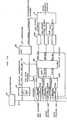
- reference numeral 30 indicates a microcomputer; 31 designates its bus; 32R, 32G and 32B identify a red picture RAM, a green picture RAM and a blue picture RAM, respectively; 33 denotes a priority circuit; 34 represents a priority select circuit; 35 shows a CRT controller; 36R, 36G and 36B refer to parallel-serial converters; 37 signifies a color graphic display; 38 indicates a timing generator; and 39 designates a data update control circuit.
- the red, green and blue picture RAMs 32R, 32G and 32B are writable/readable memories for storing red-colored, green-colored and blue-colored graphic form informations to be displayed on the screen of the color graphic display 37, respectively. Data is written into these memories from the microcomputer 30 and, further, through utilization of the output of the priority circuit 33. Moreover, the picture RAMs can each be accessed from the microcomputer 1 to read out its content at a'desired address and, by the address output of the CRT controller 35, they are accessed in synchronism with one another to scan their contents with a fixed period. The scanned outputs are provided to the priority circuit 33.
- the priority circuit 33 processes the outputs of the thus synchronously accessed RAMs 32R, 32G and 32B in the order of their specified priorities, and provides the output of the RAM with the highest priority to the corresponding parallel-serial converters 36R, 36G and 36B.
- the priority levels of the RAMs 32R, 32G and 32B are specified by the outputs Rl, R0, Gl, G0, B1 and BO of the priority select circuit 34 which is provided with six-bit latches into which data can be written from the microcomputer 30.
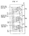
- Fig. 4 is a block diagram of a specific example of the priority circuit 33, illustrating only a processing circuit of one bit of an eight-bit parallel output of each of the picture RAMs 32R, 32G and 32B.
- the one bit output of each picture RAM is input via four lines into all of multiplexers 40R, 40G and 40B, and any one of the four inputs is selected by all of the outputs R1 and R0, Gl and G0, or B1 and BO of the priority select circuit 34.
- Gate circuits 41R to 43R, 41G to 43G and 41B to 43B are each a gate circuit with an inhibit input.
- Fig. 5 shows an example of the relation between the output of the priority select circuit 34 and the selecting operation of the priority circuit 33.
- the priority level A is the highest one and priority C the lowest one.
- the outputs (Rl, R0, G1, G0, Bl, BO) of the priority select circuit 34.are (000000) the outputs of the three RAMs 32R, 32G and 32B are all applied to the parallel-serial converters 36R, 36G and 36B, respectively, since there is no difference in priority among them.
- the red, green and blue picture RAMs 32R, 32G and 32B have stored therein at the same address the information to be displayed, then the corresponding portion of the picture displayed is colored in white.
- the outputs (Rl, R0, G1, G0, B1, BO) are (000111)
- the outputs of the green and blue picture RAMs 32G and 32B are masked by the output of the red picture RAM 32R
- the output of the blue picture RAM 32B is masked by the output of the green picture RAM 32G.
- a total of four bits is sufficient for specifying the priority levels, but the present example employs six bits for the purpose of simplifying-the arrangemnet of the priority circuit 33.
- the parallel-serial converters 36R, 36G and 36B convert eight-bit parallel outputs RDO to RD7, GDO to GD7 and BDO to BD7 of the picture RAMs 32R, 32G and 32B into serial data, which are provided as red, green and blue video signals to the color graphic display 37.
- the color display 37 determines phase differences among chrominance signals according to a combination of the red, green and blue video signals, obtaining a total of eight colors. Horizontal and vertical synchronizing signals of the color display 37 are generated by the CRT controller 35.
- The.outputs of the priority circuit 33 are fed back to the inputs of the red, green and blue picture RAMs 32R, 32 G and 32B, and their contents selected by the output of the data update control circuit 39 can be rewritten by the out-, puts of the priority circuit 33.
- the data update control circuit 39 comprises flip-flops FR, FG and FB for red, green and blue colors, respectively, which can be set and reset by the microcomputer 30, and AND circuits AR, AG and AB for ANDing:the outputs of the flip-flops FR, FG and GB and a write signal from the timing generator 38.
- Outputs WR, WG and WB of the AND circuits AR, AG and AB are input as write signals into the red, green and blue picture RAMs 32R, 32G and 32B.
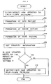
- Fig. 6 is a flowchart showing an example of the software configuration which implements the color display function of a color display unit of the present invention
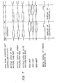
- Fig. 7 is timing chart showing, by way of example, signal waveforms occurring at respective parts of the unit depicted in Fig. 3. A description will be given, with reference to Figs. 6 and 7, of the operation of the unit shown in Figs..3A and B
- the microcomputer 30 resets all the flip-flops FR, FG and FB of the data update control circuit 39 (step P1), and then it writes via the bus 31 into the red, green and blue picture RAMs 32R, 32G and 32B informations of red-colored, green-colored and blue-colored graphic forms to be displayed (steps P2 to P4).
- overlapping of the graphic forms need not be taken into consideration.
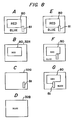
- Fig. 8A in the case of displaying the cutting of a workpiece 80 with a cutter 81, when the workpiece 80 is displayed in red, the cutter 81 in green and the background in blue, such a graphic form of the workpiece 80 as shown in Fig.
- the microcomputer 30 sets in the priority select circuit 34, as its outputs (Rl, R0, Gl, G0, Bl, BO), such information (010011) that gives priorities to the pictures in the order green-red-blue (step P5).
- the priority circuit 33 processes, in accordance with the priorities, the outputs of the red, green and blue picture RAMs 32R, 32G and 32B which are read out in synchronism with one another.
- the graphic forms and the colors of the contents shown in Fig. 8A are displayed on the screen of the color graphic display 37.
- the microcomputer 30 sets that one of the flip-flops of the data update control circuit 39 which corresponds to the RAM that must be updated (steps P6 and P7).
- the flip-flop FR is set and the other flip-flops FG and FB are reset.
- the graphic form of the cutter 81 is moved in the cutting direction while sequentially rewriting the content of the green picture RAM 32G by the microcomputer 30 in a known manner, the picture being displayed undergoes such changes as shown in Figs. 8E, F and G. That is, as shown in the timing chart of Fig. 7, by the write signal which is yielded in synchronism with the outputs RDO to RD7, GDO to GD7 and BDO to BD7 of the priority circuit 33, the content of the red picture RAM 32R alone is rewritten with the outputs R D O to RD7 of the priority circuit 33 corresponding to the red color, so that the portion of the workpiece that has been cut is not displayed but instead the blue-colored background is displayed.
- the three picture RAMs 32R, 32G and 32B are made to correspond to red, green and blue in advance and the priority levels are given to these colors, the correspondence between the colors and the picture RAMs is freely settable and two or more than three RAMs can also be employed. Further, the present invention is applicable not only to the graphic display but also to the character display.
- priority levels are set for a plurality of picture RAMs and that one of the synchronously read out RAM outputs that has a higher priority is taken out by a priority circuit for input into a display, so that even if overlapping graphic forms are to be displayed, the overlap need not be taken into account and it is sufficient only to set the priority levels. This allows ease in the formation of a graph and permits a reduction of the time required therefor.
- a color display unit in which a plurality of picture RAMs (32R,32G,32B) are synchronously accessed by a CRT controller (35), and the priority levels of the outputs from the picture RAMs (32R, 32G,32B) are specified by priority specifying means (34).
- a priority circuit (33) inputs thereinto the outputs of the picture RAMs (32R,32G,32B) and selects the inputs in accordance with the specified priority levels for output to a color display (37).
- the colour display (37) displays, on its CRT screen, graphic forms in colors determined by a combination of the picture RAMs (32R,32G,32B).
- a feedback circuit feeds the output of the priority circuit back to the picture RAMs (32R,32G,32B), and data update control means (39) which specifies which one of the picture RAMs (32R, 32G,32B) is to be rewritten with the output of the feedback circuit are provided.
- data update control means 319 which specifies which one of the picture RAMs (32R, 32G,32B) is to be rewritten with the output of the feedback circuit are provided.
- the stored content of a desired one of the picture RAMs (32R,32G,32B) is thus rewritten with the output of the priority circuit (33).
Abstract
Description
- The present invention relates to a color display unit and, more particularly, to improvements in or relating to a system for specifying a color of each portion of a picture to be displayed in a color display unit.
- With conventional color display units, in the case of putting in colors to respective portions of a picture to be displayed, graphic forms corresponding to the colors are written by software into picture RAMs corresponding to the colors, taking into account the overlap of the graphic forms, and the outputs of the picture RAMs are combined to obtain video signals. For example, in the case where
areas graphic form 5 of thearea 1 to be colored in red, agraphic form 7 of thearea 2 to be colored in green and agraphic form 9 of thearea 3 to be colored in blue are written by software processing into red, green andblue picture RAMs - For obtaining such graphic forms as shown in Figs. 1B to D by finding their intersecting points through software processing, however, a lot of processing is needed, resulting in too much work being imposed on a microprocessor. Especially, when the graphic forms change their positions with time relative to one another, arithmetic processing must be executed for obtaining their intersecting points for each change, so that much time is consumed for the arithmetic processing, making it difficult, in practice, to provide such a colored graphic display.
- According to the invention there is provided a color display unit comprising:
- a plurality of picture RAMs associated with different respective colors;
- write means for writing graphic form informations into the plurality of picture RAMs;
- priority specifying means for specifying priority levels of the outputs of the plurality of picture RAMs;
- a CRT controller for accessing the plurality of picture RAMs in synchronism with one another;
- a priority circuit for outputting, in accordance with the priority levels specified by the priority specifying means, the outputs of the plurality of picture RAMs accessed by the CRT controller; and
- a color display coupled to the output of the priority circuit, for displaying graphic forms in colors determined by a combination of the plurality of picture RAMs.
- An embodiment of the present invention may provide a color display unit which allows ease in providing a colored graphic-display.
- An embodiment of the present invention may provide a color display unit which is capable of putting in colors to a plurality:of graphic forms, as desired, even if they are overlapping.
- An embodiment of the present invention may provide a color display unit which is capable of putting in colors to a plurality of graphic forms by hardware processing, if desired, even if they are overlapping and moving relative to one another.
- In an embodiment of the present invention, graphic forms are produced by software without taking their overlap into account and stored in picture RAMs corresponding to respective colors, and priorities are given to the picture RAMs so that when their outputs are combined, the overlapping graphic forms may be displayed in desired colors. For instance, in the case of displaying such a graphic form of the indicated colors as shown in Fig.lA , circular graphic forms are stored in red, green and
blue picture RAMs - Further, a display unit of the present invention may be provided with a feedback circuit for feeding the output of the priority circuit back to the picture RAMs and data update control means for specifying which one of the picture RAMs is to be rewritten with the output of the feedback circuit. The content of a display is thus modified by hardware processing.
-
- Figs. 1A to D show a series of diagrams explanatory of the operation of a conventional color display unit;
- Figs. 2A to C show a series of diagrams explanatory of the principle of the present invention;
- Figs. 3A and B provide a block diagram illustrating an example of hardware configuration of a color display unit of the present invention;
- Fig. 4 is a block diagram illustrating a specific example of a priority circuit used in the present invention;
- Fig. 5 is a table showing, by way of example, the relationship between the output of a priority select circuit and the selecting operation of the priority circuit;
- Fig. 6 is a flowchart showing an example of the software configuration for implementing the color display function of a color display unit of the present invention;
- Fig: 7 is a timing chart showing, by way of example, signal waveforms occurring at respective parts of the unit shown in Fig. 3; and
- - Fig. 8 shows a series of diagrams explanatory of the operation of 'a. color display unit of the present invention.
- In Figs. 3A and B,
reference numeral 30 indicates a microcomputer; 31 designates its bus; 32R, 32G and 32B identify a red picture RAM, a green picture RAM and a blue picture RAM, respectively; 33 denotes a priority circuit; 34 represents a priority select circuit; 35 shows a CRT controller; 36R, 36G and 36B refer to parallel-serial converters; 37 signifies a color graphic display; 38 indicates a timing generator; and 39 designates a data update control circuit. - The red, green and
blue picture RAMs graphic display 37, respectively. Data is written into these memories from themicrocomputer 30 and, further, through utilization of the output of thepriority circuit 33. Moreover, the picture RAMs can each be accessed from themicrocomputer 1 to read out its content at a'desired address and, by the address output of theCRT controller 35, they are accessed in synchronism with one another to scan their contents with a fixed period. The scanned outputs are provided to thepriority circuit 33. - The
priority circuit 33 processes the outputs of the thus synchronously accessedRAMs serial converters RAMs select circuit 34 which is provided with six-bit latches into which data can be written from themicrocomputer 30. - Fig. 4 is a block diagram of a specific example of the
priority circuit 33, illustrating only a processing circuit of one bit of an eight-bit parallel output of each of thepicture RAMs multiplexers select circuit 34. Gate circuits 41R to 43R, 41G to 43G and 41B to 43B are each a gate circuit with an inhibit input. Fig. 5 shows an example of the relation between the output of the priorityselect circuit 34 and the selecting operation of thepriority circuit 33. It is predetermined that the priority level A is the highest one and priority C the lowest one. For instance, when the outputs (Rl, R0, G1, G0, Bl, BO) of the priority select circuit 34.are (000000), the outputs of the threeRAMs serial converters blue picture RAMs blue picture RAMs red picture RAM 32R, and the output of theblue picture RAM 32B is masked by the output of thegreen picture RAM 32G. Incidentally, a total of four bits is sufficient for specifying the priority levels, but the present example employs six bits for the purpose of simplifying-the arrangemnet of thepriority circuit 33. - In Figs. 3A and B, the parallel-
serial converters picture RAMs graphic display 37. Thecolor display 37, as well-known in the art, determines phase differences among chrominance signals according to a combination of the red, green and blue video signals, obtaining a total of eight colors. Horizontal and vertical synchronizing signals of thecolor display 37 are generated by theCRT controller 35. - The.outputs of the
priority circuit 33 are fed back to the inputs of the red, green andblue picture RAMs update control circuit 39 can be rewritten by the out-, puts of thepriority circuit 33. The dataupdate control circuit 39 comprises flip-flops FR, FG and FB for red, green and blue colors, respectively, which can be set and reset by themicrocomputer 30, and AND circuits AR, AG and AB for ANDing:the outputs of the flip-flops FR, FG and GB and a write signal from thetiming generator 38. Outputs WR, WG and WB of the AND circuits AR, AG and AB are input as write signals into the red, green andblue picture RAMs - Fig. 6 is a flowchart showing an example of the software configuration which implements the color display function of a color display unit of the present invention, Fig. 7 is timing chart showing, by way of example, signal waveforms occurring at respective parts of the unit depicted in Fig. 3. A description will be given, with reference to Figs. 6 and 7, of the operation of the unit shown in Figs..3A and B
- At first, the
microcomputer 30 resets all the flip-flops FR, FG and FB of the data update control circuit 39 (step P1), and then it writes via thebus 31 into the red, green andblue picture RAMs workpiece 80 with acutter 81, when theworkpiece 80 is displayed in red, thecutter 81 in green and the background in blue, such a graphic form of theworkpiece 80 as shown in Fig. 8B is written into thered picture RAM 32R, such a graphic form of thecutter 81 as shown in Fig. 8C is written into thegreen picture RAM 32G and a graphic form the entire area of which is blue as shown in Fig. 8D is written into theblue picture RAM 32B. - Next, the
microcomputer 30 sets in the priorityselect circuit 34, as its outputs (Rl, R0, Gl, G0, Bl, BO), such information (010011) that gives priorities to the pictures in the order green-red-blue (step P5). Thus thepriority circuit 33 processes, in accordance with the priorities, the outputs of the red, green andblue picture RAMs graphic display 37. - When the necessity of updating the content of the RAM arises from the priority setting, the
microcomputer 30 sets that one of the flip-flops of the dataupdate control circuit 39 which corresponds to the RAM that must be updated (steps P6 and P7). In this example, since theworkpiece 80 is cut by thecutter 81, only thered picture RAM 32R has to be updated and, cosequently, the flip-flop FR is set and the other flip-flops FG and FB are reset. - As the graphic form of the
cutter 81 is moved in the cutting direction while sequentially rewriting the content of thegreen picture RAM 32G by themicrocomputer 30 in a known manner, the picture being displayed undergoes such changes as shown in Figs. 8E, F and G. That is, as shown in the timing chart of Fig. 7, by the write signal which is yielded in synchronism with the outputs RDO to RD7, GDO to GD7 and BDO to BD7 of thepriority circuit 33, the content of thered picture RAM 32R alone is rewritten with the outputs RDO to RD7 of thepriority circuit 33 corresponding to the red color, so that the portion of the workpiece that has been cut is not displayed but instead the blue-colored background is displayed. - While in the above example the three
picture RAMs - As has been described in the foregoing, priority levels are set for a plurality of picture RAMs and that one of the synchronously read out RAM outputs that has a higher priority is taken out by a priority circuit for input into a display, so that even if overlapping graphic forms are to be displayed, the overlap need not be taken into account and it is sufficient only to set the priority levels. This allows ease in the formation of a graph and permits a reduction of the time required therefor.
- Moreover, since the contents of the picture RAMs can be modified with the output of the priority circuit, a graphic display can easily be provided which has been substantially impossible because conventional software processing therefor has taken too much time.
- It will be apparent that many modifications and variations may be effected without departing from the scope of the novel concepts of the present invention.
- There has been disclosed a color display unit in which a plurality of picture RAMs (32R,32G,32B) are synchronously accessed by a CRT controller (35), and the priority levels of the outputs from the picture RAMs (32R, 32G,32B) are specified by priority specifying means (34). A priority circuit (33) inputs thereinto the outputs of the picture RAMs (32R,32G,32B) and selects the inputs in accordance with the specified priority levels for output to a color display (37). The colour display (37) displays, on its CRT screen, graphic forms in colors determined by a combination of the picture RAMs (32R,32G,32B). A feedback circuit feeds the output of the priority circuit back to the picture RAMs (32R,32G,32B), and data update control means (39) which specifies which one of the picture RAMs (32R, 32G,32B) is to be rewritten with the output of the feedback circuit are provided. By hardware processing, the stored content of a desired one of the picture RAMs (32R,32G,32B) is thus rewritten with the output of the priority circuit (33).
Claims (2)
Applications Claiming Priority (2)
| Application Number | Priority Date | Filing Date | Title |
|---|---|---|---|
| JP172459/82 | 1982-09-29 | ||
| JP57172459A JPS5960487A (en) | 1982-09-29 | 1982-09-29 | Color display |
Publications (3)
| Publication Number | Publication Date |
|---|---|
| EP0106601A2 true EP0106601A2 (en) | 1984-04-25 |
| EP0106601A3 EP0106601A3 (en) | 1986-02-26 |
| EP0106601B1 EP0106601B1 (en) | 1989-09-20 |
Family
ID=15942382
Family Applications (1)
| Application Number | Title | Priority Date | Filing Date |
|---|---|---|---|
| EP83305878A Expired EP0106601B1 (en) | 1982-09-29 | 1983-09-29 | Color display unit |
Country Status (4)
| Country | Link |
|---|---|
| US (1) | US4628305A (en) |
| EP (1) | EP0106601B1 (en) |
| JP (1) | JPS5960487A (en) |
| DE (1) | DE3380605D1 (en) |
Cited By (2)
| Publication number | Priority date | Publication date | Assignee | Title |
|---|---|---|---|---|
| EP0176801A2 (en) * | 1984-09-05 | 1986-04-09 | Hitachi, Ltd. | A peripheral apparatus for image memories |
| EP0192958A2 (en) * | 1985-01-31 | 1986-09-03 | Siemens Aktiengesellschaft | Display control device |
Families Citing this family (15)
| Publication number | Priority date | Publication date | Assignee | Title |
|---|---|---|---|---|
| JPS61109093A (en) * | 1984-11-02 | 1986-05-27 | 日本電信電話株式会社 | Image display unit |
| JPS61255473A (en) * | 1985-05-08 | 1986-11-13 | Panafacom Ltd | Video information transferring and processing system |
| GB8614874D0 (en) * | 1986-06-18 | 1986-07-23 | Rca Corp | Display processor |
| US4876533A (en) * | 1986-10-06 | 1989-10-24 | Schlumberger Technology Corporation | Method and apparatus for removing an image from a window of a display |
| GB8730363D0 (en) * | 1987-12-31 | 1988-08-24 | British Aerospace | Digital signal processing device |
| US5003496A (en) * | 1988-08-26 | 1991-03-26 | Eastman Kodak Company | Page memory control in a raster image processor |
| US4999780A (en) * | 1989-03-03 | 1991-03-12 | The Boeing Company | Automatic reconfiguration of electronic landing display |
| US5083257A (en) * | 1989-04-27 | 1992-01-21 | Motorola, Inc. | Bit plane partitioning for graphic displays |
| JPH02293792A (en) * | 1989-05-08 | 1990-12-04 | Fujitsu Ten Ltd | Image display device |
| US5258750A (en) * | 1989-09-21 | 1993-11-02 | New Media Graphics Corporation | Color synchronizer and windowing system for use in a video/graphics system |
| US5146554A (en) * | 1989-09-29 | 1992-09-08 | Eastman Kodak Company | Page memory control in a raster image processor employed for digital halftoning |
| US5221921A (en) * | 1989-11-02 | 1993-06-22 | Eastman Kodak Company | High speed character generator |
| WO1992013314A1 (en) * | 1991-01-23 | 1992-08-06 | Seiko Epson Corporation | Image controller |
| US5381158A (en) * | 1991-07-12 | 1995-01-10 | Kabushiki Kaisha Toshiba | Information retrieval apparatus |
| US5808691A (en) * | 1995-12-12 | 1998-09-15 | Cirrus Logic, Inc. | Digital carrier synthesis synchronized to a reference signal that is asynchronous with respect to a digital sampling clock |
Citations (3)
| Publication number | Priority date | Publication date | Assignee | Title |
|---|---|---|---|---|
| US4156237A (en) * | 1976-08-25 | 1979-05-22 | Hitachi, Ltd. | Colored display system for displaying colored planar figures |
| EP0024862A2 (en) * | 1979-09-04 | 1981-03-11 | Harold Charles Taylor | Video apparatus for visualing effects of selected juxtaposed colours |
| DE3035636A1 (en) * | 1980-09-20 | 1982-05-06 | Brown, Boveri & Cie Ag, 6800 Mannheim | Information mixing on VDU - having separate memory containing analogue and digital data to be combined on screen |
Family Cites Families (9)
| Publication number | Priority date | Publication date | Assignee | Title |
|---|---|---|---|---|
| JPS559742B2 (en) * | 1974-06-20 | 1980-03-12 | ||
| GB1593309A (en) * | 1977-12-09 | 1981-07-15 | Ibm | Character graphics colour display system |
| JPS55166687A (en) * | 1979-06-13 | 1980-12-25 | Hitachi Ltd | Graphic display unit |
| JPS5916275B2 (en) * | 1980-06-02 | 1984-04-14 | 株式会社柏木研究所 | graphic display device |
| JPS5781294A (en) * | 1980-11-10 | 1982-05-21 | Hitachi Ltd | Prior color indication system |
| US4439760A (en) * | 1981-05-19 | 1984-03-27 | Bell Telephone Laboratories, Incorporated | Method and apparatus for compiling three-dimensional digital image information |
| US4484187A (en) * | 1982-06-25 | 1984-11-20 | At&T Bell Laboratories | Video overlay system having interactive color addressing |
| US4595917A (en) * | 1983-06-13 | 1986-06-17 | Vectrix Corporation | Data processing technique for computer color graphic system |
| US4580135A (en) * | 1983-08-12 | 1986-04-01 | International Business Machines Corporation | Raster scan display system |
-
1982
- 1982-09-29 JP JP57172459A patent/JPS5960487A/en active Granted
-
1983
- 1983-09-29 US US06/536,877 patent/US4628305A/en not_active Expired - Fee Related
- 1983-09-29 EP EP83305878A patent/EP0106601B1/en not_active Expired
- 1983-09-29 DE DE8383305878T patent/DE3380605D1/en not_active Expired
Patent Citations (3)
| Publication number | Priority date | Publication date | Assignee | Title |
|---|---|---|---|---|
| US4156237A (en) * | 1976-08-25 | 1979-05-22 | Hitachi, Ltd. | Colored display system for displaying colored planar figures |
| EP0024862A2 (en) * | 1979-09-04 | 1981-03-11 | Harold Charles Taylor | Video apparatus for visualing effects of selected juxtaposed colours |
| DE3035636A1 (en) * | 1980-09-20 | 1982-05-06 | Brown, Boveri & Cie Ag, 6800 Mannheim | Information mixing on VDU - having separate memory containing analogue and digital data to be combined on screen |
Cited By (4)
| Publication number | Priority date | Publication date | Assignee | Title |
|---|---|---|---|---|
| EP0176801A2 (en) * | 1984-09-05 | 1986-04-09 | Hitachi, Ltd. | A peripheral apparatus for image memories |
| EP0176801A3 (en) * | 1984-09-05 | 1988-11-09 | Hitachi, Ltd. | A peripheral apparatus for image memories |
| EP0192958A2 (en) * | 1985-01-31 | 1986-09-03 | Siemens Aktiengesellschaft | Display control device |
| EP0192958A3 (en) * | 1985-01-31 | 1990-05-23 | Siemens Aktiengesellschaft | Display control device |
Also Published As
| Publication number | Publication date |
|---|---|
| EP0106601B1 (en) | 1989-09-20 |
| US4628305A (en) | 1986-12-09 |
| JPH0160155B2 (en) | 1989-12-21 |
| DE3380605D1 (en) | 1989-10-26 |
| JPS5960487A (en) | 1984-04-06 |
| EP0106601A3 (en) | 1986-02-26 |
Similar Documents
| Publication | Publication Date | Title |
|---|---|---|
| EP0106601B1 (en) | Color display unit | |
| JP2583003B2 (en) | Image display method, frame buffer, and graphics display system in graphics display system | |
| US4703317A (en) | Blinking of a specific graph in a graphic display | |
| JPH04226495A (en) | Apparatus, system and method for controlling overlay plane in graphic display system | |
| JP2579362B2 (en) | Screen display device | |
| US4763118A (en) | Graphic display system for personal computer | |
| JPS59146309A (en) | Color graphic display device for nc | |
| US4959643A (en) | Display unit having an improved editing input capability | |
| JPH03206492A (en) | Window priority encoder | |
| JPS6226472B2 (en) | ||
| JPH0421207B2 (en) | ||
| JPS62198908A (en) | Drawing method for numerical controller | |
| EP0763934A2 (en) | System for on-screen-display | |
| JPS6193494A (en) | Display color controller | |
| JPS60144793A (en) | Color display unit | |
| JPH022150B2 (en) | ||
| JPS6095492A (en) | Display modification controller | |
| JPS6079394A (en) | Color graphic display unit | |
| JPS63213890A (en) | Information processing system | |
| JPH0128388B2 (en) | ||
| JPS6267589A (en) | Color display unit | |
| JPS60175088A (en) | Graphic display | |
| JPS6324290A (en) | Screen synthesization circuit | |
| JPS5972513A (en) | Nc color display device | |
| JPH0642131B2 (en) | Display color control circuit for display device |
Legal Events
| Date | Code | Title | Description |
|---|---|---|---|
| PUAI | Public reference made under article 153(3) epc to a published international application that has entered the european phase |
Free format text: ORIGINAL CODE: 0009012 |
|
| AK | Designated contracting states |
Designated state(s): DE FR GB |
|
| PUAL | Search report despatched |
Free format text: ORIGINAL CODE: 0009013 |
|
| AK | Designated contracting states |
Designated state(s): DE FR GB |
|
| 17P | Request for examination filed |
Effective date: 19860725 |
|
| 17Q | First examination report despatched |
Effective date: 19880825 |
|
| GRAA | (expected) grant |
Free format text: ORIGINAL CODE: 0009210 |
|
| AK | Designated contracting states |
Kind code of ref document: B1 Designated state(s): DE FR GB |
|
| REF | Corresponds to: |
Ref document number: 3380605 Country of ref document: DE Date of ref document: 19891026 |
|
| ET | Fr: translation filed | ||
| PLBE | No opposition filed within time limit |
Free format text: ORIGINAL CODE: 0009261 |
|
| STAA | Information on the status of an ep patent application or granted ep patent |
Free format text: STATUS: NO OPPOSITION FILED WITHIN TIME LIMIT |
|
| 26N | No opposition filed | ||
| PGFP | Annual fee paid to national office [announced via postgrant information from national office to epo] |
Ref country code: FR Payment date: 19930909 Year of fee payment: 11 |
|
| PGFP | Annual fee paid to national office [announced via postgrant information from national office to epo] |
Ref country code: GB Payment date: 19930921 Year of fee payment: 11 |
|
| PGFP | Annual fee paid to national office [announced via postgrant information from national office to epo] |
Ref country code: DE Payment date: 19930922 Year of fee payment: 11 |
|
| PG25 | Lapsed in a contracting state [announced via postgrant information from national office to epo] |
Ref country code: GB Effective date: 19940929 |
|
| GBPC | Gb: european patent ceased through non-payment of renewal fee |
Effective date: 19940929 |
|
| PG25 | Lapsed in a contracting state [announced via postgrant information from national office to epo] |
Ref country code: FR Effective date: 19950531 |
|
| PG25 | Lapsed in a contracting state [announced via postgrant information from national office to epo] |
Ref country code: DE Effective date: 19950601 |
|
| REG | Reference to a national code |
Ref country code: FR Ref legal event code: ST |