EP0104536A2 - Microstrip reflect array for satellite communication and radar cross-section enhancement or reduction - Google Patents
Microstrip reflect array for satellite communication and radar cross-section enhancement or reduction Download PDFInfo
- Publication number
- EP0104536A2 EP0104536A2 EP83109018A EP83109018A EP0104536A2 EP 0104536 A2 EP0104536 A2 EP 0104536A2 EP 83109018 A EP83109018 A EP 83109018A EP 83109018 A EP83109018 A EP 83109018A EP 0104536 A2 EP0104536 A2 EP 0104536A2
- Authority
- EP
- European Patent Office
- Prior art keywords
- reflectarray
- microstrip
- microstrip antenna
- transmission line
- array
- Prior art date
- Legal status (The legal status is an assumption and is not a legal conclusion. Google has not performed a legal analysis and makes no representation as to the accuracy of the status listed.)
- Withdrawn
Links
Images


Classifications
-
- H—ELECTRICITY
- H01—ELECTRIC ELEMENTS
- H01Q—ANTENNAS, i.e. RADIO AERIALS
- H01Q21/00—Antenna arrays or systems
- H01Q21/06—Arrays of individually energised antenna units similarly polarised and spaced apart
- H01Q21/061—Two dimensional planar arrays
- H01Q21/065—Patch antenna array
-
- H—ELECTRICITY
- H01—ELECTRIC ELEMENTS
- H01Q—ANTENNAS, i.e. RADIO AERIALS
- H01Q3/00—Arrangements for changing or varying the orientation or the shape of the directional pattern of the waves radiated from an antenna or antenna system
- H01Q3/44—Arrangements for changing or varying the orientation or the shape of the directional pattern of the waves radiated from an antenna or antenna system varying the electric or magnetic characteristics of reflecting, refracting, or diffracting devices associated with the radiating element
- H01Q3/46—Active lenses or reflecting arrays
Definitions
- This invention is directed generally to antenna structures for receiving/transmitting r.f. electromagnetic fields. More particularly, it is directed to a "reflectarray" organization of microstrip antenna radiator elements of the type that are typically disposed less than one-tenth wavelength above a ground or reference conductor so as to define a resonant cavity between each such radiator element and the underlying ground surface while at the same time also defining at least one radiation slot between an edge of the radiator element and the underlying ground plane surface for coupling r.f. energy to/from the element at an intended antenna operating frequency.
- microstrip antenna radiator elements or "patches” are formed by selective photo-chemical etching of a metallically cladded . surface on a dielectric layer so as to produce essentially two-dimensional conductive areas where at least one of those dimensions is resonant (within the dielectric layer) at the intended antenna operating frequency.
- Microstrip antenna radiator elements or "patches" per se and/or various arrays of such elements are by now well known in the art.
- some typical prior art microstrip antenna structures are disclosed in the following prior issued U.S. patents:
- reflectarray structures utilizing other types of elementary antenna elements are also well known in the art. For example, reference may be had to:
- microstrip reflectarrays may offer substantial commercial advantages when applied to satellite communication problems.
- the most common antenna system for receiving r.f. fields from an earth satellite station typically comprised a large parabolic-shaped dish reflector having a primary r.f. receiver (e.g., a waveguide horn) at the focal point of the shaped reflector dish.
- a primary r.f. receiver e.g., a waveguide horn
- Such a dish is not only relatively expensive to form, it is relatively heavy and bulky and difficult if not impossible to visually camouflage for aesthetic or other reasons. It is also quite vulnerable to several adverse environmental parameters (e.g., wind, temperature, etc.).
- microstrip antenna array structure as a "reflectarray" such that the antenna array acts as a passive-shaped reflector directing incident r.f. energy toward a feed system focal area or spot where a waveguide horn or the like is located.
- the antenna array itself thus remains effective as a very efficient collector of incident microwave r.f. electromagnetic energy. (I.e., losses otherwise involved in the conventional feedline structure associated with the microstrip array are avoided.)
- many of the problems associated with prior art parabolic-shaped metallic dish reflectors e.g., mechanical stability, wind loading, etc.
- the microstrip reflectarray which can be simply affixed (e.g., with adhesives, nails, screws, or any other conventional technique of affixation) to a flat (or other shape) wall on the south side of a building for satellite television reception or the like (assuming that the earth satellite station of interest is located in a geo-stationary orbit in the southern sky -- as is currently the case for many applications).
- microstrip reflectarray structure will retain all of the usual advantages associated with microstrip antenna structures (e.g., they may be made so as to be conformable to other than flat surfaces, easily retrofitted so as to replace other types of antenna structures, simply fabricated using photo-chemical processes with relatively inexpensive materials so as to produce a monolithic structure capable of withstanding relatively high static and/or dynamic mechanical loads, temperatures, etc.).
- the monolithic low profile microstrip phased reflectarray of this invention utilizes microstrip radiating elements having half-wavelength resonant dimensions.
- Each microstrip radiator element is individually “phased” by connection to a specified phase length of microstrip line (1) to effectively cause the incident field to be steered so as to direct it to a desired position (e.g., a waveguide feedhorn or the like), or (2) to enhance the retro-reflected field (e.g., so as to enhance the radar cross-section of the object to which the reflectarray is attached or conformed) or to reduce the retro-reflected field (e.g., so as to reduce the radar cross-section of the object to which the reflectarray is attached or conformed).
- the phasing microstrip transmission lines are individually terminated (e.g., an open circuit, a short circuit, a particular type of inductive or capacitive impedance, a resistive lossy impedance, a switchable diode connected in series with such a termination, etc.) depending upon the type of application involved.
- terminated e.g., an open circuit, a short circuit, a particular type of inductive or capacitive impedance, a resistive lossy impedance, a switchable diode connected in series with such a termination, etc.
- this same microstrip reflectarray structure may be easily configured so as to either enhance or reduce the radar cross-section of the object to which it is attached or conformed.
- the reflectarray can be designed and placed on the object (e.g., conformed to its natural shape) so as to enhance the amount of incident radar energy retro-reflected toward the originating radar set.
- the reverse of this phenomenon is also achievable where a reduction in the retro-reflected radar energy may be desired.
- the microstrip reflectarray aperture would be phased so as to re-direct or scatter the incident radar energy away from the retro-reflect direction so as to effectively reduce the radar cross-section.
- This latter application may also employ lossy resistive loading of the microstrip feedlines or possibly the use of a resistive dielectric substrate throughout the whole of the microstrip reflectarray structure (i.e., between the radiator patches and the underlying ground plane) so as to help absorb the incident r.f. power.
- the microstrip reflectarray structure of this invention tends to minimize feedline losses thus enhancing the effective utility of microstrip antenna arrays for satellite communication purposes while at the same time reducing costs, providing a less complicated mechanical structure and other advantages as already mentioned. Enhancement or reduction of radar cross-sections can be obtained using this same type of microstrip reflectarray. By properly phasing the array aperture, back scattered radiation energy retro-reflected from an object can be increased. Alternatively, by resistively loading the microstrip lines, incident radar power can be absorbed.
- the incident radar energy can be both re-directed and partially absorbed so as to even better minimize the radar cross-section.
- the microstrip reflectarray uses half wave resonant rectangular microstrip patches located on a dielectric substrate with a conducting ground plane. Each element is attached to a microstrip transmission line or to a feedthrough pin to a transmission line. The transmission lines are used to phase-the array so as to direct any re-transmitted field in a preferred direction.
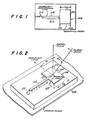
- a typical microstrip antenna element is depicted in FIGURES 1 and 2. It includes a resonantly dimensioned radiating patch 100 (a very thin essentially two-dimensional electrically conductive area) closely spaced above an electrically conducting ground plane or reference surface 102 (typically spaced less than one-tenth of a wavelength at the intended antenna operating frequency above the ground plane).
- the radiating patch 100 has a resonant dimension of one-half wavelength thus defining a one-half wavelength resonant cavity 104 between the radiating patch and the ground plane surface 102.
- opposite transverse edges 104, 106 define radiating slots 108, 110 with the underlying ground plane surface.
- the non-resonant transverse dimension is typically substantially in excess of one-half wavelength but less than a complete wavelength. If the transverse dimension approaches one wavelength or more at the intended antenna operating frequency, then plural feedpoints are preferably utilized (e.g., at least one for every wavelength of transverse dimension) as those in the art will appreciate.
- microstrip antenna elements of various shapes (e.g., rectangular, square, circular, elliptical and various other shapes including quarter- wavelength resonant dimensions where one side of the resonant cavity is effectively r.f. shorted to the underlying ground plane by pins or other means) are well known in the art.
- a relatively thin dielectric layer e.g., Teflon, fiberglass of 1/32 inch thickness
- is copper cladded on both sides e.g., .001 inch thick copper coating
- One copper cladded side of the dielectric sheet is typically left intact as the ground or reference surface 102 while the other is selectively etched (e.g., by conventional photo-chemical etching processes similar to those used for the formation of printed circuit boards and the like) to leave one or more resonantly dimensioned radiating patches 100.
- the feedlines are typically provided as a corporate structured or other series/parallel network such that all patches included in a given antenna array are fed by a common r.f. input/output port.
- a feedthrough pin e.g., the center conductor of a coaxial cable
- the presently preferred exemplary embodiment utilizes integrally formed and connected microstrip transmission lines 112 coupled to impedance matched feedpoints of respectively associated microstrip patches 100.
- the individual feedline 112 is terminated at 114 and typically has a length equal to some fraction K of a complete wavelength.
- Incident r.f. radiation fields 116 are then coupled to the microstrip patch 100 and resonant cavity 104 via the radiating slots 108, 110 and converted to corresponding r.f. electrical currents which propagate along the microstrip transmission line 112 toward termination 114.
- the termination 11 4 will typically include lossy resistive components or materials so as to dissipate the r.f. electrical currents (i.e., as heat).
- the termination 114 will typically be reactive (i.e., so as to produce a desired additional incremental phase shift or the like) or an open circuit or a short circuit condition.
- the currents are reflected by along the transmission 112 and re-radiated from the radiating slots 108, 110 assocciated with the resonantly dimensioned microstrip patch 100 and resonant cavity 104.
- the fractional wavelength length of the microstrip transmission line 112 is effectively doubled since the r.f. electrical currents traverse this transmission line segment twice if they are reflected from the termination 114.
- the resulting phase shift thus encountered before the r.f. energy is re-transmitted is a function both of the transmission length and of the type of termination 114.
- the incident r.f. field 116 is assumed to be a plane wave directed at an angle 9 i with respect to a normal line to the patch 100 (as depicted in FIGURE 2), then some portion of the incident field will naturally be reflected at an equal 9 r in accordance with Snell's law. In addition, some portion of the field will be transmitted into, i.e., coupled to the cavity 104 (typically a dielectric structure as earlier mentioned) via the radiating slots. In addition, where transmission line 112 has been terminated so as to cause substantial reflection of r.f. electrical currents, there will be re-transmitted fields (depicted at 116, 118 in FIGURE 2) emanating from the radiating slots 108, 110.
- the re-transmitted field may be caused to be re-directed at a predetermined angle 9a as indicated in FIGURES 3-5 which depict such a microstrip reflectarray.
- FIGURES 1 and 2 show the physical phenomenon of a single half-wave microstrip reflecting patch.
- the reflecting element is resonated through an incident plane wave field which is somewhat different than the standard microstrip antenna excitation using a coaxial feed section from ground plane side or through edge launching into a microstrip transmission line.
- the incident field partially is coupled into the microstrip resonant element, the remainder is reflected and/or transmitted into the dielectric substrate.
- the field coupled into the microstrip element propagates into the transmission line with certain type of end load. A reflection of the signal will be encountered depending on the load condition.
- a two-way phase shift is expected through the transmission line. The choice of phase shift determines the re-directed radiation characteristic of the reflectarray.
- a matched load at the end of each transmission line will absorb the coupled field.
- a short or an open load will reflect the field with a two-way phase shift.
- the selection of these transmission lines and end loads will depend on the type of application (satellite antennas, radar antennas, radar cross-section enchance or reduction).
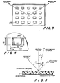
- FIGURES 3-5 A 4X5 element microstrip reflectarray is indicated. It will be noted that the length of the transmission line segments is different for each of the four horizontal rows of elements.
- the showing in FIGURE 3 is arbitrary and solely for the purpose of indicating that any desired two-dimensional phase taper across the two-dimensional aperture of the array may be achieved in accordance with conventional design of phase tapered array apertures.
- the transmission line segments may be meandered so as to fit within the available space as should be apparent to those in the art, especially in view of FIGURE 3.
- the transmission line termination (e.g., open circuit, short circuit, resistive or reactive loads as may be desired for any given application) is schematically depicted by a truncated triangle in FIGURE 4.
- FIGURE 5 The cross-sectional schematic depiction of FIGURE 5 is similar to that of FIGURE 2 except that in the context of the FIGURE 3 reflectarray, there is now shown a vector representing the re-directed r.f. field at an arbitrary angle 8 d from the normal line.
- conventional antenna array design techniques may be utilized for defining the required phase taper of the array aperture to achieve a desired 8 d given a known incident field orientation and thus a known incident phase taper across the aperture.
- a flat reflectarray 200 depicted in FIGURE 2 and in more detail at FIGURE 11 may be associated with a receiver/transmitter microwave horn structure 202 to form part of an earth satellite communication system.
- a receiver/transmitter microwave horn structure 202 may be associated with a receiver/transmitter microwave horn structure 202 to form part of an earth satellite communication system.
- the reflectarray 200 in this exemplary embodiment has been provided with a one-dimensional parabolic phase taper across its two-dimensional aperture. Accordingly, as will be observed by reference to the more detailed FIGURE 11, there is but a single plane of symmetry passing mid-way between the eight vertical columns of individual antenna elements (i.e., symmetry vis-a-vis the relative phasing of individual antenna elements as can be observed by the relative lengths of terminated transmission line connected to each element).
- This particular phase taper has been designed (using conventional microstrip array design techniques) so as to re-direct an incident planewave of electromagnetic r.f. radiation (in the C-band at approximately 3.9 GHz) from a typical geostationary satellite as viewed in the vicinity of Boulder, Colorado.
- the exemplary microstrip reflectarray embodiment depicted in FIGURE 11 has been successfully tested using the following design criteria:
- FIGURES 6 and 11 were only constructed and tested using a one-dimensional parabolic phase taper across one axis or dimension of the array aperture (i.e., from side to side in FIGURE 11), it should be appreciated that even greater efficiency can be expected by providing a two-dimensional parabolic phase taper with a more concentrated focal spot or area (or other desired phase tapers that effectively result in concentrating re-directed energy from the reflectarray to a common receive/transmit feedpoint such the horn 202 in FIGURE 5) could be achieved.
- the microstrip reflectarray of this invention may also be electronically controlled as depicted in FIGURE 7.
- each of the individual microstrip antenna elements has a series of electronically switchable phase shifters connected in its individually associated transmission line structure.
- a conventional three-bit electronic phase shifter is employed such that any desired combination of 180° and/or 90° and/or 45° relative phase shift can be attained by appropriately controlling diode switches in the transmission line structure.
- microstrip reflectarray of this invention need not be limited to linearly polarized individual array elements.
- circularly and/or elliptically polarized microstrip antenna elements may be employed as depicted in FIGURES 8, 9 and 10. Since all of these microstrip antenna elements are per se well known in the art, only a very brief description need be given here.
- the microstrip radiator patches are substantially square-shaped but have feedpoints on adjacent sides that are phased relative to one another by 90°.
- the 90° phase shifter feed network is schematically depicted in FIGURE 8. Also depicted are various length terminated transmission line segments connected, in turn, to the feedpoint of the 90° phase shifter circuit.
- one dimension of the almost square microstrip patches is altered slightly so as to cause the r.f. impedance along orthogonal axes to be approximately complex conjugates of each other or other desired relationships.
- Circular and/or elliptical polarization can then be had by merely feeding each patch near a corner point as indicated in FIGURE 9.
- the feedpoints are connected to individually terminated transmission line segments which have lengths chosen so as to achieve a desired phase taper across the array aperture.
- FIGURE 10 Another exemplary circular or elliptical polarization embodiment of the microstrip reflectarrary is depicted at FIGURE 10 where substantially circular microstrip patches are fed at two different points separated by 90° and fed by signals having 90° relative phase different.
- the 90° relative phase differences can, for example, be provided by 90° hybrid transmission line circuits provided on a second layered hybrid board with pin connectors extending through to the feedpoints of the circular patches, etc., in accordance with conventional practice.
- FIGURE 12 depicts a portion of a cylindrical projectile having spring-loaded cylindrical segments that automatically extend during flight to expose microstrip reflectarrays constructed in accordance with this invention.
- the microstrip reflectarray 300 (a 4x16 element array in this exemplary embodiment) is then provided with a one-dimensional phase taper (i.e., across the long dimension of the array aperture with relative phasing of 0°, 90°, 180°, 270°, 0°, etc.) so as to produce an "end fire" radiation pattern for the re-directed energy.
- a one-dimensional phase taper i.e., across the long dimension of the array aperture with relative phasing of 0°, 90°, 180°, 270°, 0°, etc.
- the end fire radiation pattern of the microstrip reflectarray 300 causes an essentially retro-reflection of the incident radar field.
- Substantial enhancement of the radar cross-section results.
- the exemplary microstrip reflectarray 300 is shown in more detail at FIGURE 13.
- the incident field may also be caused to be steered in a direction other than the retro-reflection direction and/or to be randomly scattered (i.e., by properly controlling an electronically steered microstrip reflectarray).
- the incident field may be absorbed by resistive loads at the transmission line terminations and/or distributed resistive loads throughout the dielectric substrate.
Abstract
Description
- This invention is directed generally to antenna structures for receiving/transmitting r.f. electromagnetic fields. More particularly, it is directed to a "reflectarray" organization of microstrip antenna radiator elements of the type that are typically disposed less than one-tenth wavelength above a ground or reference conductor so as to define a resonant cavity between each such radiator element and the underlying ground surface while at the same time also defining at least one radiation slot between an edge of the radiator element and the underlying ground plane surface for coupling r.f. energy to/from the element at an intended antenna operating frequency. Typically, such microstrip antenna radiator elements or "patches" are formed by selective photo-chemical etching of a metallically cladded . surface on a dielectric layer so as to produce essentially two-dimensional conductive areas where at least one of those dimensions is resonant (within the dielectric layer) at the intended antenna operating frequency.
- Microstrip antenna radiator elements or "patches" per se and/or various arrays of such elements are by now well known in the art. For example, some typical prior art microstrip antenna structures are disclosed in the following prior issued U.S. patents:


- As those in the art will appreciate, the above list is by no means exhaustive.
- As a general concept, reflectarray structures utilizing other types of elementary antenna elements are also well known in the art. For example, reference may be had to:
- 1. M.I. Skolnik, "Introduction to Radar Systems", McGraw-Hill, 1980, pages 308-309;
- 2. M.I. Skolnik, "Radar Handbook", Chapter 11, Array Antennas by Theodore C. Cheston and Joe Frank, McGraw-Hill, 1970, pages 11-54 through 11-60;
- 3. G.T. Ruck, D.E. Barrick, W.D. Stuart and C.K. Krichbaum, "Radar Cross-Section Handbook",
Volumes 1 and 2, Plenum Press, New York, 1970, pages 585-670; and - 4. H. Jasik, "Antenna Engineering Handbook", Chapter 13, by W.C. Jakes and S.D. Robertson, McGraw-Hill, 1961, pages 13-1 through 13-14.
- General theoretical considerations on enhancing and reducing radar cross-sections are also found in "Method of Radar Cross-Section Analysis* by J.W. Crispin and Km. Siegel, Academic Press, 1968.
- In spite of such general knowledge in the prior art of microstrip antenna elements and arrays per se and of reflectarrays using other types of antenna elements, so far as we are aware, before our invention no one has utilized a reflectarray formed of microstrip antenna radiator elements. However, as explained more fully below, we have now discovered many quite advantageous potential uses for such a microstrip species of reflectarray which uses promise to make the microstrip reflectarray a very welcome practical solution to several long-standing technical and/or commercial problems in the relevant art.
- For example, microstrip reflectarrays may offer substantial commercial advantages when applied to satellite communication problems. Heretofore, the most common antenna system for receiving r.f. fields from an earth satellite station typically comprised a large parabolic-shaped dish reflector having a primary r.f. receiver (e.g., a waveguide horn) at the focal point of the shaped reflector dish. Such a dish is not only relatively expensive to form, it is relatively heavy and bulky and difficult if not impossible to visually camouflage for aesthetic or other reasons. It is also quite vulnerable to several adverse environmental parameters (e.g., wind, temperature, etc.).
- Attempts to design microstrip antenna arrays for satellite communication applications using the conventional corporate, series or other intricate feedline structures to feed the individual microstrip radiator elements with respect to a common input/output port often become impractical where large arrays are concerned due to the relatively large losses involved in the lengthy microstrip feedlines at the relatively high frequencies involved. However, we have now discovered that these problems can be overcome by designing the microstrip antenna array structure as a "reflectarray" such that the antenna array acts as a passive-shaped reflector directing incident r.f. energy toward a feed system focal area or spot where a waveguide horn or the like is located.
- The antenna array itself thus remains effective as a very efficient collector of incident microwave r.f. electromagnetic energy. (I.e., losses otherwise involved in the conventional feedline structure associated with the microstrip array are avoided.) In addition, many of the problems associated with prior art parabolic-shaped metallic dish reflectors (e.g., mechanical stability, wind loading, etc.) are simultaneously alleviated by using the microstrip reflectarray which can be simply affixed (e.g., with adhesives, nails, screws, or any other conventional technique of affixation) to a flat (or other shape) wall on the south side of a building for satellite television reception or the like (assuming that the earth satellite station of interest is located in a geo-stationary orbit in the southern sky -- as is currently the case for many applications).
- At the same time, the microstrip reflectarray structure will retain all of the usual advantages associated with microstrip antenna structures (e.g., they may be made so as to be conformable to other than flat surfaces, easily retrofitted so as to replace other types of antenna structures, simply fabricated using photo-chemical processes with relatively inexpensive materials so as to produce a monolithic structure capable of withstanding relatively high static and/or dynamic mechanical loads, temperatures, etc.).
- In the presently preferred exemplary embodiment, the monolithic low profile microstrip phased reflectarray of this invention utilizes microstrip radiating elements having half-wavelength resonant dimensions. Each microstrip radiator element is individually "phased" by connection to a specified phase length of microstrip line (1) to effectively cause the incident field to be steered so as to direct it to a desired position (e.g., a waveguide feedhorn or the like), or (2) to enhance the retro-reflected field (e.g., so as to enhance the radar cross-section of the object to which the reflectarray is attached or conformed) or to reduce the retro-reflected field (e.g., so as to reduce the radar cross-section of the object to which the reflectarray is attached or conformed). The phasing microstrip transmission lines are individually terminated (e.g., an open circuit, a short circuit, a particular type of inductive or capacitive impedance, a resistive lossy impedance, a switchable diode connected in series with such a termination, etc.) depending upon the type of application involved.
- As just mentioned, we have also discovered that this same microstrip reflectarray structure may be easily configured so as to either enhance or reduce the radar cross-section of the object to which it is attached or conformed. For example, if an object inherently has a relatively low radar cross-section and no large protrusion is allowed, the reflectarray can be designed and placed on the object (e.g., conformed to its natural shape) so as to enhance the amount of incident radar energy retro-reflected toward the originating radar set. Of course, the reverse of this phenomenon is also achievable where a reduction in the retro-reflected radar energy may be desired. For this latter application, the microstrip reflectarray aperture would be phased so as to re-direct or scatter the incident radar energy away from the retro-reflect direction so as to effectively reduce the radar cross-section. This latter application may also employ lossy resistive loading of the microstrip feedlines or possibly the use of a resistive dielectric substrate throughout the whole of the microstrip reflectarray structure (i.e., between the radiator patches and the underlying ground plane) so as to help absorb the incident r.f. power.
- Among other advantages, for a satellite antenna array application, the microstrip reflectarray structure of this invention tends to minimize feedline losses thus enhancing the effective utility of microstrip antenna arrays for satellite communication purposes while at the same time reducing costs, providing a less complicated mechanical structure and other advantages as already mentioned. Enhancement or reduction of radar cross-sections can be obtained using this same type of microstrip reflectarray. By properly phasing the array aperture, back scattered radiation energy retro-reflected from an object can be increased. Alternatively, by resistively loading the microstrip lines, incident radar power can be absorbed. By both appropriately tapering the array aperture so as to misdirect any re-transmitted energy away from the retro-reflection direction and/or by resistively loading the array structure, the incident radar energy can be both re-directed and partially absorbed so as to even better minimize the radar cross-section.
- In the exemplary embodiments, the microstrip reflectarray uses half wave resonant rectangular microstrip patches located on a dielectric substrate with a conducting ground plane. Each element is attached to a microstrip transmission line or to a feedthrough pin to a transmission line. The transmission lines are used to phase-the array so as to direct any re-transmitted field in a preferred direction.
- These as well other objects and advantages of this invention will be better understood and appreciated by a careful reading of the following detailed description of the presently preferred exemplary embodiments of this invention in conjunction with the accompanying drawings, of which:
- FIGURES 1 and 2 are a plan and perspective view respectively of a single microstrip radiating patch and its associated terminated transmission line segment of the type that may be replicated and arrayed in a microstrip reflectarray in accordance with this invention;
- FIGURE 3 is a plan view of an arbitrary exemplary microstrip reflectarray constructed in accordance with this invention using the microstrip patch/line elements of FIGURES 1 and 2;
- FIGURE 4 is an enlarged view of one of the array elements and its associated terminated transmission line as specifically configured in the array of FIGURE 3;
- FIGURE 5 is a schematic cross-sectional depiction of the array shown in FIGURE 3 together with vectors representing incident, reflected, re-directed and transmitted r.f. fields;
- FIGURE 6 is a perspective view of an antenna system for receiving/ transmitting r.f. electromagnetic radiation from/to an earth satellite sation which includes a microstrip reflectarray in accordance with this invention and as depicted in FIGURES 1-5 having a parabolic phase taper across at least one dimension of the array aperture so as to re-direct r.f. radiation to/from a microwave horn structure;
- FIGURE 7 is an alternative microstrip reflectarrary in accordance with this invention including electronically controlled phase shifters so as to permit the re-directed r.f. radiation to be switched between different beam positions;
- FIGURES 8, 9 and 10 depict various circularly polarized and/or elliptically polarized microstrip reflectarray embodiments in accordance with this invention;
- FIGURE 11 is a more detailed showing of an exemplary microstrip reflectarray for use in a ground satellite communication system of the type shown in FIGURE 6 where one dimension of the array aperture has been given a parabolic phase taper;
- FIGURE 12 generally depicts a projectile casing having spring-loaded cylinder segments which open in flight to expose microstrip reflectarray antennas designed in accordance with this invention so as to have "end fire" re-direction capabilities thus enhancing the radar cross-section of the projectile as it is viewed by a radar set directed to strike the rear of the moving projectile; and
- FIGURE 13 is an expanded view of one of the microstrip reflectarrays used in FIGURE 12.
- A typical microstrip antenna element is depicted in FIGURES 1 and 2. It includes a resonantly dimensioned radiating patch 100 (a very thin essentially two-dimensional electrically conductive area) closely spaced above an electrically conducting ground plane or reference surface 102 (typically spaced less than one-tenth of a wavelength at the intended antenna operating frequency above the ground plane). In the exemplary embodiment of FIGURES 1 and 2, the radiating
patch 100 has a resonant dimension of one-half wavelength thus defining a one-half wavelengthresonant cavity 104 between the radiating patch and the ground plane surface 102. In this exemplary embodiment, oppositetransverse edges 104, 106 define radiatingslots - Such microstrip antenna elements of various shapes (e.g., rectangular, square, circular, elliptical and various other shapes including quarter- wavelength resonant dimensions where one side of the resonant cavity is effectively r.f. shorted to the underlying ground plane by pins or other means) are well known in the art. Typically, a relatively thin dielectric layer (e.g., Teflon, fiberglass of 1/32 inch thickness) is copper cladded on both sides (e.g., .001 inch thick copper coating) as a starting material. One copper cladded side of the dielectric sheet is typically left intact as the ground or reference surface 102 while the other is selectively etched (e.g., by conventional photo-chemical etching processes similar to those used for the formation of printed circuit boards and the like) to leave one or more resonantly dimensioned radiating
patches 100. In addition, it is currently typical practice to simultaneously and integrally form connected microstrip transmission feedlines for feeding r.f. energy to/from the resonantly dimensioned radiating patches. The feedlines are typically provided as a corporate structured or other series/parallel network such that all patches included in a given antenna array are fed by a common r.f. input/output port. Alternatively, it is also conventional practice to feed the individual microstrip antenna elements by connecting (e.g., soldering or the like) a feedthrough pin (e.g., the center conductor of a coaxial cable) extending through the dielectric substrate and to a feedpoint within the radiating patch that provides a matched impedance feed. - The presently preferred exemplary embodiment utilizes integrally formed and connected
microstrip transmission lines 112 coupled to impedance matched feedpoints of respectively associatedmicrostrip patches 100. Theindividual feedline 112 is terminated at 114 and typically has a length equal to some fraction K of a complete wavelength. Incident r.f. radiation fields 116 are then coupled to themicrostrip patch 100 andresonant cavity 104 via the radiatingslots microstrip transmission line 112 towardtermination 114. - If it is desired to absorb all, some or most of the incident r.f. fields, then the termination 114 will typically include lossy resistive components or materials so as to dissipate the r.f. electrical currents (i.e., as heat). On the other hand, if it is desired to re-transmit (i.e., re-direct the incident r.f. energy, then the
termination 114 will typically be reactive (i.e., so as to produce a desired additional incremental phase shift or the like) or an open circuit or a short circuit condition. When these types of terminations are encountered by the propagating r.f. electrical currents, the currents are reflected by along thetransmission 112 and re-radiated from the radiatingslots microstrip patch 100 andresonant cavity 104. As should be appreciated, the fractional wavelength length of themicrostrip transmission line 112 is effectively doubled since the r.f. electrical currents traverse this transmission line segment twice if they are reflected from thetermination 114. The resulting phase shift thus encountered before the r.f. energy is re-transmitted is a function both of the transmission length and of the type oftermination 114. - If the incident r.f.
field 116 is assumed to be a plane wave directed at an angle 9i with respect to a normal line to the patch 100 (as depicted in FIGURE 2), then some portion of the incident field will naturally be reflected at an equal 9r in accordance with Snell's law. In addition, some portion of the field will be transmitted into, i.e., coupled to the cavity 104 (typically a dielectric structure as earlier mentioned) via the radiating slots. In addition, wheretransmission line 112 has been terminated so as to cause substantial reflection of r.f. electrical currents, there will be re-transmitted fields (depicted at 116, 118 in FIGURE 2) emanating from the radiatingslots - Thus, FIGURES 1 and 2 show the physical phenomenon of a single half-wave microstrip reflecting patch. The reflecting element is resonated through an incident plane wave field which is somewhat different than the standard microstrip antenna excitation using a coaxial feed section from ground plane side or through edge launching into a microstrip transmission line. The incident field partially is coupled into the microstrip resonant element, the remainder is reflected and/or transmitted into the dielectric substrate. The field coupled into the microstrip element propagates into the transmission line with certain type of end load. A reflection of the signal will be encountered depending on the load condition. Generally, a two-way phase shift is expected through the transmission line. The choice of phase shift determines the re-directed radiation characteristic of the reflectarray. A matched load at the end of each transmission line will absorb the coupled field. A short or an open load will reflect the field with a two-way phase shift. The selection of these transmission lines and end loads will depend on the type of application (satellite antennas, radar antennas, radar cross-section enchance or reduction).
- ' In FIGURES 3-5, A 4X5 element microstrip reflectarray is indicated. It will be noted that the length of the transmission line segments is different for each of the four horizontal rows of elements. The showing in FIGURE 3 is arbitrary and solely for the purpose of indicating that any desired two-dimensional phase taper across the two-dimensional aperture of the array may be achieved in accordance with conventional design of phase tapered array apertures. For spacing purposes, the transmission line segments may be meandered so as to fit within the available space as should be apparent to those in the art, especially in view of FIGURE 3.
- As indicated in FIGURE 4, it is conventional practice to provide a
notch 120 or the like at the feedpoint of each antenna element so as to match the impedance of the radiator element feedpoint to that of thetransmission line 112. The transmission line termination (e.g., open circuit, short circuit, resistive or reactive loads as may be desired for any given application) is schematically depicted by a truncated triangle in FIGURE 4. - The cross-sectional schematic depiction of FIGURE 5 is similar to that of FIGURE 2 except that in the context of the FIGURE 3 reflectarray, there is now shown a vector representing the re-directed r.f. field at an arbitrary angle 8d from the normal line. As should be appreciated by those in the art, conventional antenna array design techniques may be utilized for defining the required phase taper of the array aperture to achieve a desired 8d given a known incident field orientation and thus a known incident phase taper across the aperture.
- A
flat reflectarray 200 depicted in FIGURE 2 and in more detail at FIGURE 11 may be associated with a receiver/transmittermicrowave horn structure 202 to form part of an earth satellite communication system. Although the present exemplary embodiment will be described with respect to a receiving station, those skilled in the art will appreciate that the same techniques could be used for transmission as well. - The
reflectarray 200 in this exemplary embodiment has been provided with a one-dimensional parabolic phase taper across its two-dimensional aperture. Accordingly, as will be observed by reference to the more detailed FIGURE 11, there is but a single plane of symmetry passing mid-way between the eight vertical columns of individual antenna elements (i.e., symmetry vis-a-vis the relative phasing of individual antenna elements as can be observed by the relative lengths of terminated transmission line connected to each element). This particular phase taper has been designed (using conventional microstrip array design techniques) so as to re-direct an incident planewave of electromagnetic r.f. radiation (in the C-band at approximately 3.9 GHz) from a typical geostationary satellite as viewed in the vicinity of Boulder, Colorado. With this particular planewave incident at an angle ei (as indicated in FIGURE 6) a re-directed field will be produced normal to theflat reflectarray 200 thus intercepting the receivehorn 202 which is affixed (e.g, via support structures 204) so as to intercept the re-directed field). There will, of course, also be some reflected field at the Snell angle as will be appreciated by those in the art. However, the microstrip reflectarray and receiver horn satellite communication system of FIGURES 6 and 11 has been found to perform effectively as an efficient collector of incident r.f. radiation. - The exemplary microstrip reflectarray embodiment depicted in FIGURE 11 has been successfully tested using the following design criteria:
- a) overall array aperture = 16 x 8 elements, 33" x 22"
- b) radiator element dimensions = 1.8" x 0.925"
- c) interelement spacing = 1.9" center-to- center transverse to longer rectangle dimension 2.6" center-to- center transverse to shorter rectangle dimension
- d) microstrip transmission line width = 0.02"
- e) frequency = 3.9 GHz
- f) λo = 2.99"
- g) θi = 60°
- h) transmission line lengths 1 = Ø 333.54 where Ø is desired relative phase shift in degrees:
- Although the exemplary embodiment of FIGURES 6 and 11 was only constructed and tested using a one-dimensional parabolic phase taper across one axis or dimension of the array aperture (i.e., from side to side in FIGURE 11), it should be appreciated that even greater efficiency can be expected by providing a two-dimensional parabolic phase taper with a more concentrated focal spot or area (or other desired phase tapers that effectively result in concentrating re-directed energy from the reflectarray to a common receive/transmit feedpoint such the
horn 202 in FIGURE 5) could be achieved. - The microstrip reflectarray of this invention may also be electronically controlled as depicted in FIGURE 7. Here, for example, each of the individual microstrip antenna elements has a series of electronically switchable phase shifters connected in its individually associated transmission line structure. In this exemplary embodiment, a conventional three-bit electronic phase shifter is employed such that any desired combination of 180° and/or 90° and/or 45° relative phase shift can be attained by appropriately controlling diode switches in the transmission line structure. By employing such conventional beam steering techniques, those in the art will appreciate that it should be possible to steer the re-directed beam of the microstrip reflectarray in any desired manner -- e.g., randomly if desired to scatter an incoming field.
- It should also be appreciated that the microstrip reflectarray of this invention need not be limited to linearly polarized individual array elements. In particular, circularly and/or elliptically polarized microstrip antenna elements may be employed as depicted in FIGURES 8, 9 and 10. Since all of these microstrip antenna elements are per se well known in the art, only a very brief description need be given here.
- In the embodiment of FIGURE 8, the microstrip radiator patches are substantially square-shaped but have feedpoints on adjacent sides that are phased relative to one another by 90°. The 90° phase shifter feed network is schematically depicted in FIGURE 8. Also depicted are various length terminated transmission line segments connected, in turn, to the feedpoint of the 90° phase shifter circuit.
- In FIGURE 9, one dimension of the almost square microstrip patches is altered slightly so as to cause the r.f. impedance along orthogonal axes to be approximately complex conjugates of each other or other desired relationships. Circular and/or elliptical polarization can then be had by merely feeding each patch near a corner point as indicated in FIGURE 9. As also indicated in FIGURE 9, the feedpoints are connected to individually terminated transmission line segments which have lengths chosen so as to achieve a desired phase taper across the array aperture.
- Another exemplary circular or elliptical polarization embodiment of the microstrip reflectarrary is depicted at FIGURE 10 where substantially circular microstrip patches are fed at two different points separated by 90° and fed by signals having 90° relative phase different. The 90° relative phase differences can, for example, be provided by 90° hybrid transmission line circuits provided on a second layered hybrid board with pin connectors extending through to the feedpoints of the circular patches, etc., in accordance with conventional practice.
- As will be appreciated, it is common practice to connect such transmission lines to an impedance- matched feedpoint.
- FIGURE 12 depicts a portion of a cylindrical projectile having spring-loaded cylindrical segments that automatically extend during flight to expose microstrip reflectarrays constructed in accordance with this invention. In the exemplary application, it is desired to enhance the radar cross-section of the projectile so that it can be accurately tracked by a radar set located at approximately the launch site of the projectile. Under such circumstances, the incident radar field will be approximately directed toward the rear of the projectile as depicted in FIGURE 12. The microstrip reflectarray 300 (a 4x16 element array in this exemplary embodiment) is then provided with a one-dimensional phase taper (i.e., across the long dimension of the array aperture with relative phasing of 0°, 90°, 180°, 270°, 0°, etc.) so as to produce an "end fire" radiation pattern for the re-directed energy. In this particular circumstance, the end fire radiation pattern of the
microstrip reflectarray 300 causes an essentially retro-reflection of the incident radar field. Substantial enhancement of the radar cross-section results. Theexemplary microstrip reflectarray 300 is shown in more detail at FIGURE 13. - Using conventional microstrip antenna array design techniques, the incident field may also be caused to be steered in a direction other than the retro-reflection direction and/or to be randomly scattered (i.e., by properly controlling an electronically steered microstrip reflectarray). Alternatively, and/or in addition thereto, to reduce the radar cross-section, the incident field may be absorbed by resistive loads at the transmission line terminations and/or distributed resistive loads throughout the dielectric substrate.
- Although only a few exemplary embodiments of this invention have been described in detail above, those skilled in the art will recognized that there are many possible variations and modifications that may be made in these exemplary embodiments without materially departing from many of the novel advantages and features of this invention. Accordingly, it is intended that all such variations and modifications be included within the scope of the following appended claims.

Claims (39)
Applications Claiming Priority (2)
| Application Number | Priority Date | Filing Date | Title |
|---|---|---|---|
| US06/423,307 US4684952A (en) | 1982-09-24 | 1982-09-24 | Microstrip reflectarray for satellite communication and radar cross-section enhancement or reduction |
| US423307 | 1982-09-24 |
Publications (2)
| Publication Number | Publication Date |
|---|---|
| EP0104536A2 true EP0104536A2 (en) | 1984-04-04 |
| EP0104536A3 EP0104536A3 (en) | 1986-08-06 |
Family
ID=23678402
Family Applications (1)
| Application Number | Title | Priority Date | Filing Date |
|---|---|---|---|
| EP83109018A Withdrawn EP0104536A3 (en) | 1982-09-24 | 1983-09-13 | Microstrip reflect array for satellite communication and radar cross-section enhancement or reduction |
Country Status (4)
| Country | Link |
|---|---|
| US (1) | US4684952A (en) |
| EP (1) | EP0104536A3 (en) |
| JP (1) | JPS5979605A (en) |
| IL (1) | IL69745A (en) |
Cited By (11)
| Publication number | Priority date | Publication date | Assignee | Title |
|---|---|---|---|---|
| FR2583927A1 (en) * | 1985-06-24 | 1986-12-26 | Hurwic Aleksander | Array antenna for transmission and/or reception of electromagnetic waves |
| DE3642072A1 (en) * | 1986-12-10 | 1988-06-23 | Licentia Gmbh | Radar antenna arrangement having a reduced echoing cross-section |
| EP0298306A2 (en) * | 1987-07-10 | 1989-01-11 | Deutsche Aerospace AG | Radar camouflage material |
| FR2648644A1 (en) * | 1989-06-02 | 1990-12-21 | Yamatake Honeywell Co Ltd | MICROWAVE ANSWER |
| WO1995021473A1 (en) * | 1994-02-01 | 1995-08-10 | Spar Aerospace Limited | Antenna reflector |
| FR2766995A1 (en) * | 1997-07-31 | 1999-02-05 | Alsthom Cge Alcatel | ACTIVE REPEATER FOR TRANSMISSION SYSTEM |
| DE3822880B3 (en) * | 1987-07-10 | 2007-09-06 | Thales | A group antenna element for an electronically pivotable antenna, electronically pivotable array antenna and method for producing a plurality of array antenna elements |
| EP1900063A1 (en) * | 2005-07-04 | 2008-03-19 | TELEFONAKTIEBOLAGET LM ERICSSON (publ) | An improved repeater antenna for use in point-to-point applications |
| CN101218761A (en) * | 2005-07-04 | 2008-07-09 | 艾利森电话股份有限公司 | Passive relay antenna |
| CN101819237A (en) * | 2010-04-08 | 2010-09-01 | 中国舰船研究设计中心 | Method for discriminating cavity structure periphery electromagnetic environment strength |
| GB2504396A (en) * | 2012-07-23 | 2014-01-29 | Secr Defence | Phased array antenna with randomised impedance to reduce backscattered signal |
Families Citing this family (105)
| Publication number | Priority date | Publication date | Assignee | Title |
|---|---|---|---|---|
| US5223849A (en) * | 1986-11-25 | 1993-06-29 | Chomerics, Inc. | Broadband electromagnetic energy absorber |
| US5576710A (en) * | 1986-11-25 | 1996-11-19 | Chomerics, Inc. | Electromagnetic energy absorber |
| US5325094A (en) * | 1986-11-25 | 1994-06-28 | Chomerics, Inc. | Electromagnetic energy absorbing structure |
| US4823136A (en) * | 1987-02-11 | 1989-04-18 | Westinghouse Electric Corp. | Transmit-receive means for phased-array active antenna system using rf redundancy |
| US4937585A (en) * | 1987-09-09 | 1990-06-26 | Phasar Corporation | Microwave circuit module, such as an antenna, and method of making same |
| US4905014A (en) * | 1988-04-05 | 1990-02-27 | Malibu Research Associates, Inc. | Microwave phasing structures for electromagnetically emulating reflective surfaces and focusing elements of selected geometry |
| SE463692B (en) * | 1989-05-19 | 1991-01-07 | F Stefan Johansson | ANTENNA DEVICE WITH REFLECTOR OR LENS CONSISTING OF A FREQUENCY GRATED |
| US5220335A (en) * | 1990-03-30 | 1993-06-15 | The United States Of America As Represented By The Administrator Of The National Aeronautics And Space Administration | Planar microstrip Yagi antenna array |
| US5036323A (en) * | 1990-09-17 | 1991-07-30 | The United States Of America As Represented By The Secretary Of The Navy | Active radar stealth device |
| US5307075A (en) * | 1991-12-12 | 1994-04-26 | Allen Telecom Group, Inc. | Directional microstrip antenna with stacked planar elements |
| US5543809A (en) * | 1992-03-09 | 1996-08-06 | Martin Marietta Corp. | Reflectarray antenna for communication satellite frequency re-use applications |
| US5283590A (en) * | 1992-04-06 | 1994-02-01 | Trw Inc. | Antenna beam shaping by means of physical rotation of circularly polarized radiators |
| US5280297A (en) * | 1992-04-06 | 1994-01-18 | General Electric Co. | Active reflectarray antenna for communication satellite frequency re-use |
| WO1994024724A1 (en) * | 1993-04-09 | 1994-10-27 | Chomerics, Inc. | Broadband electromagnetic energy absorber |
| CA2117223A1 (en) * | 1993-06-25 | 1994-12-26 | Peter Mailandt | Microstrip patch antenna array |
| US5642118A (en) * | 1995-05-09 | 1997-06-24 | Lockheed Corporation | Apparatus for dissipating electromagnetic waves |
| JP3761988B2 (en) * | 1996-09-18 | 2006-03-29 | 本田技研工業株式会社 | Antenna device |
| US6184839B1 (en) * | 1996-12-19 | 2001-02-06 | Lockheed Martin Missiles & Space Company | Large instantaneous bandwidth reflector array |
| CA2205873A1 (en) * | 1997-05-22 | 1998-11-22 | Jafar Shaker | Novel techniques for the cancellation of beam squint in planar printed reflectors |
| US6031506A (en) * | 1997-07-08 | 2000-02-29 | Hughes Electronics Corporation | Method for improving pattern bandwidth of shaped beam reflectarrays |
| US6081234A (en) * | 1997-07-11 | 2000-06-27 | California Institute Of Technology | Beam scanning reflectarray antenna with circular polarization |
| SE509773C2 (en) * | 1997-07-11 | 1999-03-08 | Ericsson Telefon Ab L M | Device for eliminating grid lobes within a target area of an antenna device |
| DE19820835A1 (en) * | 1998-05-09 | 1999-11-11 | Sel Verteidigungssysteme Gmbh | Transmission/reception device for vehicle, e.g. aircraft |
| US6020853A (en) * | 1998-10-28 | 2000-02-01 | Raytheon Company | Microstrip phase shifting reflect array antenna |
| US6195047B1 (en) | 1998-10-28 | 2001-02-27 | Raytheon Company | Integrated microelectromechanical phase shifting reflect array antenna |
| US7952511B1 (en) | 1999-04-07 | 2011-05-31 | Geer James L | Method and apparatus for the detection of objects using electromagnetic wave attenuation patterns |
| ES2153323B1 (en) * | 1999-06-07 | 2001-07-16 | Univ Madrid Politecnica | FLAT REFLECTORS IN MULTI-PAPER PRINTED TECHNOLOGY AND ITS DESIGN PROCEDURE. |
| AU3263201A (en) * | 1999-11-24 | 2001-06-04 | University Of Hawaii | Beam-steerer using reconfigurable pbg ground plane |
| US6271799B1 (en) | 2000-02-15 | 2001-08-07 | Harris Corporation | Antenna horn and associated methods |
| US6426727B2 (en) * | 2000-04-28 | 2002-07-30 | Bae Systems Information And Electronics Systems Integration Inc. | Dipole tunable reconfigurable reflector array |
| US6429823B1 (en) * | 2000-08-11 | 2002-08-06 | Hughes Electronics Corporation | Horn reflect array |
| FR2817684B1 (en) * | 2000-12-05 | 2006-03-17 | Gemplus Card Int | ANTENNA DEVICE FOR READING ELECTRONIC LABELS AND SYSTEM INCLUDING SUCH A DEVICE |
| FR2819346B1 (en) * | 2001-01-05 | 2004-06-18 | Cit Alcatel | PLANAR ANTENNA AND DUAL BAND TRANSMISSION DEVICE INCLUDING THIS ANTENNA |
| US6384787B1 (en) * | 2001-02-21 | 2002-05-07 | The Boeing Company | Flat reflectarray antenna |
| DE20107294U1 (en) * | 2001-04-21 | 2001-08-23 | Woetzel Frank E | Arrangement for excitation of a centrally focused reflector antenna |
| US6456243B1 (en) * | 2001-06-26 | 2002-09-24 | Ethertronics, Inc. | Multi frequency magnetic dipole antenna structures and methods of reusing the volume of an antenna |
| US6906667B1 (en) | 2002-02-14 | 2005-06-14 | Ethertronics, Inc. | Multi frequency magnetic dipole antenna structures for very low-profile antenna applications |
| US6714163B2 (en) * | 2001-12-21 | 2004-03-30 | The Boeing Company | Structurally-integrated, space-fed phased array antenna system for use on an aircraft |
| US6573867B1 (en) | 2002-02-15 | 2003-06-03 | Ethertronics, Inc. | Small embedded multi frequency antenna for portable wireless communications |
| US6677901B1 (en) * | 2002-03-15 | 2004-01-13 | The United States Of America As Represented By The Secretary Of The Army | Planar tunable microstrip antenna for HF and VHF frequencies |
| US6717551B1 (en) | 2002-11-12 | 2004-04-06 | Ethertronics, Inc. | Low-profile, multi-frequency, multi-band, magnetic dipole antenna |
| US6744410B2 (en) * | 2002-05-31 | 2004-06-01 | Ethertronics, Inc. | Multi-band, low-profile, capacitively loaded antennas with integrated filters |
| US6943730B2 (en) * | 2002-04-25 | 2005-09-13 | Ethertronics Inc. | Low-profile, multi-frequency, multi-band, capacitively loaded magnetic dipole antenna |
| US6642889B1 (en) | 2002-05-03 | 2003-11-04 | Raytheon Company | Asymmetric-element reflect array antenna |
| US7109939B2 (en) * | 2002-05-14 | 2006-09-19 | Hrl Laboratories, Llc | Wideband antenna array |
| US6975276B2 (en) * | 2002-08-30 | 2005-12-13 | Raytheon Company | System and low-loss millimeter-wave cavity-backed antennas with dielectric and air cavities |
| WO2004038452A1 (en) * | 2002-10-24 | 2004-05-06 | Telefonaktiebolaget Lm Ericsson | Adaptive antenna |
| AU2002353683A1 (en) * | 2002-10-24 | 2004-05-13 | Telefonaktiebolaget Lm Ericsson | Dynamic antenna |
| US7084813B2 (en) * | 2002-12-17 | 2006-08-01 | Ethertronics, Inc. | Antennas with reduced space and improved performance |
| TW589763B (en) * | 2003-01-17 | 2004-06-01 | Tatung Co | Dual-layered microstrip reflective plane antenna structure |
| US6919857B2 (en) * | 2003-01-27 | 2005-07-19 | Ethertronics, Inc. | Differential mode capacitively loaded magnetic dipole antenna |
| US7123209B1 (en) * | 2003-02-26 | 2006-10-17 | Ethertronics, Inc. | Low-profile, multi-frequency, differential antenna structures |
| US6888500B2 (en) | 2003-06-11 | 2005-05-03 | Harris Corporation | Beam steering with a slot array |
| JP2005051747A (en) * | 2003-07-14 | 2005-02-24 | Ngk Spark Plug Co Ltd | Antenna system and method for manufacturing the same |
| US7023384B2 (en) * | 2003-08-08 | 2006-04-04 | Harris Corporation | Beam steering with a periodic resonance structure |
| US7023392B2 (en) * | 2003-08-13 | 2006-04-04 | Harris Corporation | Fluid dielectric reflectarray |
| US7460014B2 (en) * | 2004-06-22 | 2008-12-02 | Vubiq Incorporated | RFID system utilizing parametric reflective technology |
| US7456452B2 (en) * | 2005-12-15 | 2008-11-25 | Micron Technology, Inc. | Light sensor having undulating features for CMOS imager |
| TWI288500B (en) * | 2006-04-06 | 2007-10-11 | Tatung Co | Dual-band circularly polarized antenna |
| TW200743260A (en) * | 2006-05-04 | 2007-11-16 | Tatung Co Ltd | Circular polarized antenna |
| US7605767B2 (en) * | 2006-08-04 | 2009-10-20 | Raytheon Company | Space-fed array operable in a reflective mode and in a feed-through mode |
| ATE480020T1 (en) * | 2007-03-02 | 2010-09-15 | Saab Ab | FULL-INTEGRATED ANTENNA |
| EP1993166B1 (en) | 2007-05-14 | 2020-10-07 | Saab AB | Antenna device |
| US7999747B1 (en) * | 2007-05-15 | 2011-08-16 | Imaging Systems Technology | Gas plasma microdischarge antenna |
| US7768457B2 (en) * | 2007-06-22 | 2010-08-03 | Vubiq, Inc. | Integrated antenna and chip package and method of manufacturing thereof |
| US8217847B2 (en) * | 2007-09-26 | 2012-07-10 | Raytheon Company | Low loss, variable phase reflect array |
| US7791552B1 (en) * | 2007-10-12 | 2010-09-07 | The United States Of America As Represented By The Administrator Of The National Aeronautics And Space Administration | Cellular reflectarray antenna and method of making same |
| CN101436714B (en) * | 2007-11-15 | 2012-07-11 | 大同大学 | Part reflecting face antenna |
| US8446326B2 (en) * | 2008-04-25 | 2013-05-21 | Lockheed Martin Corporation | Foldable antenna for reconfigurable radar system |
| US8385461B1 (en) | 2009-04-20 | 2013-02-26 | Vubiq, Inc. | On-off keying using vector modulation |
| US8743000B2 (en) * | 2009-07-31 | 2014-06-03 | Her Majesty The Queen In Right Of Canada, As Represented By The Minister Of Industry, Through The Communications Research Centre Canada | Phase element comprising a stack of alternating conductive patterns and dielectric layers providing phase shift through capacitive and inductive couplings |
| IN2012DN02174A (en) | 2009-08-19 | 2015-08-21 | Vubiq Inc | |
| US9893406B2 (en) | 2009-08-19 | 2018-02-13 | Vubiq Networks, Inc. | Method of forming a waveguide interface by providing a mold to form a support block of the interface |
| WO2011064585A1 (en) | 2009-11-27 | 2011-06-03 | Bae Systems Plc | Antenna array |
| ES2339099B2 (en) | 2009-12-10 | 2010-10-13 | Universidad Politecnica De Madrid | LINEAR DUAL POLARIZATION REFLECTARRAY ANTENNA WITH IMPROVED CROSSED POLARIZATION PROPERTIES. |
| US9099777B1 (en) * | 2011-05-25 | 2015-08-04 | The Boeing Company | Ultra wide band antenna element |
| US9368879B1 (en) | 2011-05-25 | 2016-06-14 | The Boeing Company | Ultra wide band antenna element |
| WO2013065722A1 (en) | 2011-11-01 | 2013-05-10 | 日本電気株式会社 | Artificial satellite with integrated antenna |
| JP5410558B2 (en) | 2012-02-29 | 2014-02-05 | 株式会社Nttドコモ | Reflect array and design method |
| JP5398858B2 (en) * | 2012-02-29 | 2014-01-29 | 株式会社Nttドコモ | Reflect array and design method |
| JP5410559B2 (en) * | 2012-02-29 | 2014-02-05 | 株式会社Nttドコモ | Reflect array and design method |
| US9172147B1 (en) | 2013-02-20 | 2015-10-27 | The Boeing Company | Ultra wide band antenna element |
| US9716313B1 (en) | 2013-07-06 | 2017-07-25 | University Of South Florida | Microfluidic beam scanning focal plane arrays |
| EP3138157A1 (en) | 2014-04-30 | 2017-03-08 | Agence Spatiale Européenne | Wideband reflectarray antenna for dual polarization applications |
| KR102138855B1 (en) * | 2014-09-15 | 2020-07-28 | 삼성전자주식회사 | Non-feeding reradiate repeater and method for manufacturing of the same |
| EP3062392A1 (en) * | 2015-02-24 | 2016-08-31 | Fraunhofer-Gesellschaft zur Förderung der angewandten Forschung e.V. | Reflector with an electronic circuit and antenna device comprising a reflector |
| US9640867B2 (en) * | 2015-03-30 | 2017-05-02 | Wisconsin Alumni Research Foundation | Tunable spatial phase shifter |
| US10326205B2 (en) * | 2016-09-01 | 2019-06-18 | Wafer Llc | Multi-layered software defined antenna and method of manufacture |
| EP3352298B1 (en) * | 2017-01-23 | 2019-03-06 | HENSOLDT Sensors GmbH | Microwave backscatter transponder |
| NO346232B1 (en) * | 2017-01-25 | 2022-05-02 | Norbit Its | Transponder Stabilization |
| CN110313137B (en) | 2017-02-21 | 2022-06-14 | 3M创新有限公司 | Passive repeater device, microwave network and method for designing repeater device |
| US11183769B2 (en) * | 2017-10-27 | 2021-11-23 | Thales Canada Inc. | Near-grazing retroreflectors for polarization |
| US10818997B2 (en) | 2017-12-29 | 2020-10-27 | Vubiq Networks, Inc. | Waveguide interface and printed circuit board launch transducer assembly and methods of use thereof |
| US10749270B2 (en) | 2018-05-11 | 2020-08-18 | Wisconsin Alumni Research Foundation | Polarization rotating phased array element |
| US10903568B2 (en) * | 2018-11-20 | 2021-01-26 | Nokia Technologies Oy | Electrochromic reflectarray antenna |
| WO2020118058A1 (en) | 2018-12-05 | 2020-06-11 | Vubiq Networks, Inc. | High bit density millimeter wave rfid systems, devices, and methods of use thereof |
| FR3091419B1 (en) * | 2018-12-28 | 2023-03-31 | Thales Sa | Process for integrating an “array” antenna in a medium of different electromagnetic nature and associated antenna |
| US11249178B2 (en) * | 2019-01-02 | 2022-02-15 | Fractal Antenna Systems, Inc. | Satellite orbital monitoring and detection system using fractal superscatterer satellite reflectors (FSR) |
| US11043727B2 (en) * | 2019-01-15 | 2021-06-22 | Raytheon Company | Substrate integrated waveguide monopulse and antenna system |
| US11476587B2 (en) | 2019-06-14 | 2022-10-18 | City University Of Hong Kong | Dielectric reflectarray antenna and method for making the same |
| US11239555B2 (en) | 2019-10-08 | 2022-02-01 | Wisconsin Alumni Research Foundation | 2-bit phase quantization phased array element |
| CN112086758B (en) * | 2020-09-14 | 2021-12-28 | 重庆大学 | Double-control broadband terahertz wave absorber based on Dirac semimetal and water |
| US11443124B2 (en) * | 2020-11-19 | 2022-09-13 | Palo Alto Research Center Incorporated | Reading of an electromagnetic resonant structure by a separated transmitter and receiver |
| FI20215707A1 (en) * | 2021-06-16 | 2022-12-17 | Teknologian Tutkimuskeskus Vtt Oy | Improved antenna array, artifical target system, method and computer program |
| CN115621742B (en) * | 2022-11-30 | 2023-03-14 | 南京邮电大学 | Low radar scattering cross section reflective array antenna based on three-dimensional frequency selection structure |
Citations (5)
| Publication number | Priority date | Publication date | Assignee | Title |
|---|---|---|---|---|
| US3599210A (en) * | 1969-11-18 | 1971-08-10 | Us Navy | Radar absorptive coating |
| US3921177A (en) * | 1973-04-17 | 1975-11-18 | Ball Brothers Res Corp | Microstrip antenna structures and arrays |
| US3925784A (en) * | 1971-10-27 | 1975-12-09 | Radiation Inc | Antenna arrays of internally phased elements |
| US4053895A (en) * | 1976-11-24 | 1977-10-11 | The United States Of America As Represented By The Secretary Of The Air Force | Electronically scanned microstrip antenna array |
| US4198640A (en) * | 1978-06-22 | 1980-04-15 | Rca Corporation | Reflectarray antenna |
Family Cites Families (25)
| Publication number | Priority date | Publication date | Assignee | Title |
|---|---|---|---|---|
| US29911A (en) * | 1860-09-04 | Machine foe sawing shingles | ||
| US29296A (en) * | 1860-07-24 | Submarine operator | ||
| US3408653A (en) * | 1964-11-12 | 1968-10-29 | Blass Antenna Electronics Corp | Antenna system compensating for prism effect utilizing control means at the signal feed |
| US3713162A (en) * | 1970-12-18 | 1973-01-23 | Ball Brothers Res Corp | Single slot cavity antenna assembly |
| USRE29296E (en) | 1970-12-18 | 1977-07-05 | Ball Brothers Research Corporation | Dual slot microstrip antenna device |
| US3810183A (en) * | 1970-12-18 | 1974-05-07 | Ball Brothers Res Corp | Dual slot antenna device |
| US3811128A (en) * | 1973-04-17 | 1974-05-14 | Ball Brothers Res Corp | Electrically scanned microstrip antenna |
| US3938161A (en) * | 1974-10-03 | 1976-02-10 | Ball Brothers Research Corporation | Microstrip antenna structure |
| US3971032A (en) * | 1975-08-25 | 1976-07-20 | Ball Brothers Research Corporation | Dual frequency microstrip antenna structure |
| US4070676A (en) * | 1975-10-06 | 1978-01-24 | Ball Corporation | Multiple resonance radio frequency microstrip antenna structure |
| US4012741A (en) * | 1975-10-07 | 1977-03-15 | Ball Corporation | Microstrip antenna structure |
| US4051477A (en) * | 1976-02-17 | 1977-09-27 | Ball Brothers Research Corporation | Wide beam microstrip radiator |
| US4180817A (en) * | 1976-05-04 | 1979-12-25 | Ball Corporation | Serially connected microstrip antenna array |
| US4079268A (en) * | 1976-10-06 | 1978-03-14 | Nasa | Thin conformal antenna array for microwave power conversion |
| US4110751A (en) * | 1977-03-10 | 1978-08-29 | The United States Of America As Represented By The Secretary Of The Army | Very thin (wrap-around) conformal antenna |
| US4131894A (en) * | 1977-04-15 | 1978-12-26 | Ball Corporation | High efficiency microstrip antenna structure |
| US4233607A (en) * | 1977-10-28 | 1980-11-11 | Ball Corporation | Apparatus and method for improving r.f. isolation between adjacent antennas |
| FR2412960A1 (en) * | 1977-12-20 | 1979-07-20 | Radant Etudes | HYPERFREQUENCY DEPHASER AND ITS APPLICATION TO ELECTRONIC SCAN |
| US4320401A (en) * | 1978-05-16 | 1982-03-16 | Ball Corporation | Broadband microstrip antenna with automatically progressively shortened resonant dimensions with respect to increasing frequency of operation |
| US4259670A (en) * | 1978-05-16 | 1981-03-31 | Ball Corporation | Broadband microstrip antenna with automatically progressively shortened resonant dimensions with respect to increasing frequency of operation |
| US4220956A (en) * | 1978-11-06 | 1980-09-02 | Ball Corporation | Collinear series-fed radio frequency antenna array |
| JPS56143701A (en) * | 1980-04-09 | 1981-11-09 | Yamagata Daigaku | Power distribution system antenna |
| US4287518A (en) * | 1980-04-30 | 1981-09-01 | Nasa | Cavity-backed, micro-strip dipole antenna array |
| JPS57138202A (en) * | 1981-02-20 | 1982-08-26 | Mitsubishi Electric Corp | Reflective space feeding array antenna |
| US4445121A (en) * | 1981-12-18 | 1984-04-24 | General Dynamics Corporation/Convair Div. | Single membrane lens for space radar using microstrip antenna radiating elements |
-
1982
- 1982-09-24 US US06/423,307 patent/US4684952A/en not_active Expired - Fee Related
-
1983
- 1983-09-13 EP EP83109018A patent/EP0104536A3/en not_active Withdrawn
- 1983-09-16 IL IL69745A patent/IL69745A/en unknown
- 1983-09-22 JP JP58174406A patent/JPS5979605A/en active Pending
Patent Citations (5)
| Publication number | Priority date | Publication date | Assignee | Title |
|---|---|---|---|---|
| US3599210A (en) * | 1969-11-18 | 1971-08-10 | Us Navy | Radar absorptive coating |
| US3925784A (en) * | 1971-10-27 | 1975-12-09 | Radiation Inc | Antenna arrays of internally phased elements |
| US3921177A (en) * | 1973-04-17 | 1975-11-18 | Ball Brothers Res Corp | Microstrip antenna structures and arrays |
| US4053895A (en) * | 1976-11-24 | 1977-10-11 | The United States Of America As Represented By The Secretary Of The Air Force | Electronically scanned microstrip antenna array |
| US4198640A (en) * | 1978-06-22 | 1980-04-15 | Rca Corporation | Reflectarray antenna |
Non-Patent Citations (3)
| Title |
|---|
| ELECTONICS AND COMMUNICATIONS IN JAPAN, vol. 63-B, no. 3, March 1980, pages 51-58, Scripta Publishing Co., Silver Spring, Maryland, US; M. ONOE et al.: "Radar reflectors with controllable reflection" * |
| ICAP 83 - PROCEEDINGS ON THE THIRD INTERNATIONAL CONFERENCE ON ANTENNAS AND PROPAGATION, Norwich, GB, 12th - 15th April 1983, part 1: Antennas, pages 158-161; C.H. HAMILTON: "A KU-band microstrip reflect-array" * |
| MICROWAVE JOURNAL, vol. 20, no. 9, September 1977, pages 67-71; M. COLLIER: "Microstrip antenna array for 12 GHz tv" * |
Cited By (19)
| Publication number | Priority date | Publication date | Assignee | Title |
|---|---|---|---|---|
| FR2583927A1 (en) * | 1985-06-24 | 1986-12-26 | Hurwic Aleksander | Array antenna for transmission and/or reception of electromagnetic waves |
| DE3642072A1 (en) * | 1986-12-10 | 1988-06-23 | Licentia Gmbh | Radar antenna arrangement having a reduced echoing cross-section |
| EP0298306A2 (en) * | 1987-07-10 | 1989-01-11 | Deutsche Aerospace AG | Radar camouflage material |
| EP0298306A3 (en) * | 1987-07-10 | 1991-01-09 | Deutsche Aerospace AG | Radar camouflage material |
| DE3822880B3 (en) * | 1987-07-10 | 2007-09-06 | Thales | A group antenna element for an electronically pivotable antenna, electronically pivotable array antenna and method for producing a plurality of array antenna elements |
| FR2648644A1 (en) * | 1989-06-02 | 1990-12-21 | Yamatake Honeywell Co Ltd | MICROWAVE ANSWER |
| WO1995021473A1 (en) * | 1994-02-01 | 1995-08-10 | Spar Aerospace Limited | Antenna reflector |
| US6181914B1 (en) | 1997-07-31 | 2001-01-30 | Alcatel | Active repeater for a transmission system |
| EP0897199A1 (en) * | 1997-07-31 | 1999-02-17 | Alcatel | Active repeater for transmission system |
| FR2766995A1 (en) * | 1997-07-31 | 1999-02-05 | Alsthom Cge Alcatel | ACTIVE REPEATER FOR TRANSMISSION SYSTEM |
| EP1900063A1 (en) * | 2005-07-04 | 2008-03-19 | TELEFONAKTIEBOLAGET LM ERICSSON (publ) | An improved repeater antenna for use in point-to-point applications |
| CN101218761A (en) * | 2005-07-04 | 2008-07-09 | 艾利森电话股份有限公司 | Passive relay antenna |
| EP1900063A4 (en) * | 2005-07-04 | 2014-04-09 | Ericsson Telefon Ab L M | An improved repeater antenna for use in point-to-point applications |
| CN101819237A (en) * | 2010-04-08 | 2010-09-01 | 中国舰船研究设计中心 | Method for discriminating cavity structure periphery electromagnetic environment strength |
| CN101819237B (en) * | 2010-04-08 | 2011-12-14 | 中国舰船研究设计中心 | Method for discriminating cavity structure periphery electromagnetic environment strength |
| GB2504396A (en) * | 2012-07-23 | 2014-01-29 | Secr Defence | Phased array antenna with randomised impedance to reduce backscattered signal |
| WO2014016539A1 (en) * | 2012-07-23 | 2014-01-30 | The Secretary Of State For Defence | Phased array antenna |
| GB2504396B (en) * | 2012-07-23 | 2015-02-18 | Secr Defence | Phased array antenna comprising impedance elements having random or pseudo-random values |
| US9905923B2 (en) | 2012-07-23 | 2018-02-27 | The Secretary Of State For Defence | Phased array antenna |
Also Published As
| Publication number | Publication date |
|---|---|
| IL69745A (en) | 1987-08-31 |
| JPS5979605A (en) | 1984-05-08 |
| EP0104536A3 (en) | 1986-08-06 |
| US4684952A (en) | 1987-08-04 |
Similar Documents
| Publication | Publication Date | Title |
|---|---|---|
| US4684952A (en) | Microstrip reflectarray for satellite communication and radar cross-section enhancement or reduction | |
| US6285337B1 (en) | Ferroelectric based method and system for electronically steering an antenna | |
| US6057802A (en) | Trimmed foursquare antenna radiating element | |
| US5294939A (en) | Electronically reconfigurable antenna | |
| US5243358A (en) | Directional scanning circular phased array antenna | |
| US5926137A (en) | Foursquare antenna radiating element | |
| EP0377858B1 (en) | Embedded surface wave antenna | |
| US6211824B1 (en) | Microstrip patch antenna | |
| Mailloux et al. | Microstrip array technology | |
| US5359338A (en) | Linear conformal antenna array for scanning near end-fire in one direction | |
| US6081235A (en) | High resolution scanning reflectarray antenna | |
| US3921177A (en) | Microstrip antenna structures and arrays | |
| US3854140A (en) | Circularly polarized phased antenna array | |
| US4162499A (en) | Flush-mounted piggyback microstrip antenna | |
| US4623894A (en) | Interleaved waveguide and dipole dual band array antenna | |
| JP2574616B2 (en) | Broadband tilted slot antenna array | |
| US5070340A (en) | Broadband microstrip-fed antenna | |
| EP0456680B1 (en) | Antenna arrays | |
| US10749270B2 (en) | Polarization rotating phased array element | |
| US4839663A (en) | Dual polarized slot-dipole radiating element | |
| EP0376074A2 (en) | Dual polarization microstrip array antenna | |
| JPS581846B2 (en) | Antenna array with radiating slot opening | |
| US4398199A (en) | Circularly polarized microstrip line antenna | |
| JP2862265B2 (en) | Planar antenna | |
| KR930022631A (en) | Broadband arrayable planar radiator and method of generating electromagnetic signals |
Legal Events
| Date | Code | Title | Description |
|---|---|---|---|
| PUAI | Public reference made under article 153(3) epc to a published international application that has entered the european phase |
Free format text: ORIGINAL CODE: 0009012 |
|
| AK | Designated contracting states |
Designated state(s): AT BE CH DE FR GB IT LI LU NL SE |
|
| PUAL | Search report despatched |
Free format text: ORIGINAL CODE: 0009013 |
|
| AK | Designated contracting states |
Kind code of ref document: A3 Designated state(s): AT BE CH DE FR GB IT LI LU NL SE |
|
| 17P | Request for examination filed |
Effective date: 19861107 |
|
| STAA | Information on the status of an ep patent application or granted ep patent |
Free format text: STATUS: THE APPLICATION IS DEEMED TO BE WITHDRAWN |
|
| 18D | Application deemed to be withdrawn |
Effective date: 19880401 |
|
| RIN1 | Information on inventor provided before grant (corrected) |
Inventor name: HADDAD, HUSSAIN ALI Inventor name: MUNSON, ROBERT EUGENE Inventor name: HANLEN, JOHN WAYNE |