EP0085495A2 - High-sensitive optical reading apparatus and method of reading optical information - Google Patents
High-sensitive optical reading apparatus and method of reading optical information Download PDFInfo
- Publication number
- EP0085495A2 EP0085495A2 EP83300197A EP83300197A EP0085495A2 EP 0085495 A2 EP0085495 A2 EP 0085495A2 EP 83300197 A EP83300197 A EP 83300197A EP 83300197 A EP83300197 A EP 83300197A EP 0085495 A2 EP0085495 A2 EP 0085495A2
- Authority
- EP
- European Patent Office
- Prior art keywords
- image sensor
- optical imaging
- signal
- imaging elements
- signal charges
- Prior art date
- Legal status (The legal status is an assumption and is not a legal conclusion. Google has not performed a legal analysis and makes no representation as to the accuracy of the status listed.)
- Granted
Links
Images


Classifications
-
- G—PHYSICS
- G06—COMPUTING; CALCULATING OR COUNTING
- G06K—GRAPHICAL DATA READING; PRESENTATION OF DATA; RECORD CARRIERS; HANDLING RECORD CARRIERS
- G06K7/00—Methods or arrangements for sensing record carriers, e.g. for reading patterns
- G06K7/10—Methods or arrangements for sensing record carriers, e.g. for reading patterns by electromagnetic radiation, e.g. optical sensing; by corpuscular radiation
- G06K7/10544—Methods or arrangements for sensing record carriers, e.g. for reading patterns by electromagnetic radiation, e.g. optical sensing; by corpuscular radiation by scanning of the records by radiation in the optical part of the electromagnetic spectrum
- G06K7/10821—Methods or arrangements for sensing record carriers, e.g. for reading patterns by electromagnetic radiation, e.g. optical sensing; by corpuscular radiation by scanning of the records by radiation in the optical part of the electromagnetic spectrum further details of bar or optical code scanning devices
- G06K7/10851—Circuits for pulse shaping, amplifying, eliminating noise signals, checking the function of the sensing device
-
- G—PHYSICS
- G06—COMPUTING; CALCULATING OR COUNTING
- G06K—GRAPHICAL DATA READING; PRESENTATION OF DATA; RECORD CARRIERS; HANDLING RECORD CARRIERS
- G06K7/00—Methods or arrangements for sensing record carriers, e.g. for reading patterns
- G06K7/10—Methods or arrangements for sensing record carriers, e.g. for reading patterns by electromagnetic radiation, e.g. optical sensing; by corpuscular radiation
- G06K7/10544—Methods or arrangements for sensing record carriers, e.g. for reading patterns by electromagnetic radiation, e.g. optical sensing; by corpuscular radiation by scanning of the records by radiation in the optical part of the electromagnetic spectrum
- G06K7/10821—Methods or arrangements for sensing record carriers, e.g. for reading patterns by electromagnetic radiation, e.g. optical sensing; by corpuscular radiation by scanning of the records by radiation in the optical part of the electromagnetic spectrum further details of bar or optical code scanning devices
- G06K7/10881—Methods or arrangements for sensing record carriers, e.g. for reading patterns by electromagnetic radiation, e.g. optical sensing; by corpuscular radiation by scanning of the records by radiation in the optical part of the electromagnetic spectrum further details of bar or optical code scanning devices constructional details of hand-held scanners
Definitions
- This invention relates generally to optical reading apparatus, such as a bar code reader, arranged to read coded information, characters or the like by an image sensor of electronic scanning type, and to a method of reading such optically readable information.
- a bar code reader using a charge transfer device imager or image sensor is known.
- a charge transfer device image sensor is used as a transducer, a problem occurs that the output signal level from the image sensor would be low as the reading speed is increased. Namely, high-speed reading necessarily results in a short charge storage time which turns to insufficiently low output signal level, resulting in low sensitivity.
- the intensity of incident light may be increased.
- the present invention has been developed in order to remove the above-described drawbacks inherent to the conventional optical reading apparatus.
- an object of the present invention to provide an optical reading apparatus and a method of optically reading information, with which sufficient sensitivity is ensured even in high-speed reading.
- a plurality of optical imaging elements arranged in an array, which are electrically divided in two or more groups, are respectively driven by different timing clocks so that signal charges from respective groups are derived at differnt timings.
- the frequency of each of the timing clocks is set to a value so that sufficient length of charging time is provided to increase'the sensitivity, two or more reading data can be obtained within one cycle of charging period, resulting in increase in reading speed.
- the operating mode of the reading apparatus may be switched to either high-speed mode or high-resolution mode.
- an optical reading apparatus for converting optically readable information into an electrical signal, comprising: a charge transfer device image sensor for converting optical information into an electrical signal, the image sensor having a plurality of optical imaging elements arranged in an array, the optical imaging elements being electrically divided into two or more groups so that signal charges from one group can be derived simultaneously, the image sensor having an output circuit responsive to a plurality of electrical signals each produced by each of the two or more groups so that the plurality of electrical signals are combined as a single output signal; means for driving the image sensor so that the image sensor performs electronic scanning by deriving signal charges from the optical imaging elements; and means responsive to the output signal from the image sensor for processing the same to produce an electrical signal indicative of the read information, characterized in that the driving means produces at least two clocks which are shifted by an amount of time from each other, the at least two clocks being fed to the image sensor in such a manner that at least two groups of the optical imaging elements are driven alternately.
- an optical reading apparatus for converting optically readable information into an electrical signal, comprising: a charge transfer device image sensor for converting optical information into an electrical signal, the image sensor having a plurality of optical imaging elements arranged in an array, the optical imaging elements being electrically divided into two or more groups so that signal charges from one group can be derived simultaneously, the image sensor having an output circuit responsive to a plurality of electrical signals each produced by each of the two or more groups so that the plurality of electrical signals are combined as a single output signal; means for driving the image sensor so that the image sensor performs electronic scanning by deriving signal charges from the optical imaging element, sthe means producing at least two clocks which are fed to the image sensor so that at least two groups of the optical imaging elements are driven; and means responsive to the output signal from the image sensor for processing the same to produce an electrical signal indicative of the read information, characterized by means for controlling the means for driving so that the at least two clocks have one of first and second time relationships therebetween, the at least two clocks
- a method of optically reading optically readable information by means of a charge transfer device image sensor for converting optical information into an electrical signal the image sensor having a plurality of optical imaging elements arranged in an array, the optical imaging elements being electrically divided into two or more groups so that signal charges from one group can be derived simultaneously, the image sensor having an output circuit responsive to a plurality of electrical signals each produced by each of the two or more groups so that the plurality of electrical signals are combined as a single output signal, characterized by the steps of: causing the optical imaging elements to deliver output signals therefrom so that one group of the optical imaging elements deliver signal charges after another group has delivered signal charges; deriving the signal charges of one group one after another so as to process corresponding electrical signals to detect optical information; and repeating the above steps with respect to each group of the optical imaging elements.
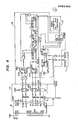
- FIG. 1 a schematic diagram of a first embodiment of an optical reading apparatus according to the present invention is shown.
- the reading apparatus of the invention will be described in connection with a bar code reader which converts bar coded information into electrical signals indicative of figures, letters or the like.
- the reference 1 is a bar code label on which a bar code la having black bars and white bars (light spaces), which are all parallel to each other, are printed as a light and shade pattern.
- Fig. 2 illustrates the bar code label 1 and the head portion of the bar code reader of Fig. 1.
- the reference 2 indicates a casing of a hand-held bar code reader.
- the bar code reader comprises within the casing 2 a light source 3 having a plurality of lamps for illuminating the bar code label 1, and a semi-cylindrical lens 4 for condensing the light from the light source 3 so that the light is incident on the bar code label 1 after being condensed.
- the reference 5 is a reflecting mirror used for reflecting reflected light from the bar code label 1 in a predetermined direction, i.e.
- the reference 9 is a driving circuit for the image sensor 8. Necessary clock pulses for driving the image sensor 8 are produced by the driving circuit 9 by changing clock pulses from a clock generator 18, and are applied to the image sensor 8.
- the reference 10 is an analog amplifier which amplifies an output electrical signal from the image sensor 8, obtained by scanning.
- the reference 11 is a waveform shaping circuit for shaping the waveform of the output signal from the analog amplifire 10, and this waveform shaping circuit 11 comprises a sample-and-hold circuit for converting the output signal into a continuous signal and a low pass filter for smoothing the output signal waveform.
- the reference 12 is a comparator for converting the waveform shaped signal from the waveform shaping circuit 11 into a binary signal having high and low levels respectively corresponding to the black and white bars.
- the reference 13 is an inversion detecting circuit, which sends a latch pulse and clear pulse retarded slightly from the latch pulse to a latch 15 and a counter 14 each time of inversion, i.e.
- the reference 17 is a first clock generator for generating two basic clock pulse trains each having a predetermined frequency.
- the counter 14 repeats counting the number of pulses of one of the basic clocks each time it is cleared in response to the clear pulse from the inversion detecting circuit 13, and its count indicates a value corresponding to the width of each bar of the bar code la.
- the latch 15 stores therein the counts of the counter 14, i.e. the width of each bar, which is obtained just before the counter 14 is cleared.
- the clock generator 18, which will be referred to as a second clock generator, is responsive to the first clock generator 17 so that the former produces clock pulse trains necessary for driving the image sensor 8, and two timing clock pulse trains which are respectively necessary for the sample-and-hold circuit in the waveform shaping circuit 11.
- a microcomputer 16 having a central processing unit (CPU), a random access memory (RAM), a read-only memory (ROM), and an input-output device (I/O) is provided to decode the output information from the latch 15 so as to detect the width of each bar.
- a piezo-electric buzzer 19 is provided to the casing 1 of the hand-held bar code reader to inform the operator of the completion of reading. Namely, the piezo-electric buzzer 19 is responsive to an output signal from the microcomputer 16, which is emitted when the width of all the bars is detected.
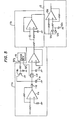
- Fig. 3 is a circuit diagram of the image sensor 8 shown in Fig. 1.
- the image sensor 8 functioning as a transducer is of a charge-coupled device (CCD) type which formed in an LSI chip as shown in Fig. 4.
- the image sensor 8 comprises an array of optical imaging elements or photodiodes 8a, a pair of transfer gates 8bl and 8b2, a pair of shift registers 8cl and 8c2, an output gate 8d, a reset gate 8e, and an FET 8f.
- the photodiode array 8a receives the light from the lens 6 so that an image of a received bar code is converted into an electrical signal by producing a plurality of signal charges in each capacitor of each photodiode.
- the plurality of photodiodes in the array 8a are ectrically divided into two groups.
- the first group includes photodiodes of odd number
- the second group includes photodiodes of even number.
- odd and even numbers respectively mean the order of the photodiodes numbered from one end of the array.
- the first transfer gate 8bl is responsive to the first group photodiodes
- the second transfer gate 8b2 is responsive to the second group photodiodes.
- the first and second transfer gate 8bl and 8b2 are respectively responsive to the output signals or signal charges from photodiodes which are alternately arranged.
- the first and second transfer gates 8bl and 8b2 are respectively driven by first and second transfer gate clocks ⁇ TG1 and ⁇ TG2 .
- the first and second shift registers 8cl and 8c2 are respectively responsive to the output signals from the first and second transfer gates 8bl and 8b2. Namely, signal charges from the odd photodiodes are fed via the first transfer gate 8bl to the first shift register 8cl, while signal charges from the even photodiodes are fed via the second transfer gate 8b2 to the second shift register 8c2.
- the first and second shift registers 8cl and 8c2 are respectively driven by first and second shift register clocks ⁇ 1 and ⁇ 2 so that signals temporarily stored in each shift register are derived out one after another in response to pulses of corresponding clocks.
- the output signals from the first and second shift registers 8cl and 8c2 are both fed to the output gate 8d in which these two output signals are combined to produce a single output.
- the reset gate 8e is driven by a clock pulse train ⁇ RS so that the amplitude of the output signal from the output gate 8d is periodically fixed to a voltage at the drain of the FET 8f.
- the drain-source path of the F E T 8e is interposed between a power supply V DD and ground.
- the output terminal of the image sensor 8 is designated at the reference OS..
- Fig. 4 is a circuit diagram showing a detailed structure of the driving circuit 9, and the first and second clock generators 17 and 18.
- the second clock generator 18 is responsive to clock pulses from the first clock generator 17 so that various clock pulses are produced by counting and processing the basic clock, and these various clock signals produced by the second clock generator 18 are applied via the driving circuit 9 to the image sensor 8 as scanning signals. Furthermore, the second clock generator 18 produces another clock or control signal which is applied to the sample-and-hold circuit of the waveform shaping circuit 11. This control signal is synchronized with the scanning signal, and is used to convert discrete signals into a continuous signal.
- Fig. 5 is a detailed circuit diagram of the waveform shaping circuit 11, and the comparator 12.
- the waveform shaping circuit 11 comprises the sample-and-hold circuit lla and the low pass filter llb as described in the above so that discrete signals are converted into a continuous signal, while harmonic noises are removed when shaping the waveform.
- the comparator 12 produces pulse signals indicative of black and while bars.
- the bar code reader having the structure described in the above operates as follows.
- the head portion of the hand-held bar code reader is directed at the bar code label 1 as shown in Fig. 2 with the light source 3 being energized.
- the light rays from the light source 3 is condensed by the lens 4 to illuminate the bar code label 1 so that the intensity of light reflected at black bars is lower than that of reflected light from white bars.
- the reflected light is transmitted through the reflecting mirror 5, the lens 6 and the diaphragm member 7 so that the pattern of the bar code la is imaged on a scanning line on the image sensor 8.
- the focal depth is made sufficiently deep to avoide unfocussing, and a sufficient amount of light can pass therethrough to ensure accurate reading by the image sensor 8.
- the image sensor 8 performs electronic scanning in receipt of clock pulse signals from the driving circuit 9 so that the black and white bars imaged on the scanning line thereof are converted into corresponding electrical signals.
- the clock pulses from the driving circuit 9 are repeatedly fed to the image sensor 8 so that electronic scanning is repeatedly effected until reading is completed.
- the output electrical signal from the image sensor 8 is amplified by the analog amplifier 10, and then fed to the waveform shapig circuit 11.
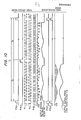
- first and second transfer gate clocks ⁇ TG1 and ⁇ TG2 are shown to appear alternately at a period of T 2 or T 3 . This means that odd signal charges and even signal charges are respectively derived from the photodiode array 8a at different timings.
- waveforms of the first and second transfer gate clocks ⁇ TG1 and $TG2 are shown waveforms of the first and second shift register clocks ⁇ 1 and 0 2 by which the signal charges are respectively fed from the first and second shift registers 8cl and 8c2 to the output gate 8d.
- ⁇ 1 and ⁇ 2 is shown a waveform of the reset pulse ⁇ RS by which the reset gate 8e is turned on and off to derive the output signal from the output gate 8d.
- the first transfer gate 8bl is made open in response to the first transfer gate pulse ⁇ TG1 so that odd signal charges stored in capacitances of odd photodiodes are all transferred to the first shift register at once. Then the odd signal charges are transferred one after another to the output gate 8d in response to the first shift register clock ⁇ 1 and the reset pulse ⁇ RS At this time the second transfer gate 8b2 is closed, and therefore, even signal charges are still stored in the capacitors of the even photodiodes. As a result, only the odd signal charges are derived one after another during a period of time T 2 .
- the second transfer gate clock ⁇ TG2 is applied to the second tranfer gate 8b2 to open the same.
- the siganl charges in the second shift register 8c2 are fed to the output gate 8d one after another within a period of time T3 whose length is equal to that of T 2 in this embodiment. The above operations are repeated so that continuous scanning is performed.
- the storing time of the odd signal charges is equal to the interval between two consecutive pulses of the first transfer gate clock ⁇ TG1' and the storing time of the even signal charges equals the interval between two consecutive pulses of the second transfer gate clock ⁇ TG2 .
- This interval is twice T 2 or T 2 + T 3 , and is expressed in terms of T l .
- the storing time can be made twice the reading cycle in which the signal charges indicative of black and white bars are decoded. This means that if the reading cycle is set constant; the charging or storing time can be doubled when compared with a case in which the stored signal charges of all photodiodes are derived at once. This doubled storing time results in increase in sensitivity in double.
- the output signal obtained at the output terminal OS of the image sensor 8 is shown below the waveform of the reset pulse ⁇ RS' and is applied to the analog amplifier 10 to be amplified therein, and then the amplified output signal is fed to the waveform shaping circuit 11.
- the sample-and-hold circuit lla of the waveform shaping circuit 11 is responsive to the output signal from the reading sensor 8 so that discrete signals, which are synchonized with the shift clock ⁇ 1 or ⁇ 2' are converted into a continuous signal by sampling and holding the output signal from the image sensor 8 at the timing of the sampling clocks SP 1 and SP 2 fed from the second clock generator 18.
- the sample-and-hold circuit lla comprises an inverting amplifier llc which inverts the discrete output signals from the image sensor 8, a diode lld and a capacitor lle which hold a peak value of the output signal from the inverting amlplifier llc.
- An analog switch llf performs on-off operation in response to pulses of the first sampling clock S P1 from the second.clock generator 18 so that the peak value stored in the capacitor. 11e is intermittently transmitted to another capacitor llg.
- the peak voltage is transmitted to the capacitor llg in which it is stored until an instant of subsequent sampling.
- the reference llh is a transistor adapted to discharge the capacitor lie after the analog switch 11f opens with the - peak voltage across the capacitor lle being transmitted to the capacitor llg, in synchronizm with pulses of the second sampling clock SP 2 so that the capacitor lie is prepared to holding operation on next sampling.
- Fig. 7 illustrates the timing of the sampling clock pulses SP 1 and SP 2 with respect to the shift register clocks and ⁇ 2 .
- a first sampling pulse SP 1 is fed to the analog switch llf to close the same so that the peak value of the video signal is transmitted therethrough to the capacitor llg.
- a second sampling pulse SP 2 is fed to the transistor llh so that peak voltage stored in the capacitor lle is discharged. It will be understood that these first and second sampling clocks SP 1 and SP 2 are synchronized with the shift register clocks ⁇ 1 and ⁇ 2 .
- the reference llb is a low pass filter which extracts low frequency components from the output signal of the sample-and-hold circuit lla.
- the cutoff frequency of the low pass filter llb is set to a value which is lower than the frequency of the continuous signal corresponding to a wide bar of the bar code la, from the sample-and-hold circuit lla. With the provision of the low pass filter llb, noise componets etc are removed from the continuous signal.
- the downmost waveform in Fig. 6 shows the continuous signal passed through the low pass filter llb.
- the waveform shaping circuit 11 comprises the above-mentioned sample-and-hold circuit lla and the low pass filter llb so that the output video signal in the form of discrete signals, is shaped to be a continuous analog signal.
- the output signal from the low pass filter llb of the waveform shaping circuit 11 is applied to the comparator 12 which converts the analog signal into a binary signal of high and low levels corresponding to the black bars and white bars.
- the references 12a and 12b are inverse-parallel connected diodes, 12c a capacitor both connected to a noninverting input terminal of an operational amplifier 12d. Namely, the amplitude of the input signal is reduced by the forward voltage drop of the diodes 12a and 12b, while the phase of the input signal is shifted by the capacitor 12c to provide a reference signal for the comparison with the input signal.
- the operational amplifier 12d compares the output signal from the low pass filter llb with the reference signal to obtain a bianary signal at its output.
- the binary signal corresponding to the black and white bars is used to derive data indicative of the width of each bar in the following circuits shown in Fig. 1. Namely, the width of each pulse in the binary signal is measured by counting the number of clock pulses by the counter 14 so as to produce data indicative of the width of each bar. This data is read by the microcomputer 16 so that predetermined operation is executed to complete reading of the bar code la.
- T 2 is not required to be equal to T 3 .
- T 2 and T 3 may be selected so that each of the odd and even signal charges can be read out from the corresponding shift registers 8cl and 8c2 within these periods of time T 2 and T 3 respectively.
- odd and even signal charges can be stored in the photodiode array for T 1 which equals the sum of T 2 and T 3 .
- the charging time is made longer than the reading time for each group of the optical imaging elements 8a, high sensitivity is obtained which contributes to stable converting operation for producing binary signals indicative of light and shade bars.
- optical imaging elements of the two groups are respectively and alternately driven or scanned, undesirable influence due to variations in characteristics of each imaging element can be reduced. Namely, signal variations due to such characteristic variation does not affect the reading operation.
- a transfer gate clock control circuit 19 is added as shown in Fig. 8. Namely, the transfer gate clock control circuit 19 is responsive to a clock from the second clock generator 18 and to a command signal from the microcomputer 16 so that the image sensor 8 is driven in two different ways as will be described hereinbelow.
- Fig. 9 shows a detailed circuit diagram of the transfer gate clock control circuit 19 of Fig. 8.
- the structure of the image sensor 8 as well as other circuits used in the second embodiment is substantially the same as that of the first embodiment, and therefore description thereof is omitted.
- the reference TCS in Fig. 9 indicates a transfer gate clock control signal fed from the microcomputer 16 to the transfer gate clock control circuit 19.
- the control signal TCS is arranged to assume one of high and low levels to control the transfer gate clock control circuit 19 so as to produce two kinds of output clock signals which are fed to the sensor driving circuit 9.
- What is intended by the second embodiment is to switch the image sensor 8 so that one of high-speed and low-speed operations is selected.
- the reading time T2 equals T3
- the reading time'T2, T3 is one half the charge storing time Tl, providing two read data within the charging time Tl. Therefore, high-speed signal processing can be attained.
- increase in reading speed necessarily results in deterioration in resolving power.
- the first embodiment reading apparatus satisfactorily operates at a high speed.
- it is desirable that the resolving power can be increased with the reading speed reduced.
- the second embodiment has been provided so that it is possible to select one of high-speed, low-resolving power mode and low-speed, high-resolving power mode is selected.
- the control signal TCS is produced by the microcomputer 16. Namely, above selection is automatically effected by detecting the result of signal processing as will be described later. However, if desired, this selection between the two modes may be manually controlled.
- the odd and even signal charges in the optical imaging elements or photodiodes 8a are simultanuously derived to be tranferred to the first and second transfer gates 8bl and 8b2 of Fig. 3, and the signal charges in the first and second transfer gates 8bl and 8b2 are simultaneously transferred to the first and second shift registers 8cl and 8c2 respectively.
- the first and second shift registers 8cl and 8c2 are driven by the shift register clocks ⁇ 1 and ⁇ 2 , and therefore, odd and even signal charges are respectively fed to the output gate 8e one after another. Therefore, the output signal at the output terminal OS shows a frequency which is twice the frequency of the output signal obtained with ⁇ TG1 and ⁇ TG2 .
- the resolving power is increased as much as the increase in frequency.
- the charge storing time Tl is the same as that of high-speed reading, and therefore, an adequate sensitively is also ensured.
- the high-resolving power mode is selected, the number of output data obtained during the period Tl is only one whereas the number of data obtained in high-speed mode is two.
- the high-resolving power mode requires a duration expressed by 4T1.
- the high-speed mode requires a duration of 2T1 to the same end. Namely, the high-resolving power mode needs twice the reading time of the high-speed mode.
- Fig. 11 is a timing chart showing the relationship between the first and second shift register clocks 1 and 2 and the above-mentioned first and second sampling clocks SP 1 and SP 2 .
- Wavefors denoted by ⁇ 1 , ⁇ 2 , SP 1 and SP 2 are substantially the same as those of Fig. 7 illustrating the opeation of the first embodiment. Namely, when high-speed mode is selected when using the second embodiment reader, samping and holding operations are performed in the same way as in the first embodiment. However, when the high-resolving power mode is selected, the waveforms of the first and second sampling clocks SP 1 and S P2 are changed as indicated by the references SP 1 , and SP 2 ,. Namely, the frequency of these sampling clocks is doubled.
- Fig. 9 does not show circuitry for producing the first and second sampling clocks SP 11 SP 21 SP 1' and SP 2 ', the circuitry of the second clock generator of Fig. 4 may be modified so that the frequency of the first and second sampling clocks is changed to high in response to the high level transfer gate clock control signal TSC applied to the transfer gate clock control circuit 19.
- the above-mentioned high-speed mode and high-resolving power mode are automatically selected as described in the above.
- the microcomputer 16 usually produces a low level TCS signal.
- the image sensor 8 is put in high-speed mode.
- the microcomputer 16 detects the width of each bar from the information from the latch 15 as described in connection with Fig. 1, and further detects if the width measured is equal to or greater than a predetermined value. If the width of a detected bar is narrower than the predetermined width, it is regarded that the resolving power of the image sensor 8 is insufficient. Then the microcomputer 16 turns the control signal TCS to high level.
- the transfer gate clock control circuit 19 receives the high level control signal TCS so that the image sensor 8 is put in high-resolving power mode.
- the transfer gate clocks ⁇ TG' and ⁇ TG2' are respectively applied to the transfer gates 8bl and 8bc. If desired, however, the selection between high-speed mode and high-resolving power mode may be manually effected with a suitable manual switch provided to produce the control signal of high or low level.
- the reading sensor 8 of one-dimentional or linear type is employed, the present invention is not limited to such a linear image sensor. Namely, the present invention may be adapted to a two-dimentional or area image sensor.
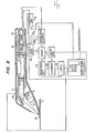
- Fig. 12 shows an optical reader adapted to read or recognize figures or characters lb printed on a label 1.
- the optical reader of Fig. 12 comprises, therefore, a two-dimentional image sensor 8' which converts a two-dimentional image information 2a imaged thereon into an electrical signal by electronically scanning the image 2a.
- the two-dimentional image sensor 8' comprises a plurality of arrays of optical imaging elements of charge transfer device type. Therefore, the optical imaging elements on each array are divided into two groups as described in connection with the first and second embodiments so that each group can be driven in the same manner as in the first or second embodiment.
- similar effects to the first and second embodiments may be obtained with such a two-dimentional image sensor 8'.
- a single optical imaging element array may be divided into more than two groups with more than two shift registers employed. Namely, signal charges in respective groups may be derived one after another. Namely, when high resolving power is not required because of sufficient thickness or width of optical information, the number of groups may be increased to more than two. Such increase in the number of groups results in increase in speed in reading operation because more than two read data can be obtained within the aforementioned time period Tl .
- optical imaging elements of each group are equidistantly arranged.
Abstract
Description
- This invention relates generally to optical reading apparatus, such as a bar code reader, arranged to read coded information, characters or the like by an image sensor of electronic scanning type, and to a method of reading such optically readable information.
- Among various types of optical reading apparatus a bar code reader using a charge transfer device imager or image sensor is known. When a charge transfer device image sensor is used as a transducer, a problem occurs that the output signal level from the image sensor would be low as the reading speed is increased. Namely, high-speed reading necessarily results in a short charge storage time which turns to insufficiently low output signal level, resulting in low sensitivity.
- In order to increase the level of the output signal from such a charge transfer device image sensor, the intensity of incident light may be increased. However, this results in various problems, such as the increase in space occupied by the light source, power consumption and generated heat. Therefore, the intensity of incident light cannot be increased so much.
- The present invention has been developed in order to remove the above-described drawbacks inherent to the conventional optical reading apparatus.
- It is, therefore, an object of the present invention to provide an optical reading apparatus and a method of optically reading information, with which sufficient sensitivity is ensured even in high-speed reading.
- According to a feature of the present invention a plurality of optical imaging elements arranged in an array, which are electrically divided in two or more groups, are respectively driven by different timing clocks so that signal charges from respective groups are derived at differnt timings. Although the frequency of each of the timing clocks is set to a value so that sufficient length of charging time is provided to increase'the sensitivity, two or more reading data can be obtained within one cycle of charging period, resulting in increase in reading speed. In one embodiment, the operating mode of the reading apparatus may be switched to either high-speed mode or high-resolution mode.
- In accordance with the present invention, there is provided an optical reading apparatus for converting optically readable information into an electrical signal, comprising: a charge transfer device image sensor for converting optical information into an electrical signal, the image sensor having a plurality of optical imaging elements arranged in an array, the optical imaging elements being electrically divided into two or more groups so that signal charges from one group can be derived simultaneously, the image sensor having an output circuit responsive to a plurality of electrical signals each produced by each of the two or more groups so that the plurality of electrical signals are combined as a single output signal; means for driving the image sensor so that the image sensor performs electronic scanning by deriving signal charges from the optical imaging elements; and means responsive to the output signal from the image sensor for processing the same to produce an electrical signal indicative of the read information, characterized in that the driving means produces at least two clocks which are shifted by an amount of time from each other, the at least two clocks being fed to the image sensor in such a manner that at least two groups of the optical imaging elements are driven alternately.
- In accordance with the present invention, there is also provided an optical reading apparatus for converting optically readable information into an electrical signal, comprising: a charge transfer device image sensor for converting optical information into an electrical signal, the image sensor having a plurality of optical imaging elements arranged in an array, the optical imaging elements being electrically divided into two or more groups so that signal charges from one group can be derived simultaneously, the image sensor having an output circuit responsive to a plurality of electrical signals each produced by each of the two or more groups so that the plurality of electrical signals are combined as a single output signal; means for driving the image sensor so that the image sensor performs electronic scanning by deriving signal charges from the optical imaging element, sthe means producing at least two clocks which are fed to the image sensor so that at least two groups of the optical imaging elements are driven; and means responsive to the output signal from the image sensor for processing the same to produce an electrical signal indicative of the read information, characterized by means for controlling the means for driving so that the at least two clocks have one of first and second time relationships therebetween, the at least two clocks being shifted by an amount of time from each other when in the first time relationship, and the at least two clocks being of the same timing when in the second time relationship, the two clocks having the first time relationship therebetween causing the image sensor to derive signal charges of one group after signal charges of another group have been derived, and the two clocks having the second relationship therebetween causing the image sensor to derive signal charges of all groups simultaneously.
- In accordance with the present invention, there is further provided a method of optically reading optically readable information by means of a charge transfer device image sensor for converting optical information into an electrical signal, the image sensor having a plurality of optical imaging elements arranged in an array, the optical imaging elements being electrically divided into two or more groups so that signal charges from one group can be derived simultaneously, the image sensor having an output circuit responsive to a plurality of electrical signals each produced by each of the two or more groups so that the plurality of electrical signals are combined as a single output signal, characterized by the steps of: causing the optical imaging elements to deliver output signals therefrom so that one group of the optical imaging elements deliver signal charges after another group has delivered signal charges; deriving the signal charges of one group one after another so as to process corresponding electrical signals to detect optical information; and repeating the above steps with respect to each group of the optical imaging elements.
- The object and features of the present invention will become more readily apparent from the following detailed description of the preferred embodiments taken in conjunction with the accompanying drawings in which:
- Fig. 1 is a schematic diagram of an embodiment of an optical reading apparatus according to the present invention;
- Fig. 2 is a schematic view showing the application of the reading apparatus of Fig. 1 as a bar code reader;
- Fig. 3 is a schematic circuit diagram showing the image sensor used in the apparatus of Fig. 1;
- Fig. 4 is a circuit diagram showing circuitry for driving the image sensor of Fig. 1;
- Fig. 5 is a circuit diagram showing circuitry which processes an electrical output signal from the image sensor of Fig. 1;
- Fig. 6 is a timing chart useful for understanding the operation of the embodiment of Figs. 1 through 5;
- Fig. 7 is another timing chart also useful for understanding the operation of the embodiment of Figs. 1 through 5;
- Fig. 8 is a schematic diagram of a second embodiment of an optical reading apparatus according to the present invention;
- Fig. 9 is a circuit diagram showing circuitry for driving the image sensor of Fig. 8;
- Fig. 10 is a timing chart useful for understanding the operation of the second embodiment of Figs. 8 and 9;
- Fig. 11 is another timing chart also useful for understanding the operation of the second embodiment; and
- Fig. 12 is a schematic perspective view of a third embodiment optical reading apparatus according to the present invention.
- The same or corresponding elements and parts are designated at like reference numerals throughout the drawings.
- Referring now to Fig. 1, a schematic diagram of a first embodiment of an optical reading apparatus according to the present invention is shown. The reading apparatus of the invention will be described in connection with a bar code reader which converts bar coded information into electrical signals indicative of figures, letters or the like. The
reference 1 is a bar code label on which a bar code la having black bars and white bars (light spaces), which are all parallel to each other, are printed as a light and shade pattern. - Fig. 2 illustrates the
bar code label 1 and the head portion of the bar code reader of Fig. 1. Turning back to Fig. 1, thereference 2 indicates a casing of a hand-held bar code reader. The bar code reader comprises within thecasing 2 alight source 3 having a plurality of lamps for illuminating thebar code label 1, and asemi-cylindrical lens 4 for condensing the light from thelight source 3 so that the light is incident on thebar code label 1 after being condensed. The reference 5 is a reflecting mirror used for reflecting reflected light from thebar code label 1 in a predetermined direction, i.e. a direction toward animage sensor 8, and the reflected light from the reflecting mirror 5 is transmitted through acondenser lens 6 and adiaphragm member 7 having an elongate slit arranged.so that its longitudinal direction is perpendicular to the reading direction which is normal to the parallel bars, to theimage sensor 8 where an image of the bar code la to be scanned is imaged thereon. Theimage sensor 8 uses a one-dimentional or linear image sensor which converts the image on the scanning line into an electrical signal by electronic scanning operation. A dot-dash line in Fig. 1 indicates the locus of light in the optical system. Thereference 9 is a driving circuit for theimage sensor 8. Necessary clock pulses for driving theimage sensor 8 are produced by thedriving circuit 9 by changing clock pulses from aclock generator 18, and are applied to theimage sensor 8. - The
reference 10 is an analog amplifier which amplifies an output electrical signal from theimage sensor 8, obtained by scanning. Thereference 11 is a waveform shaping circuit for shaping the waveform of the output signal from theanalog amplifire 10, and thiswaveform shaping circuit 11 comprises a sample-and-hold circuit for converting the output signal into a continuous signal and a low pass filter for smoothing the output signal waveform. Thereference 12 is a comparator for converting the waveform shaped signal from thewaveform shaping circuit 11 into a binary signal having high and low levels respectively corresponding to the black and white bars. Thereference 13 is an inversion detecting circuit, which sends a latch pulse and clear pulse retarded slightly from the latch pulse to alatch 15 and acounter 14 each time of inversion, i.e. the instants of rising and falling of the binary signal are detected. Thereference 17 is a first clock generator for generating two basic clock pulse trains each having a predetermined frequency. Thecounter 14 repeats counting the number of pulses of one of the basic clocks each time it is cleared in response to the clear pulse from theinversion detecting circuit 13, and its count indicates a value corresponding to the width of each bar of the bar code la. Thelatch 15 stores therein the counts of thecounter 14, i.e. the width of each bar, which is obtained just before thecounter 14 is cleared. Theclock generator 18, which will be referred to as a second clock generator, is responsive to thefirst clock generator 17 so that the former produces clock pulse trains necessary for driving theimage sensor 8, and two timing clock pulse trains which are respectively necessary for the sample-and-hold circuit in thewaveform shaping circuit 11. - A
microcomputer 16 having a central processing unit (CPU), a random access memory (RAM), a read-only memory (ROM), and an input-output device (I/O) is provided to decode the output information from thelatch 15 so as to detect the width of each bar. A piezo-electric buzzer 19 is provided to thecasing 1 of the hand-held bar code reader to inform the operator of the completion of reading. Namely, the piezo-electric buzzer 19 is responsive to an output signal from themicrocomputer 16, which is emitted when the width of all the bars is detected. - Fig. 3 is a circuit diagram of the
image sensor 8 shown in Fig. 1. Theimage sensor 8 functioning as a transducer is of a charge-coupled device (CCD) type which formed in an LSI chip as shown in Fig. 4. Theimage sensor 8, comprises an array of optical imaging elements orphotodiodes 8a, a pair of transfer gates 8bl and 8b2, a pair of shift registers 8cl and 8c2, anoutput gate 8d, areset gate 8e, and anFET 8f. Thephotodiode array 8a receives the light from thelens 6 so that an image of a received bar code is converted into an electrical signal by producing a plurality of signal charges in each capacitor of each photodiode. The plurality of photodiodes in thearray 8a are ectrically divided into two groups. The first group includes photodiodes of odd number, and the second group includes photodiodes of even number. The words, odd and even numbers respectively mean the order of the photodiodes numbered from one end of the array. The first transfer gate 8bl is responsive to the first group photodiodes, while the second transfer gate 8b2 is responsive to the second group photodiodes. In other words, the first and second transfer gate 8bl and 8b2 are respectively responsive to the output signals or signal charges from photodiodes which are alternately arranged. - The first and second transfer gates 8bl and 8b2 are respectively driven by first and second transfer gate clocks φTG1 and φTG2. The first and second shift registers 8cl and 8c2 are respectively responsive to the output signals from the first and second transfer gates 8bl and 8b2. Namely, signal charges from the odd photodiodes are fed via the first transfer gate 8bl to the first shift register 8cl, while signal charges from the even photodiodes are fed via the second transfer gate 8b2 to the second shift register 8c2. The first and second shift registers 8cl and 8c2 are respectively driven by first and second shift register clocks φ1 and φ2 so that signals temporarily stored in each shift register are derived out one after another in response to pulses of corresponding clocks. The output signals from the first and second shift registers 8cl and 8c2 are both fed to the
output gate 8d in which these two output signals are combined to produce a single output. Thereset gate 8e is driven by a clock pulse train φRS so that the amplitude of the output signal from theoutput gate 8d is periodically fixed to a voltage at the drain of theFET 8f. The drain-source path of the FE T 8e is interposed between a power supply VDD and ground. The output terminal of theimage sensor 8 is designated at the reference OS.. - Fig. 4 is a circuit diagram showing a detailed structure of the driving
circuit 9, and the first andsecond clock generators second clock generator 18 is responsive to clock pulses from thefirst clock generator 17 so that various clock pulses are produced by counting and processing the basic clock, and these various clock signals produced by thesecond clock generator 18 are applied via thedriving circuit 9 to theimage sensor 8 as scanning signals. Furthermore, thesecond clock generator 18 produces another clock or control signal which is applied to the sample-and-hold circuit of thewaveform shaping circuit 11. This control signal is synchronized with the scanning signal, and is used to convert discrete signals into a continuous signal. - Fig. 5 is a detailed circuit diagram of the
waveform shaping circuit 11, and thecomparator 12. Thewaveform shaping circuit 11 comprises the sample-and-hold circuit lla and the low pass filter llb as described in the above so that discrete signals are converted into a continuous signal, while harmonic noises are removed when shaping the waveform. Thecomparator 12 produces pulse signals indicative of black and while bars. - The bar code reader having the structure described in the above operates as follows. In order to read a bar code la printed on the
bar code label 1, the head portion of the hand-held bar code reader is directed at thebar code label 1 as shown in Fig. 2 with thelight source 3 being energized. The light rays from thelight source 3 is condensed by thelens 4 to illuminate thebar code label 1 so that the intensity of light reflected at black bars is lower than that of reflected light from white bars. The reflected light is transmitted through the reflecting mirror 5, thelens 6 and thediaphragm member 7 so that the pattern of the bar code la is imaged on a scanning line on theimage sensor 8. Since the elongate slit made in thediaphragm member 7 is perpendicular to the reading line, the focal depth is made sufficiently deep to avoide unfocussing, and a sufficient amount of light can pass therethrough to ensure accurate reading by theimage sensor 8. - The
image sensor 8 performs electronic scanning in receipt of clock pulse signals from the drivingcircuit 9 so that the black and white bars imaged on the scanning line thereof are converted into corresponding electrical signals. The clock pulses from the drivingcircuit 9 are repeatedly fed to theimage sensor 8 so that electronic scanning is repeatedly effected until reading is completed. The output electrical signal from theimage sensor 8 is amplified by theanalog amplifier 10, and then fed to thewaveform shapig circuit 11. - Now the operation of the
image sensor 8 will be described with reference to timing chart of Fig. 6. The aforementioned first and second transfer gate clocks φTG1 and φTG2 are shown to appear alternately at a period of T2 or T3. This means that odd signal charges and even signal charges are respectively derived from thephotodiode array 8a at different timings. Below the waveforms of the first and second transfer gate clocks φTG1 and $TG2 are shown waveforms of the first and second shift register clocks φ1 and 02 by which the signal charges are respectively fed from the first and second shift registers 8cl and 8c2 to theoutput gate 8d. Below φ1 and φ2 is shown a waveform of the reset pulse φRS by which thereset gate 8e is turned on and off to derive the output signal from theoutput gate 8d. - Describing the operation of the
image sensor 8 in further detail, when the above-mentioned clocks of Fig. 6 are applied to theimage sensor 8, the first transfer gate 8bl is made open in response to the first transfer gate pulse φTG1 so that odd signal charges stored in capacitances of odd photodiodes are all transferred to the first shift register at once. Then the odd signal charges are transferred one after another to theoutput gate 8d in response to the first shift register clock φ1 and the reset pulse φRS At this time the second transfer gate 8b2 is closed, and therefore, even signal charges are still stored in the capacitors of the even photodiodes. As a result, only the odd signal charges are derived one after another during a period of time T2. At the end of the period T2' the second transfer gate clock φTG2 is applied to the second tranfer gate 8b2 to open the same. Thus, even signal charges are transferred to the second shift register 8c2 at once. Then the siganl charges in the second shift register 8c2 are fed to theoutput gate 8d one after another within a period of time T3 whose length is equal to that of T 2 in this embodiment. The above operations are repeated so that continuous scanning is performed. - From the above, it will be understood that the storing time of the odd signal charges is equal to the interval between two consecutive pulses of the first transfer gate clock φTG1' and the storing time of the even signal charges equals the interval between two consecutive pulses of the second transfer gate clock φ TG2. This interval is twice T2 or T2 + T3, and is expressed in terms of Tl. Namely, the storing time can be made twice the reading cycle in which the signal charges indicative of black and white bars are decoded. This means that if the reading cycle is set constant; the charging or storing time can be doubled when compared with a case in which the stored signal charges of all photodiodes are derived at once. This doubled storing time results in increase in sensitivity in double.
- The output signal obtained at the output terminal OS of the
image sensor 8 is shown below the waveform of the reset pulse φRS' and is applied to theanalog amplifier 10 to be amplified therein, and then the amplified output signal is fed to thewaveform shaping circuit 11. - The operation of the
waveform shaping circuit 11 will be described with reference to Fig. 5. The sample-and-hold circuit lla of thewaveform shaping circuit 11 is responsive to the output signal from the readingsensor 8 so that discrete signals, which are synchonized with the shift clock φ1 or φ2' are converted into a continuous signal by sampling and holding the output signal from theimage sensor 8 at the timing of the sampling clocks SP1 and SP2 fed from thesecond clock generator 18. The sample-and-hold circuit lla comprises an inverting amplifier llc which inverts the discrete output signals from theimage sensor 8, a diode lld and a capacitor lle which hold a peak value of the output signal from the inverting amlplifier llc. An analog switch llf performs on-off operation in response to pulses of the first sampling clock SP1 from thesecond.clock generator 18 so that the peak value stored in the capacitor. 11e is intermittently transmitted to another capacitor llg. Thus, the peak voltage is transmitted to the capacitor llg in which it is stored until an instant of subsequent sampling. The reference llh is a transistor adapted to discharge the capacitor lie after theanalog switch 11f opens with the - peak voltage across the capacitor lle being transmitted to the capacitor llg, in synchronizm with pulses of the second sampling clock SP2 so that the capacitor lie is prepared to holding operation on next sampling. - Fig. 7 illustrates the timing of the sampling clock pulses SP1 and SP2 with respect to the shift register clocks and φ2. A first sampling pulse SP1 is fed to the analog switch llf to close the same so that the peak value of the video signal is transmitted therethrough to the capacitor llg. Then a second sampling pulse SP2 is fed to the transistor llh so that peak voltage stored in the capacitor lle is discharged. It will be understood that these first and second sampling clocks SP1 and SP2 are synchronized with the shift register clocks φ1 and φ2.
- The reference llb is a low pass filter which extracts low frequency components from the output signal of the sample-and-hold circuit lla. The cutoff frequency of the low pass filter llb is set to a value which is lower than the frequency of the continuous signal corresponding to a wide bar of the bar code la, from the sample-and-hold circuit lla. With the provision of the low pass filter llb, noise componets etc are removed from the continuous signal. The downmost waveform in Fig. 6 shows the continuous signal passed through the low pass filter llb. The
waveform shaping circuit 11 comprises the above-mentioned sample-and-hold circuit lla and the low pass filter llb so that the output video signal in the form of discrete signals, is shaped to be a continuous analog signal. - The output signal from the low pass filter llb of the
waveform shaping circuit 11 is applied to thecomparator 12 which converts the analog signal into a binary signal of high and low levels corresponding to the black bars and white bars. In thecomparator 12, thereferences 12a and 12b are inverse-parallel connected diodes, 12c a capacitor both connected to a noninverting input terminal of anoperational amplifier 12d. Namely, the amplitude of the input signal is reduced by the forward voltage drop of thediodes 12a and 12b, while the phase of the input signal is shifted by the capacitor 12c to provide a reference signal for the comparison with the input signal. Theoperational amplifier 12d compares the output signal from the low pass filter llb with the reference signal to obtain a bianary signal at its output. The binary signal corresponding to the black and white bars is used to derive data indicative of the width of each bar in the following circuits shown in Fig. 1. Namely, the width of each pulse in the binary signal is measured by counting the number of clock pulses by thecounter 14 so as to produce data indicative of the width of each bar. This data is read by themicrocomputer 16 so that predetermined operation is executed to complete reading of the bar code la. - In the above-described embodiment, although the time interval T2 equals T3 as shown in Fig. 6, T2 is not required to be equal to T3. Namely, T2 and T3 may be selected so that each of the odd and even signal charges can be read out from the corresponding shift registers 8cl and 8c2 within these periods of time T 2 and T3 respectively. Thus, odd and even signal charges can be stored in the photodiode array for T1 which equals the sum of T2 and T3.
- From the above it will be understood that in the above-described embodiment, odd and even signal charges in the optical imaging elements, i.e. the
photodiodes 8a, are separately and alternately derived at different timings so that it is possible to provide a charge storing time which is twice the reading time. This results in increase in sensitivity as described in the above. Moreover, this improves S/N of the output signal from theimage sensor 8. In other words, the amplitude of the electrical sigals corresponding to each bar can vary throughout a larger range. Thus, it is possible to accurately detect white and black bars with these bars being accurately converted into corresponding binary signals. Such accurate conversion provides stable reading operation. Generally speaking, a plurality of read data are usually necessary to determin the read information with high accuracy. Therefore, in the above-described emobodiment, since two pieces of read data can be obtained within one cycle of charging period Tl, a high-speed reading may be achieved. - Moreover, since the charging time is made longer than the reading time for each group of the
optical imaging elements 8a, high sensitivity is obtained which contributes to stable converting operation for producing binary signals indicative of light and shade bars. Furthermore, optical imaging elements of the two groups are respectively and alternately driven or scanned, undesirable influence due to variations in characteristics of each imaging element can be reduced. Namely, signal variations due to such characteristic variation does not affect the reading operation. - Now a modification of the above-embodiment or second embodiment of the present invention will be described with reference to Figs. 8 through 11. This embodiment differs from the above-described first embodiment in that a transfer gate
clock control circuit 19 is added as shown in Fig. 8. Namely, the transfer gateclock control circuit 19 is responsive to a clock from thesecond clock generator 18 and to a command signal from themicrocomputer 16 so that theimage sensor 8 is driven in two different ways as will be described hereinbelow. - Fig. 9 shows a detailed circuit diagram of the transfer gate
clock control circuit 19 of Fig. 8. The structure of theimage sensor 8 as well as other circuits used in the second embodiment is substantially the same as that of the first embodiment, and therefore description thereof is omitted. The reference TCS in Fig. 9 indicates a transfer gate clock control signal fed from themicrocomputer 16 to the transfer gateclock control circuit 19. The control signal TCS is arranged to assume one of high and low levels to control the transfer gateclock control circuit 19 so as to produce two kinds of output clock signals which are fed to thesensor driving circuit 9. - What is intended by the second embodiment is to switch the
image sensor 8 so that one of high-speed and low-speed operations is selected. As described in connection with the first embodiment, if the reading time T2 equals T3, the reading time'T2, T3 is one half the charge storing time Tl, providing two read data within the charging time Tl. Therefore, high-speed signal processing can be attained. However, such increase in reading speed necessarily results in deterioration in resolving power. When high resolving power is not needed, the first embodiment reading apparatus satisfactorily operates at a high speed. However, when high resolving power is required, it is desirable that the resolving power can be increased with the reading speed reduced. The second embodiment has been provided so that it is possible to select one of high-speed, low-resolving power mode and low-speed, high-resolving power mode is selected. In the illustrated second embodiment, the control signal TCS is produced by themicrocomputer 16. Namely, above selection is automatically effected by detecting the result of signal processing as will be described later. However, if desired, this selection between the two modes may be manually controlled. - The operation of the second embodiment of Figs. 8 and 9 will be described in detail with reference to Figs. 10 and 11. When the control sigal TCS applied from the
microcomputer 16 assumes a low level, the first and second transfer gate clocks φTG1 and φTG2 are produced in the same manner as in the first embodiment. Under this condition, the reading apparatus operates as described in connection with the first embodiment. On the other hand, when the control signal TCS is switchd to high level, the timing or phase of the second transfer gate clock φTG2 is changed so that its timing equals that of φTG1 as shown in waveforsm φTG1' and φTG2' in Fig. 10. Therefore, the odd and even signal charges in the optical imaging elements orphotodiodes 8a are simultanuously derived to be tranferred to the first and second transfer gates 8bl and 8b2 of Fig. 3, and the signal charges in the first and second transfer gates 8bl and 8b2 are simultaneously transferred to the first and second shift registers 8cl and 8c2 respectively. The first and second shift registers 8cl and 8c2 are driven by the shift register clocks φ1 and φ2, and therefore, odd and even signal charges are respectively fed to theoutput gate 8e one after another. Therefore, the output signal at the output terminal OS shows a frequency which is twice the frequency of the output signal obtained with φTG1 and φTG2. Accordingly, the resolving power is increased as much as the increase in frequency. The charge storing time Tl is the same as that of high-speed reading, and therefore, an adequate sensitively is also ensured. However, when the high-resolving power mode is selected, the number of output data obtained during the period Tl is only one whereas the number of data obtained in high-speed mode is two. In order to increase the liability of output data, several data are usually necessary as described in the above. Suppose four data are necessary to find coincidence therebetween, the high-resolving power mode requires a duration expressed by 4T1. On the other hand, the high-speed mode requires a duration of 2T1 to the same end. Namely, the high-resolving power mode needs twice the reading time of the high-speed mode. - Fig. 11 is a timing chart showing the relationship between the first and second shift register clocks 1 and 2 and the above-mentioned first and second sampling clocks SP1 and SP2. Wavefors denoted by φ1, φ2, SP1 and SP2 are substantially the same as those of Fig. 7 illustrating the opeation of the first embodiment. Namely, when high-speed mode is selected when using the second embodiment reader, samping and holding operations are performed in the same way as in the first embodiment. However, when the high-resolving power mode is selected, the waveforms of the first and second sampling clocks SP1 and SP2 are changed as indicated by the references SP1, and SP2,. Namely, the frequency of these sampling clocks is doubled. Although Fig. 9 does not show circuitry for producing the first and second sampling clocks SP11 SP21 SP1' and SP2', the circuitry of the second clock generator of Fig. 4 may be modified so that the frequency of the first and second sampling clocks is changed to high in response to the high level transfer gate clock control signal TSC applied to the transfer gate
clock control circuit 19. - The above-mentioned high-speed mode and high-resolving power mode are automatically selected as described in the above. Namely, the
microcomputer 16 usually produces a low level TCS signal. As a result, theimage sensor 8 is put in high-speed mode. Themicrocomputer 16 detects the width of each bar from the information from thelatch 15 as described in connection with Fig. 1, and further detects if the width measured is equal to or greater than a predetermined value. If the width of a detected bar is narrower than the predetermined width, it is regarded that the resolving power of theimage sensor 8 is insufficient. Then themicrocomputer 16 turns the control signal TCS to high level. As a result, the transfer gateclock control circuit 19 receives the high level control signal TCS so that theimage sensor 8 is put in high-resolving power mode. Namely, the transfer gate clocks φTG' and φTG2' are respectively applied to the transfer gates 8bl and 8bc. If desired, however, the selection between high-speed mode and high-resolving power mode may be manually effected with a suitable manual switch provided to produce the control signal of high or low level. - Although the above-described.embodiments are both directed to a bar code reader, and therefore, the reading
sensor 8 of one-dimentional or linear type is employed, the present invention is not limited to such a linear image sensor. Namely, the present invention may be adapted to a two-dimentional or area image sensor. - Hence, reference is now made to Fig. 12 showing a schematic perspective view of a thi-rd embodiment of the present invention. Fig. 12 shows an optical reader adapted to read or recognize figures or characters lb printed on a
label 1. The optical reader of Fig. 12 comprises, therefore, a two-dimentional image sensor 8' which converts a two-dimentional image information 2a imaged thereon into an electrical signal by electronically scanning theimage 2a. The two-dimentional image sensor 8' comprises a plurality of arrays of optical imaging elements of charge transfer device type. Therefore, the optical imaging elements on each array are divided into two groups as described in connection with the first and second embodiments so that each group can be driven in the same manner as in the first or second embodiment. Thus, similar effects to the first and second embodiments may be obtained with such a two-dimentional image sensor 8'. - Although it has been described that the optical imaging elements or photodiodes in the form of an array are divided into two groups so that odd and even signal charges are respectively derived independent of the other, a single optical imaging element array may be divided into more than two groups with more than two shift registers employed. Namely, signal charges in respective groups may be derived one after another. Namely, when high resolving power is not required because of sufficient thickness or width of optical information, the number of groups may be increased to more than two. Such increase in the number of groups results in increase in speed in reading operation because more than two read data can be obtained within the aforementioned time period Tl. When electrically dividing the optical imaging elements of a single array into more than two groups, it is preferable that optical imaging elements of each group are equidistantly arranged.
- The above-described embodiments are just examples of the present invention, and therefore, it will be apparent for those skilled in the art that many modifications and variations may be made without departing from the spirit of the present invention.
Claims (9)
characterized by the steps of: causing the optical imaging elements (8a) to deliver output signals therefrom so that one group of said optical imaging elements (8a) deliver signal charges after another group has delivered signal charges; deriving the signal charges of one group one after another so as to process corresponding electrical signals to detect optical information; and repeating the above steps with respect to each group of said optical imaging elements.
characterized in that the number of said groups is two so that signal charges of odd number and signal charges of even number are respectively derived at different timings, wherein odd and even numbers indicate the position of each optical imaging element viewed from one end of the array (8a).
Applications Claiming Priority (4)
| Application Number | Priority Date | Filing Date | Title |
|---|---|---|---|
| JP814282A JPS58125179A (en) | 1982-01-20 | 1982-01-20 | Method and device for reading of bar code |
| JP8142/82 | 1982-01-20 | ||
| JP169189/82 | 1982-09-28 | ||
| JP57169189A JPS5958582A (en) | 1982-09-28 | 1982-09-28 | Optical information reader |
Publications (3)
| Publication Number | Publication Date |
|---|---|
| EP0085495A2 true EP0085495A2 (en) | 1983-08-10 |
| EP0085495A3 EP0085495A3 (en) | 1984-06-20 |
| EP0085495B1 EP0085495B1 (en) | 1987-09-16 |
Family
ID=26342593
Family Applications (1)
| Application Number | Title | Priority Date | Filing Date |
|---|---|---|---|
| EP83300197A Expired EP0085495B1 (en) | 1982-01-20 | 1983-01-14 | High-sensitive optical reading apparatus and method of reading optical information |
Country Status (3)
| Country | Link |
|---|---|
| US (1) | US4516017A (en) |
| EP (1) | EP0085495B1 (en) |
| DE (1) | DE3373734D1 (en) |
Cited By (7)
| Publication number | Priority date | Publication date | Assignee | Title |
|---|---|---|---|---|
| FR2565746A1 (en) * | 1984-06-06 | 1985-12-13 | Sud Sa Systemes | Method and device for processing an analog electrical signal and application to the reading of bar codes |
| EP0204841A1 (en) * | 1984-12-13 | 1986-12-17 | Veeco Intergrated Automation, Inc. | Static bar code reader |
| EP0221545A2 (en) * | 1985-11-06 | 1987-05-13 | Nippondenso Co., Ltd. | Optical information reading apparatus |
| EP0385478A2 (en) * | 1989-03-01 | 1990-09-05 | Symbol Technologies, Inc. | Bar code reader |
| US5591955A (en) * | 1993-05-11 | 1997-01-07 | Laser; Vadim | Portable data file readers |
| EP0789315A2 (en) * | 1996-02-10 | 1997-08-13 | Datalogic S.P.A. | Method and apparatus for the acquisition of information assigned to objects |
| US5811828A (en) * | 1991-09-17 | 1998-09-22 | Norand Corporation | Portable reader system having an adjustable optical focusing means for reading optical information over a substantial range of distances |
Families Citing this family (30)
| Publication number | Priority date | Publication date | Assignee | Title |
|---|---|---|---|---|
| JPH07107688B2 (en) * | 1986-03-18 | 1995-11-15 | 日本電装株式会社 | Optical information reader |
| US4874933A (en) * | 1987-08-21 | 1989-10-17 | Recognition Equipment Incorporated | Ambient illumination bar code reader |
| US5216523A (en) * | 1989-10-27 | 1993-06-01 | Matsushita Electric Industrial Co., Ltd. | Small data terminal apparatus with CCD image sensor |
| US5552592A (en) * | 1989-10-30 | 1996-09-03 | Symbol Technologies, Inc. | Slim scan module with dual detectors |
| US5654533A (en) * | 1992-10-26 | 1997-08-05 | Kabushiki Kaisha Tec | Apparatus and method for reading two-dimensional symbols |
| JPH06334920A (en) * | 1993-03-23 | 1994-12-02 | Nippon Hoso Kyokai <Nhk> | Solid state image pickup element and driving method thereof |
| US5446271A (en) * | 1993-08-06 | 1995-08-29 | Spectra-Physics Scanning Systems, Inc. | Omnidirectional scanning method and apparatus |
| US5504317A (en) * | 1994-01-05 | 1996-04-02 | Opticon, Inc. | Optical reader |
| DE69515481T2 (en) * | 1994-06-07 | 2000-10-19 | United Parcel Service Inc | Method and device for decoding a two-dimensional symbol in space |
| KR100193372B1 (en) * | 1994-08-22 | 1999-06-15 | 가시오 가즈오 | Handheld scanner |
| JPH09288712A (en) * | 1996-04-19 | 1997-11-04 | Matsushita Electric Ind Co Ltd | Bar code reader |
| JPH11184960A (en) * | 1997-10-16 | 1999-07-09 | Tohoku Ricoh Co Ltd | Bar code reader |
| US6119939A (en) * | 1998-07-08 | 2000-09-19 | Welch Allyn, Inc. | Optical assembly for barcode scanner |
| US6275388B1 (en) * | 1998-07-08 | 2001-08-14 | Welch Allyn Data Collection, Inc. | Image sensor mounting system |
| US6164544A (en) * | 1998-07-08 | 2000-12-26 | Welch Allyn Data Collection, Inc. | Adjustable illumination system for a barcode scanner |
| US6728391B1 (en) | 1999-12-03 | 2004-04-27 | United Parcel Service Of America, Inc. | Multi-resolution label locator |
| US20020036234A1 (en) * | 2000-03-31 | 2002-03-28 | Hong Tang | Spectral data collector which includes a lambertian reflector |
| US6775077B1 (en) * | 2000-09-22 | 2004-08-10 | Symbol Technologies, Inc. | Micro reader scan engine with prism |
| US6637657B2 (en) | 2001-04-06 | 2003-10-28 | Symbol Technologies, Inc. | Compact scan module with magnetically centered scan mirror |
| US6834807B2 (en) | 2001-07-13 | 2004-12-28 | Hand Held Products, Inc. | Optical reader having a color imager |
| US6935564B2 (en) * | 2001-07-30 | 2005-08-30 | Bayer Healthcare Llc | Circuit and method for correcting influence of AC coupling |
| EP1437676B1 (en) * | 2002-12-31 | 2007-10-24 | Datalogic S.P.A. | Method for reading a graphic pattern and acquiring its image |
| US7780089B2 (en) * | 2005-06-03 | 2010-08-24 | Hand Held Products, Inc. | Digital picture taking optical reader having hybrid monochrome and color image sensor array |
| US7611060B2 (en) | 2005-03-11 | 2009-11-03 | Hand Held Products, Inc. | System and method to automatically focus an image reader |
| US7568628B2 (en) | 2005-03-11 | 2009-08-04 | Hand Held Products, Inc. | Bar code reading device with global electronic shutter control |
| US7770799B2 (en) | 2005-06-03 | 2010-08-10 | Hand Held Products, Inc. | Optical reader having reduced specular reflection read failures |
| US20100316291A1 (en) * | 2009-06-11 | 2010-12-16 | Shulan Deng | Imaging terminal having data compression |
| US20110080500A1 (en) * | 2009-10-05 | 2011-04-07 | Hand Held Products, Inc. | Imaging terminal, imaging sensor having multiple reset and/or multiple read mode and methods for operating the same |
| US8657200B2 (en) | 2011-06-20 | 2014-02-25 | Metrologic Instruments, Inc. | Indicia reading terminal with color frame processing |
| US8629926B2 (en) | 2011-11-04 | 2014-01-14 | Honeywell International, Inc. | Imaging apparatus comprising image sensor array having shared global shutter circuitry |
Citations (2)
| Publication number | Priority date | Publication date | Assignee | Title |
|---|---|---|---|---|
| US3914748A (en) * | 1974-04-29 | 1975-10-21 | Texas Instruments Inc | Isolation-element CCD serial-parallel-serial analog memory |
| US4250526A (en) * | 1978-05-25 | 1981-02-10 | Ricoh Company, Ltd. | Optical information reading device |
Family Cites Families (1)
| Publication number | Priority date | Publication date | Assignee | Title |
|---|---|---|---|---|
| JPS57152074A (en) * | 1981-03-16 | 1982-09-20 | Nippon Denso Co Ltd | Bar code reader |
-
1983
- 1983-01-14 EP EP83300197A patent/EP0085495B1/en not_active Expired
- 1983-01-14 DE DE8383300197T patent/DE3373734D1/en not_active Expired
- 1983-01-14 US US06/458,022 patent/US4516017A/en not_active Expired - Lifetime
Patent Citations (2)
| Publication number | Priority date | Publication date | Assignee | Title |
|---|---|---|---|---|
| US3914748A (en) * | 1974-04-29 | 1975-10-21 | Texas Instruments Inc | Isolation-element CCD serial-parallel-serial analog memory |
| US4250526A (en) * | 1978-05-25 | 1981-02-10 | Ricoh Company, Ltd. | Optical information reading device |
Non-Patent Citations (3)
| Title |
|---|
| IBM TECHNICAL DISCLOSURE BULLETIN, vol. 20, no. 6, November 1977, pages 2177-2178, New York, US; G.N. GAEBELEIN et al.: "Image sensor with integration time control". * |
| IEEE TRANSACTIONS ON ELECTRON DEVICES, vol. ED-18, no. 11, November 1971, pages 992-996, New York, US; M.F. TOMPSETT et al.: "Charge-coupled imaging devices: experimental results". * |
| RCA REVIEW, vol. 32, no. 2, June 1971, pages 251-262, Princeton, US; P.K. WEIMER: "Systems and Technologies for solid-state image sensors". * |
Cited By (12)
| Publication number | Priority date | Publication date | Assignee | Title |
|---|---|---|---|---|
| FR2565746A1 (en) * | 1984-06-06 | 1985-12-13 | Sud Sa Systemes | Method and device for processing an analog electrical signal and application to the reading of bar codes |
| EP0204841A1 (en) * | 1984-12-13 | 1986-12-17 | Veeco Intergrated Automation, Inc. | Static bar code reader |
| EP0204841A4 (en) * | 1984-12-13 | 1988-12-22 | Veeco Integrat Automat Inc | Static bar code reader. |
| EP0221545A2 (en) * | 1985-11-06 | 1987-05-13 | Nippondenso Co., Ltd. | Optical information reading apparatus |
| EP0221545A3 (en) * | 1985-11-06 | 1989-08-02 | Nippondenso Co., Ltd. | Optical information reading apparatus |
| EP0385478A2 (en) * | 1989-03-01 | 1990-09-05 | Symbol Technologies, Inc. | Bar code reader |
| EP0385478A3 (en) * | 1989-03-01 | 1991-01-30 | Symbol Technologies, Inc. | Bar code reader |
| US5811828A (en) * | 1991-09-17 | 1998-09-22 | Norand Corporation | Portable reader system having an adjustable optical focusing means for reading optical information over a substantial range of distances |
| US5591955A (en) * | 1993-05-11 | 1997-01-07 | Laser; Vadim | Portable data file readers |
| EP0789315A2 (en) * | 1996-02-10 | 1997-08-13 | Datalogic S.P.A. | Method and apparatus for the acquisition of information assigned to objects |
| US5992740A (en) * | 1996-02-10 | 1999-11-30 | Datalogic S.P.A. | Method and apparatus for the acquisition of information assigned to objects |
| EP0789315A3 (en) * | 1996-02-10 | 2001-11-07 | DATALOGIC S.p.A. | Method and apparatus for the acquisition of information assigned to objects |
Also Published As
| Publication number | Publication date |
|---|---|
| DE3373734D1 (en) | 1987-10-22 |
| EP0085495B1 (en) | 1987-09-16 |
| US4516017A (en) | 1985-05-07 |
| EP0085495A3 (en) | 1984-06-20 |
Similar Documents
| Publication | Publication Date | Title |
|---|---|---|
| US4516017A (en) | High-sensitive optical reading apparatus and method of reading optical information | |
| US4538060A (en) | Optical reading apparatus having a reading sensor of electronic scanning type | |
| US4528444A (en) | Optical reading apparatus with automatic gain control circuit | |
| US4523229A (en) | Shading correction device | |
| US4096992A (en) | System for recognizing bar code information | |
| US4734566A (en) | Apparatus and method for recognizing optical information | |
| US4250526A (en) | Optical information reading device | |
| US4070584A (en) | Object-identification system with sequentially activated photocell array | |
| US4424590A (en) | Document reader | |
| US4472744A (en) | Photoelectric converter apparatus | |
| US4298259A (en) | Focus detecting device for photographic camera | |
| JPH0130186B2 (en) | ||
| JPS57166672A (en) | Optical information reader | |
| JPH0363113B2 (en) | ||
| JPS5846474A (en) | Bar code reader | |
| US5140148A (en) | Method and apparatus for driving image sensor device | |
| US4177449A (en) | Photoelectric converter apparatus | |
| JPH06325194A (en) | Image pickup device | |
| JP2003338989A (en) | Driving method of photodiode array sensor and projection aligner using the same | |
| JPS624690B2 (en) | ||
| SU1499403A1 (en) | Holographic storage | |
| KR960035327A (en) | Code reading device | |
| JP3046170B2 (en) | CCD line sensor drive | |
| JP3145850B2 (en) | Extraction method of banknote image data | |
| EP0209797A3 (en) | Solid-state image pick-up device |
Legal Events
| Date | Code | Title | Description |
|---|---|---|---|
| PUAI | Public reference made under article 153(3) epc to a published international application that has entered the european phase |
Free format text: ORIGINAL CODE: 0009012 |
|
| AK | Designated contracting states |
Designated state(s): DE FR GB |
|
| PUAL | Search report despatched |
Free format text: ORIGINAL CODE: 0009013 |
|
| AK | Designated contracting states |
Designated state(s): DE FR GB |
|
| 17P | Request for examination filed |
Effective date: 19840629 |
|
| GRAA | (expected) grant |
Free format text: ORIGINAL CODE: 0009210 |
|
| AK | Designated contracting states |
Kind code of ref document: B1 Designated state(s): DE FR GB |
|
| REF | Corresponds to: |
Ref document number: 3373734 Country of ref document: DE Date of ref document: 19871022 |
|
| ET | Fr: translation filed | ||
| PLBE | No opposition filed within time limit |
Free format text: ORIGINAL CODE: 0009261 |
|
| STAA | Information on the status of an ep patent application or granted ep patent |
Free format text: STATUS: NO OPPOSITION FILED WITHIN TIME LIMIT |
|
| 26N | No opposition filed | ||
| REG | Reference to a national code |
Ref country code: GB Ref legal event code: 746 |
|
| REG | Reference to a national code |
Ref country code: FR Ref legal event code: DL |
|
| REG | Reference to a national code |
Ref country code: GB Ref legal event code: IF02 |
|
| PGFP | Annual fee paid to national office [announced via postgrant information from national office to epo] |
Ref country code: FR Payment date: 20020110 Year of fee payment: 20 |
|
| PGFP | Annual fee paid to national office [announced via postgrant information from national office to epo] |
Ref country code: GB Payment date: 20020116 Year of fee payment: 20 |
|
| PGFP | Annual fee paid to national office [announced via postgrant information from national office to epo] |
Ref country code: DE Payment date: 20020212 Year of fee payment: 20 |
|
| PG25 | Lapsed in a contracting state [announced via postgrant information from national office to epo] |
Ref country code: GB Free format text: LAPSE BECAUSE OF EXPIRATION OF PROTECTION Effective date: 20030113 |
|
| REG | Reference to a national code |
Ref country code: GB Ref legal event code: PE20 Effective date: 20030113 |