EP0082902A1 - Soldering method of pins to eyelets of conductors formed on a ceramic substrate - Google Patents
Soldering method of pins to eyelets of conductors formed on a ceramic substrate Download PDFInfo
- Publication number
- EP0082902A1 EP0082902A1 EP81430045A EP81430045A EP0082902A1 EP 0082902 A1 EP0082902 A1 EP 0082902A1 EP 81430045 A EP81430045 A EP 81430045A EP 81430045 A EP81430045 A EP 81430045A EP 0082902 A1 EP0082902 A1 EP 0082902A1
- Authority
- EP
- European Patent Office
- Prior art keywords
- balls
- solder
- eyelets
- flux
- spindle head
- Prior art date
- Legal status (The legal status is an assumption and is not a legal conclusion. Google has not performed a legal analysis and makes no representation as to the accuracy of the status listed.)
- Granted
Links
Images


Classifications
-
- H—ELECTRICITY
- H05—ELECTRIC TECHNIQUES NOT OTHERWISE PROVIDED FOR
- H05K—PRINTED CIRCUITS; CASINGS OR CONSTRUCTIONAL DETAILS OF ELECTRIC APPARATUS; MANUFACTURE OF ASSEMBLAGES OF ELECTRICAL COMPONENTS
- H05K3/00—Apparatus or processes for manufacturing printed circuits
- H05K3/30—Assembling printed circuits with electric components, e.g. with resistor
- H05K3/32—Assembling printed circuits with electric components, e.g. with resistor electrically connecting electric components or wires to printed circuits
- H05K3/34—Assembling printed circuits with electric components, e.g. with resistor electrically connecting electric components or wires to printed circuits by soldering
- H05K3/3447—Lead-in-hole components
-
- B—PERFORMING OPERATIONS; TRANSPORTING
- B23—MACHINE TOOLS; METAL-WORKING NOT OTHERWISE PROVIDED FOR
- B23K—SOLDERING OR UNSOLDERING; WELDING; CLADDING OR PLATING BY SOLDERING OR WELDING; CUTTING BY APPLYING HEAT LOCALLY, e.g. FLAME CUTTING; WORKING BY LASER BEAM
- B23K3/00—Tools, devices, or special appurtenances for soldering, e.g. brazing, or unsoldering, not specially adapted for particular methods
- B23K3/06—Solder feeding devices; Solder melting pans
-
- H—ELECTRICITY
- H01—ELECTRIC ELEMENTS
- H01L—SEMICONDUCTOR DEVICES NOT COVERED BY CLASS H10
- H01L21/00—Processes or apparatus adapted for the manufacture or treatment of semiconductor or solid state devices or of parts thereof
- H01L21/02—Manufacture or treatment of semiconductor devices or of parts thereof
- H01L21/04—Manufacture or treatment of semiconductor devices or of parts thereof the devices having at least one potential-jump barrier or surface barrier, e.g. PN junction, depletion layer or carrier concentration layer
- H01L21/48—Manufacture or treatment of parts, e.g. containers, prior to assembly of the devices, using processes not provided for in a single one of the subgroups H01L21/06 - H01L21/326
- H01L21/4814—Conductive parts
- H01L21/4846—Leads on or in insulating or insulated substrates, e.g. metallisation
- H01L21/486—Via connections through the substrate with or without pins
-
- H—ELECTRICITY
- H01—ELECTRIC ELEMENTS
- H01R—ELECTRICALLY-CONDUCTIVE CONNECTIONS; STRUCTURAL ASSOCIATIONS OF A PLURALITY OF MUTUALLY-INSULATED ELECTRICAL CONNECTING ELEMENTS; COUPLING DEVICES; CURRENT COLLECTORS
- H01R43/00—Apparatus or processes specially adapted for manufacturing, assembling, maintaining, or repairing of line connectors or current collectors or for joining electric conductors
- H01R43/02—Apparatus or processes specially adapted for manufacturing, assembling, maintaining, or repairing of line connectors or current collectors or for joining electric conductors for soldered or welded connections
- H01R43/0256—Apparatus or processes specially adapted for manufacturing, assembling, maintaining, or repairing of line connectors or current collectors or for joining electric conductors for soldered or welded connections for soldering or welding connectors to a printed circuit board
-
- H—ELECTRICITY
- H01—ELECTRIC ELEMENTS
- H01L—SEMICONDUCTOR DEVICES NOT COVERED BY CLASS H10
- H01L2924/00—Indexing scheme for arrangements or methods for connecting or disconnecting semiconductor or solid-state bodies as covered by H01L24/00
- H01L2924/15—Details of package parts other than the semiconductor or other solid state devices to be connected
- H01L2924/151—Die mounting substrate
- H01L2924/153—Connection portion
- H01L2924/1531—Connection portion the connection portion being formed only on the surface of the substrate opposite to the die mounting surface
- H01L2924/15312—Connection portion the connection portion being formed only on the surface of the substrate opposite to the die mounting surface being a pin array, e.g. PGA
-
- H—ELECTRICITY
- H05—ELECTRIC TECHNIQUES NOT OTHERWISE PROVIDED FOR
- H05K—PRINTED CIRCUITS; CASINGS OR CONSTRUCTIONAL DETAILS OF ELECTRIC APPARATUS; MANUFACTURE OF ASSEMBLAGES OF ELECTRICAL COMPONENTS
- H05K1/00—Printed circuits
- H05K1/02—Details
- H05K1/03—Use of materials for the substrate
- H05K1/0306—Inorganic insulating substrates, e.g. ceramic, glass
-
- H—ELECTRICITY
- H05—ELECTRIC TECHNIQUES NOT OTHERWISE PROVIDED FOR
- H05K—PRINTED CIRCUITS; CASINGS OR CONSTRUCTIONAL DETAILS OF ELECTRIC APPARATUS; MANUFACTURE OF ASSEMBLAGES OF ELECTRICAL COMPONENTS
- H05K2201/00—Indexing scheme relating to printed circuits covered by H05K1/00
- H05K2201/10—Details of components or other objects attached to or integrated in a printed circuit board
- H05K2201/10227—Other objects, e.g. metallic pieces
- H05K2201/10295—Metallic connector elements partly mounted in a hole of the PCB
- H05K2201/10303—Pin-in-hole mounted pins
-
- H—ELECTRICITY
- H05—ELECTRIC TECHNIQUES NOT OTHERWISE PROVIDED FOR
- H05K—PRINTED CIRCUITS; CASINGS OR CONSTRUCTIONAL DETAILS OF ELECTRIC APPARATUS; MANUFACTURE OF ASSEMBLAGES OF ELECTRICAL COMPONENTS
- H05K2203/00—Indexing scheme relating to apparatus or processes for manufacturing printed circuits covered by H05K3/00
- H05K2203/04—Soldering or other types of metallurgic bonding
- H05K2203/041—Solder preforms in the shape of solder balls
-
- H—ELECTRICITY
- H05—ELECTRIC TECHNIQUES NOT OTHERWISE PROVIDED FOR
- H05K—PRINTED CIRCUITS; CASINGS OR CONSTRUCTIONAL DETAILS OF ELECTRIC APPARATUS; MANUFACTURE OF ASSEMBLAGES OF ELECTRICAL COMPONENTS
- H05K2203/00—Indexing scheme relating to apparatus or processes for manufacturing printed circuits covered by H05K3/00
- H05K2203/04—Soldering or other types of metallurgic bonding
- H05K2203/0485—Tacky flux, e.g. for adhering components during mounting
-
- H—ELECTRICITY
- H05—ELECTRIC TECHNIQUES NOT OTHERWISE PROVIDED FOR
- H05K—PRINTED CIRCUITS; CASINGS OR CONSTRUCTIONAL DETAILS OF ELECTRIC APPARATUS; MANUFACTURE OF ASSEMBLAGES OF ELECTRICAL COMPONENTS
- H05K3/00—Apparatus or processes for manufacturing printed circuits
- H05K3/30—Assembling printed circuits with electric components, e.g. with resistor
- H05K3/32—Assembling printed circuits with electric components, e.g. with resistor electrically connecting electric components or wires to printed circuits
- H05K3/34—Assembling printed circuits with electric components, e.g. with resistor electrically connecting electric components or wires to printed circuits by soldering
- H05K3/3489—Composition of fluxes; Methods of application thereof; Other methods of activating the contact surfaces
Definitions
- the present invention relates to the field of manufacturing electronic modules and more particularly to a method for soldering pin heads to conductor eyelets, formed according to a predetermined configuration on the surface of a ceramic substrate.
- the semiconductor integrated circuits industry is making increasing use of electronic modules to package silicon chips.
- These electronic modules in a current embodiment, essentially comprise a ceramic substrate coated with a determined configuration of metallic conductors which connect the solder pads of the chip to the pins (Technical Flip-Chip). These provide mechanical and electrical connections to the outside world.
- the assembly is generally protected by a metal or plastic cover.
- the conductors, at the pin locations, have eyelets.
- An important problem which arises on the production lines of these modules is to ensure good electrical and mechanical connections between the head of the spindle, generally swollen, and the part of the conductor in the form of an eyelet at this location.
- the state of the art comprises numerous methods which have been developed to provide the electrical connection between this eyelet and the spindle head.
- a first conventional method consists in applying a solder ring around the spindle head, and then passing the module through an oven.
- a description of this process can be found in an article entitled: "Solder Ring Application Tool” by R.F. Buczak et al published in the publication of the IBM Technical Disclosure Bulletin, Vol. 12, No. 1, June 1969, pages 15 and 16.
- the substrates can also be tinned by the well known dipping technique. This technique is very expensive in raw materials (flux, welding, perchlorethylene) and in labor (tinning and visual sorting).
- Yet another conventional technique consists in carrying out tinning using a solder paste dispensed at the time of placing the chip.
- This technique has two major drawbacks: dispensing the paste on the spindle heads is a difficult step in the production, and the frequent presence of solder residue is likely to cause short circuits between the conductors.
- the present process can be easily automated and demonstrates practically perfect reliability.
- FIG. 1 represents a partially exploded view of a portion of a conventional electronic module 10 from which the protective cover has been removed. It comprises a ceramic substrate 11 provided with a configuration of metallic conductors 12, which have an eyelet-shaped enlargement 13 at the location of the holes 14 where the connection pins 15 are inserted.
- Each pin 15 has a bulge 15a on its upper part which constitutes the head of the pin. After inserting the spindle into its hole, the head of the spindle 15a must be welded to the eyelet 13, this operation once completed leaves a solder pad 16.
- the present invention proposes to provide a new method for performing this welding operation, which ensures the mechanical and electrical connection of the spindle head with the eyelet of the corresponding conductor.
- the first step in this process consists in dispensing a droplet of flux above each spindle head.
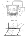
- the flow dispensing equipment 17 is shown diagrammatically in FIG. 2.
- the flow 18 (benzyl alpha 102-1500 or equivalent) is placed in a teflon tank 19, enclosed in a stainless steel cylinder 19a, the removable bottom of which constitutes the flux mask 20.
- This mask is pierced with holes 21 according to the configuration and the pitch of the pins.
- the pressure inside the reservoir 19 is controlled from a pneumatic system 22 controlled for example, from a logic circuit or from an analog output of a computer (not shown).
- the flow is maintained in the tank during the positioning phase, that is to say approaching and aligning the tank above the ceramic substrate 11, then is released by means of a pressure pulse supplied by the system. 22.
- the substrate 11 is placed in a substrate support 23 provided with alignment pins (not shown).
- a flux droplet 24 as can be seen in FIG. 3.
- the holes 21 must have a diameter of 0.4mm, while the thickness of the fabric constituting the flux mask is 1mm.
- the purpose of the second step is to define other equipment which can ensure the suction, the maintenance, and the release of a solder ball above each spindle head where it will be maintained by the adhesive action of the droplet of the flux deposited during the first step.
- the Pb / Sn 90/10 solder balls chosen for this application have a diameter of 0.7mm, they are also very light, we therefore planned to vibrate them, before sucking them up, that's the role of the equipment shown in Figures 4A.
- the balls 25 are agitated in a vibrating bowl 26 controlled by a vibrator 27.
- This vibrating bowl must be made with a sufficiently elastic material so that the solder balls can bounce on it.
- a vibrating bowl made of polyethylene was entirely satisfactory. Furthermore, the vibrations have been found to be insufficient in themselves to put the balls in agitation. It was shown that there was an optimum number of solder balls which actually corresponded to a monolayer of balls when the bowl was at rest.
- the vibrator 27 included a table resting on two oblique springs 27a, an electromagnet 27b ensuring the vibration of the assembly.
- the balls vibrated over a height of about 20mm.
- Other embodiments of stirring the balls can be envisaged, for example with a container whose bottom is porous and receives compressed air.
- FIG 4B there is shown an equipment 28 for suction and dispensing of solder balls, which sucks the moving balls in the vibrating bowl 26.
- This equipment comprises a soft iron frame 29 which can be circular in shape , and which defines a suction chamber 30 in connection, by a tube 31, with a controlled vacuum device (not shown).
- An electromagnet 32 is arranged along the tubing which constitutes its axis, it is controlled from the mains voltage (50 Hz) through a diode.
- the suction chamber is closed by a suction mask 33 provided with a rod 34, the other end of which is located in the air gap of the electromagnet.
- the mask consists of a 0.1mm thick beryllium copper membrane, pierced with holes according to the configuration of the pins on the substrate. The diameter of the suction holes is 0.4mm.
- the vibrator 27 is first set in motion to ensure the agitation of the balls 25 in the vibrating bowl 26.
- the equipment 28 previously connected at the source of vacuum, is immersed in the vibrating bowl so that the distance between the suction mask 33 and the bottom of the bowl is about 5mm.
- the time required to take all the balls is of the order of one second.
- the equipment 28 carrying the solder balls 25 is placed above the substrate 11 and arranged so that the configuration of balls and that of the pins are aligned with however preferably a slight offset so that the ball rests on at least one portion of the carnation.
- This alignment can be done thanks to the presence of alignment pins (not shown) on the module support, which receive corresponding recesses (not shown) made in the frame of the equipment 28 similar to that shown in the figure. 2.
- the solder balls are therefore brought into contact with the corresponding flux droplets.
- the vacuum is then cut; while the electromagnet is controlled for approximately 0.5 seconds. It has been noticed that the process was greatly improved by the vibration of the membrane. This has the effect of helping to loosen the balls which remain however maintained on the spindle heads thanks to the adhesive action of the flux.
- FIG. 5 represents the arrangement of the balls on the ceramic substrate.
- the existence of a slight difference between the spindle head 15a and the solder ball 25 is clearly highlighted in this figure. It has been noted that this offset provides better adhesion of the ball to the flow, and better welding between the spindle head and the eyelet. This results in better yields. It only remains, in a known manner, only to dispense flux (for example using equipment similar to that described in FIG. 2) on the fingers at the ends of the conductors at the location of the solder balls. of the silicon chip, and to place this chip.
- the ceramic substrate is finally introduced into a nitrogen atmosphere furnace having a temperature peak at 350 ° C., which melts the solder balls and which simultaneously ensures the bonding of the chip with the fingers of the conductors deposited on the substrate (technique said Flip-Chip) and the connection of the pin heads with the eyelets of said conductors.
Abstract
Ce procédé pour souder les têtes (15a) des broches de connexion (15) préalablement insérées dans un substrat céramique (11), aux oeillets (13) de la configuration de conducteurs formée sur la surface dudit substrat, comporte les étapes suivantes: - application d'une gouttelette de flux (24) sur chaque tête de broche (15a), - application d'une bille de soudure (25) sur chaque tête de broche où elle est maintenue en place par l'action adhésive de flux, - chauffage dans un four à azote présentant un pic de temperature à 350°C pour faire fondre la soudure et refroidissement pour figer la soudure et assurer une liaison permanente électrique et mécanique entre la tête de broche et l'oeillet. Application à la fabrication des modules électroniques utilises dans les calculateurs.This process for welding the heads (15a) of the connection pins (15) previously inserted in a ceramic substrate (11), to the eyelets (13) of the configuration of conductors formed on the surface of said substrate, comprises the following steps: - application a flux droplet (24) on each spindle head (15a), - application of a solder ball (25) on each spindle head where it is held in place by the adhesive flux action, - heating in a nitrogen furnace having a temperature peak at 350 ° C to melt the solder and cooling to freeze the solder and ensure a permanent electrical and mechanical connection between the spindle head and the eyelet. Application to the manufacture of electronic modules used in computers.
Description
La présente invention concerne le domaine de la fabrication des modules électroniques et plus particulièrement un procédé pour souder les têtes de broches aux oeillets de conducteurs, formés selon une configuration déterminée à la surface d'un substrat céramique.The present invention relates to the field of manufacturing electronic modules and more particularly to a method for soldering pin heads to conductor eyelets, formed according to a predetermined configuration on the surface of a ceramic substrate.
L'industrie des circuits intégrés à semi-conducteurs fait de plus en plus appel aux modules électroniques pour servir d'emballage aux microplaquettes de silicium. Ces modules électroniques, dans un mode de réalisation courant, comprennent essentiellement un substrat céramique revêtu d'une configuration déterminée de conducteurs métalliques qui relient les plots de soudure de la microplaquette aux broches (Flip-Chip technique). Ces dernières assurent les liaisons mécaniques et électriques avec le monde extérieur. L'ensemble est généralement protégé par un capot métallique ou plastique. Les conducteurs, aux emplacements des- broches, présentent des oeillets. Un problème important, qui se pose sur les lignes de fabrication de ces modules est d'assurer de bonnes liaisons électrique et mécanique entre la tête de la broche, généralement renflée, et la partie du conducteur en forme d'oeillet à cet endroit.The semiconductor integrated circuits industry is making increasing use of electronic modules to package silicon chips. These electronic modules, in a current embodiment, essentially comprise a ceramic substrate coated with a determined configuration of metallic conductors which connect the solder pads of the chip to the pins (Technical Flip-Chip). These provide mechanical and electrical connections to the outside world. The assembly is generally protected by a metal or plastic cover. The conductors, at the pin locations, have eyelets. An important problem which arises on the production lines of these modules is to ensure good electrical and mechanical connections between the head of the spindle, generally swollen, and the part of the conductor in the form of an eyelet at this location.
L'état de la technique comporte de très nombreux procédés qui ont été développés pour assurer la liaison électrique entre cet oeillet et la tête de broche.The state of the art comprises numerous methods which have been developed to provide the electrical connection between this eyelet and the spindle head.
Un premier procédé classique consiste à appliquer un anneau de soudure autour de la tête de broche, et de passer ensuite le module dans un four. Une description de ce procédé peut être trouvée dans un article intitulé: "Solder Ring Application Tool" par R.F. Buczak et al paru dans la publication de l'IBM Technical Disclosure Bulletin, Vol. 12, No.l, juin 1969, pages 15 et 16.A first conventional method consists in applying a solder ring around the spindle head, and then passing the module through an oven. A description of this process can be found in an article entitled: "Solder Ring Application Tool" by R.F. Buczak et al published in the publication of the IBM Technical Disclosure Bulletin, Vol. 12, No. 1, June 1969,
Ce procédé implique pratiquement l'utilisation de broches cylindriques (donc sans tête renflée), et présente alors des inconvénients lors de la manipulation du substrat muni de ses broches. En outre le moindre déplacement de l'anneau de soudure ou son mauvais placement peut causer une soudure incomplète ou même un court-circuit entre deux têtes de broches.This process practically involves the use of cylindrical pins (therefore without a bulging head), and therefore has drawbacks when handling the substrate provided with its pins. In addition, the slightest displacement of the solder ring or its improper placement can cause incomplete soldering or even a short circuit between two pin heads.
On a pensé également assurer cette soudure dans un bain électrolytique comme le suggère l'article: "Pin Bonding Technique" de F.C. Campagna et al, paru dans la publication de l'IBM Technical Disclosure Bulletin, Vol. 14, No.11, avril 1972, pages 3246 et 3247. Outre sa complexité, ce procédé est très contaminant, ce qui peut nuire à la fiabilité du module une fois encapsulé.We also thought to ensure this welding in an electrolytic bath as suggested in the article: "Pin Bonding Technique" by F.C. Campagna et al, published in the publication of the IBM Technical Disclosure Bulletin, Vol. 14, No. 11, April 1972, pages 3246 and 3247. In addition to its complexity, this process is very contaminating, which can harm the reliability of the module once encapsulated.
Les substrats peuvent être également étamés par la technique de trempage bien connue. Cette technique est très coûteuse en matières premières (flux, soudure, perchloréthylène) et en main d'oeuvré (étamage et tri visuel).The substrates can also be tinned by the well known dipping technique. This technique is very expensive in raw materials (flux, welding, perchlorethylene) and in labor (tinning and visual sorting).
Encore une autre technique classique, consiste à effectuer l'étamage au moyen d'une pâte de soudure dispensée au moment du placement de la microplaquette. Cette technique présente deux inconvénients majeurs: la dispense de la pâte sur les têtes de broche est une étape de réalisation difficile, et la présence fréquente de résidus de soudure est susceptible de causer des court-circuits entre les conducteurs.Yet another conventional technique consists in carrying out tinning using a solder paste dispensed at the time of placing the chip. This technique has two major drawbacks: dispensing the paste on the spindle heads is a difficult step in the production, and the frequent presence of solder residue is likely to cause short circuits between the conductors.
Une technique voisine est décrite dans un article intitulé "Solder Creme Dispensing Nozzle" par G. Sabol et J. Siwy publié dans l'IBM Technical Disclosure Bulletin, Vol. 14, No.7, december 1971, page 2090.A similar technique is described in an article entitled "Solder Creme Dispensing Nozzle" by G. Sabol and J. Siwy published in the IBM Technical Disclosure Bulletin, Vol. 14, No. 7, December 1971, page 2090.
Toutes ces techniques, impliquent la liaison des têtes de broches aux oeillets avant la liaison des microplaquettes munies de billes de soudure, aux doigts conducteurs portés par le substrat céramique. A cette occasion, de la soudure venait souvent se déposer sur ces doigts, ce qui rendait l'alignement de la microplaquette plus difficile. Une des solutions retenues consistait à effectuer une étape de brossage supplémentaire pour enlever ces dépôts non désirés de soudure.All these techniques involve the connection of the pin heads to the eyelets before the connection of the microchips provided with solder balls, to the conductive fingers carried by the ceramic substrate. On this occasion, welding was often deposited on these fingers, which made alignment of the chip more difficult. One of the solutions adopted consisted in carrying out an additional brushing step to remove these unwanted weld deposits.
Ces inconvénients sont évités avec le procédé de la présente invention ayant comme caractéristique principale celle de la partie caractérisante de la revendication 1, et qui dans son principe consiste à placer des billes de soudure sur les têtes de broches préalablement fluxées. La liaison entre les têtes de broche et les oeillets s'effectue dans un four, par la fusion des billes de soudure, par exemple simultanément avec la liaison de la microplaquette.These drawbacks are avoided with the method of the present invention having as main characteristic that of the characterizing part of claim 1, and which in principle consists in placing solder balls on the heads of the pins previously fluxed. The connection between the spindle heads and the eyelets takes place in an oven, by the fusion of the solder balls, for example simultaneously with the connection of the chip.
De façon plus détaillée le présent procédé comporte les étapes suivantes :
- application d'une gouttelette de flux sur chacune des têtes de broche,
- application d'une bille de soudure sur chacune desdites têtes de broche où elle est maintenue par l'action adhésive du flux,
- chauffage pour fondre les billes de soudure et assurer une liaison permanente entre les têtes de broches et les oeillets correspondants et refroidissement pour permettre à la soudure de se solidifier.
- application of a flux droplet on each of the spindle heads,
- application of a solder ball on each of said spindle heads where it is maintained by the adhesive action of the flux,
- heating to melt the solder balls and ensure a permanent connection between the pin heads and the corresponding eyelets and cooling to allow the solder to solidify.
L'application d'une bille de soudure sur chaque tête de broche a nécessité des équipements appropriés, dont la réalisation s'est révélée particulièrement difficile. Ces équipements sont décrits dans la partie caractérisante des revendications 3 à 8.The application of a solder ball on each spindle head required appropriate equipment, the production of which proved to be particularly difficult. This equipment is described in the characterizing part of claims 3 to 8.
Le présent procédé peut être facilement automatisé et démontre une fiabilité pratiquement parfaite.The present process can be easily automated and demonstrates practically perfect reliability.
L'invention est exposée ci-après, de façon détaillée à l'aide des dessins qui représentent seulement un mode de réalisation.The invention is set out below in detail using the drawings which represent only one embodiment.
- La figure 1 représente une vue partiellement éclatée d'une portion d'un module électronique classique dont le capot protecteur a été retiré, et laissant apparaître le substrat céramique métallisé.FIG. 1 represents a partially exploded view of a portion of a conventional electronic module from which the protective cover has been removed, and revealing the metallized ceramic substrate.
- La figure 2 représente l'équipement de fluxage destiné à assurer la dispense d'une goutte de- flux sur chaque tête de broche.FIG. 2 represents the fluxing equipment intended to ensure the dispensing of a drop of flux on each spindle head.
- La figure 3 représente schématiquement une vue en coupe du substrat céramique métallisé de la figure 1 selon la ligne I-I, après fluxage.Figure 3 schematically shows a sectional view of the metallized ceramic substrate of Figure 1 along line I-I, after fluxing.
- Les figures 4A et 4B représentent respectivement un équipement de mise en agitation des billes de soudure et un équipement d'aspiration et de dispense de ces billes.FIGS. 4A and 4B respectively represent an equipment for stirring the solder balls and a suction and dispensing equipment for these balls.
- La figure 5 représente schématiquement le substrat montré sur la figure 3 après l'étape de dispense des billes de soudure.FIG. 5 schematically represents the substrate shown in FIG. 3 after the step of dispensing the solder balls.
La figure 1 représente une vue partiellement éclatée d'une portion d'un module électronique 10 classique dont le capot protecteur a été retiré. Il comprend un substrat céramique 11 muni d'une configuration de conducteurs métalliques 12, qui présentent un élargissement en forme d'oeillet 13 à l'emplacement des trous 14 où sont insérées les broches de connexion 15.FIG. 1 represents a partially exploded view of a portion of a conventional
Il faut comprendre qu'il existe une infinité de configurations possibles ': pour l'implantation des broches (cependant elles sont généralement disposées selon une matrice avec un pas d'espacement déterminé) et pour la disposition de conducteurs métalliques.It should be understood that there are an infinity of possible configurations': for the implantation of the pins (however they are generally arranged according to a matrix with a no determined spacing) and for the arrangement of metallic conductors.
Chaque broche 15 présente un renflement 15a sur sa partie supérieure qui constitue la tête de la broche. Après insertion de la broche dans son trou, la tête de la broche 15a doit être soudée à l'oeillet 13, cette opération une fois achevée laisse un plot de soudure 16.Each
La présente invention se propose de fournir un procédé nouveau pour assurer cette opération, de soudage, qui assure la liaison mécanique et électrique de la tête de broche avec l'oeillet du conducteur correspondant.The present invention proposes to provide a new method for performing this welding operation, which ensures the mechanical and electrical connection of the spindle head with the eyelet of the corresponding conductor.
La première étape de ce procédé consiste dans la dispense d'une gouttelette de flux au-dessus de chaque tête de broche. L'équipement de dispense du flux 17 est représenté schématiquement sur la figure 2. Le flux 18 (benzylique alpha 102-1500 ou équivalent) est placé dans un réservoir en téflon 19, enfermé dans un cylindre en inox 19a, dont le fond amovible constitue le masque de fluxage 20. Ce masque est percé de trous 21 selon la configuration et le pas des broches. La pression à l'intérieur du réservoir 19 est contrôlée à partir d'un système pneumatique 22 commandé par exemple, à partir d'un circuit logique ou d'une sortie analogique d'un ordinateur (non représenté). Le flux est maintenu dans le réservoir pendant la phase de positionnement, c'est-à-dire d'approche et d'alignement du réservoir au-dessus du substrat céramique 11, puis est libéré grâce à une impulsion de pression fournie par le système 22. Le substrat 11 est disposé dans un support de substrat 23 muni de broches d'alignement (non représentées). Après que l'équipement ait été retiré, il reste au-dessus de chaque tête de broche, une gouttelette de flux 24 comme on peut s'en rendre compte sur la figure 3. Pour des têtes de broches de diamètre φ =0,7mm, il s'est révélé qu'un espacement masque-tête de 0,1mm était souhaitable. Dans ces conditions, les trous 21 doivent avoir un diamètre de 0,4mm, tandis que l'épaisseur de la toile constituant le masque de fluxage est de lmm.The first step in this process consists in dispensing a droplet of flux above each spindle head. The
La deuxième étape a pour objet de définir d'autres équipements qui puissent assurer l'aspiration, le maintien, et la libération d'une bille de soudure au-dessus de chaque tête de broche où elle sera maintenue par l'action adhésive de la gouttelette du flux déposé lors de la première étape.The purpose of the second step is to define other equipment which can ensure the suction, the maintenance, and the release of a solder ball above each spindle head where it will be maintained by the adhesive action of the droplet of the flux deposited during the first step.
Les billes de soudure Pb/Sn 90/10 choisies pour cette application, ont un diamètre de 0,7mm, elles sont par ailleurs très légères, on a donc prévu de les mettre en vibration, avant de les aspirer, c'est le rôle de l'équipement montré sur la figures 4A. Les billes 25 sont agitées dans un bol vibrant 26 commandé par un vibrateur 27. Ce bol vibrant doit être réalisé avec un matériau suffisamment élastique pour que les billes de soudure puissent rebondir dessus. Un bol vibrant réalisé en polyéthylène a donné entière satisfaction. Par ailleurs, les vibrations se sont révélées insuffisantes a elles seules pour mettre les billes en agitation. On a mis en évidence qu'il y avait un nombre optimum de billes de soudure qui correspondait en fait à une monocouche de billes quand le bol était au repos. Dans la réalisation préférée sus-mentionnée, .le bol était un parallèlépipède de base carrée (70mm x 70mm) et de hauteur H= 80mm. Le vibrateur 27 comprenait une table reposant sur deux ressorts obliques 27a, un électro-aimant 27b assurant la mise en vibration de l'ensemble.The Pb / Sn 90/10 solder balls chosen for this application, have a diameter of 0.7mm, they are also very light, we therefore planned to vibrate them, before sucking them up, that's the role of the equipment shown in Figures 4A. The
Dans ces conditions, les billes vibraient sur une hauteur d'environ 20mm. D'autres modes de réalisation de la mise en agitation des billes, peuvent être envisagés par exemple avec un récipient dont le fond est poreux et reçoit de l'air comprimé.Under these conditions, the balls vibrated over a height of about 20mm. Other embodiments of stirring the balls can be envisaged, for example with a container whose bottom is porous and receives compressed air.
Sur la figure 4B, on a représenté un équipment 28 d'aspiration et de dispense des billes de soudure, qui vient aspirer les billes en mouvement dans le bol vibrant 26. Cet équipement comprend un bâti en fer doux 29 qui peut être de forme circulaire, et qui définit une chambre d'aspiration 30 en liaison, par une tubulure 31, avec un dispositif à vide commandé (non représenté). Un électro-aimant 32 est disposé le long de la tubulure qui en constitue l'axe, il est commandé à partir de la tension du secteur (50 Hz) à travers une diode. La chambre d'aspiration est fermée par un masque d'aspiration 33 munie d'une tige 34 dont l'autre extrémité se trouve dans l'entrefer de l'électro-aimant. Le masque est constitué par une membrane de cuivre au béryllium de 0,1mm d'épaisseur, percé de trous selon la configuration des broches sur le substrat. Le diamètre des trous d'aspiration est de 0,4mm.In Figure 4B, there is shown an
Le fonctionnement global des équipements représentés sur les figures 4A et 4B peut être compris de la manière suivante : le vibrateur 27 est d'abord mis en mouvement pour assurer l'agitation des billes 25 dans le bol vibrant 26. L'équipement 28 préalablement relié à la source de vide, est plongé dans le bol vibrant de telle sorte que la distance entre le masque d'aspiration 33 et le fond du bol soit d'environ 5mm. Le temps nécessaire pour prendre toutes les billes est de l'ordre d'une seconde. L'équipement 28 portant les billes de soudure 25 est placé au-dessus du substrat 11 et disposé de telle sorte que la configuration de billes et celle des broches soient alignées avec cependant de préférence un léger décalage pour que la bille repose sur au moins une portion de l'oeillet. Cet alignement peut se faire grâce à la présence de broches d'alignement (non représentées) sur le support de module, qui reçoivent des évidements .(non représentés) correspondants pratiqués dans le bâti de l'équipement 28 similaire à celui représenté sur la figure 2. Les billes de soudure sont donc amenées en contact avec les gouttelettes de flux correspondantes. Le vide est alors coupé; tandis que l'électro-aimant est commandé pendant environ 0,5 seconde. On a effet remarqué que le procédé était grandement amélioré par la mise en vibration de la membrane. Celà.pour effet d'aider à relâcher les billes qui restent cependant maintenues sur les têtes de broche grâce à l'action adhésive du flux.The overall operation of the equipment shown in Figures 4A and 4B can be understood as follows: the
La figure 5 représente la disposition des billes sur le substrat céramique. L'existence d'un léger décalage entre la tête de broche 15a et la bille de soudure 25 est clairement mise en évidence sur cette figure. On a remarqué que ce décalage procurait une meilleure adhésion de la bille au flux, et une meilleure soudure entre la tête de broche et l'oeillet. Il en résulte de meilleurs rendements. Il ne reste plus, de manière connue, qu'à dispenser du flux (par exemple à l'aide d'un équipement similaire à celui décrit sur la figure 2) sur les doigts aux extrémités des conducteurs à l'emplacement des billes de soudure de la microplaquette de silicium, et à poser cette microplaquette. Le substrat céramique est enfin introduit dans un four à atmosphère d'azote présentant un pic de température à 350°C, qui fond les billes de soudure et qui assure simultanément la liaison de la microplaquette avec les doigts des conducteurs déposés sur le substrat (technique dite Flip-Chip) et la liaison des têtes de broches avec les oeillets desdits conducteurs.FIG. 5 represents the arrangement of the balls on the ceramic substrate. The existence of a slight difference between the spindle head 15a and the
Claims (10)
Priority Applications (4)
| Application Number | Priority Date | Filing Date | Title |
|---|---|---|---|
| EP81430045A EP0082902B1 (en) | 1981-12-29 | 1981-12-29 | Soldering method of pins to eyelets of conductors formed on a ceramic substrate |
| DE8181430045T DE3173078D1 (en) | 1981-12-29 | 1981-12-29 | Soldering method of pins to eyelets of conductors formed on a ceramic substrate |
| JP57162407A JPS58118131A (en) | 1981-12-29 | 1982-09-20 | Bonding method |
| US06/452,530 US4462534A (en) | 1981-12-29 | 1982-12-23 | Method of bonding connecting pins to the eyelets of conductors formed on a ceramic substrate |
Applications Claiming Priority (1)
| Application Number | Priority Date | Filing Date | Title |
|---|---|---|---|
| EP81430045A EP0082902B1 (en) | 1981-12-29 | 1981-12-29 | Soldering method of pins to eyelets of conductors formed on a ceramic substrate |
Publications (2)
| Publication Number | Publication Date |
|---|---|
| EP0082902A1 true EP0082902A1 (en) | 1983-07-06 |
| EP0082902B1 EP0082902B1 (en) | 1985-11-27 |
Family
ID=8188606
Family Applications (1)
| Application Number | Title | Priority Date | Filing Date |
|---|---|---|---|
| EP81430045A Expired EP0082902B1 (en) | 1981-12-29 | 1981-12-29 | Soldering method of pins to eyelets of conductors formed on a ceramic substrate |
Country Status (4)
| Country | Link |
|---|---|
| US (1) | US4462534A (en) |
| EP (1) | EP0082902B1 (en) |
| JP (1) | JPS58118131A (en) |
| DE (1) | DE3173078D1 (en) |
Cited By (9)
| Publication number | Priority date | Publication date | Assignee | Title |
|---|---|---|---|---|
| FR2602920A1 (en) * | 1986-04-24 | 1988-02-19 | Souriau & Cie | Connector having an integrated attenuation filter |
| EP0263222A1 (en) * | 1986-10-08 | 1988-04-13 | International Business Machines Corporation | Method of forming solder terminals for a pinless ceramic module |
| EP0263221A1 (en) * | 1986-10-08 | 1988-04-13 | International Business Machines Corporation | Method of forming solder bumps on metal contact pads of a substrate |
| EP0447170A2 (en) * | 1990-03-14 | 1991-09-18 | Nippon Steel Corporation | Method of bonding bumps to leads of tab tape and an apparatus for arranging bumps used for the same |
| EP0463559A2 (en) * | 1990-06-25 | 1992-01-02 | Fujitsu Limited | Packaged semiconductor device and a manufacturing process therefor |
| EP0582375A1 (en) * | 1992-08-04 | 1994-02-09 | International Business Machines Corporation | Solder particle deposition |
| US5293072A (en) * | 1990-06-25 | 1994-03-08 | Fujitsu Limited | Semiconductor device having spherical terminals attached to the lead frame embedded within the package body |
| EP1617519A2 (en) * | 1996-10-10 | 2006-01-18 | Fci | High density connector |
| CH698875B1 (en) * | 2007-07-25 | 2009-11-30 | Sauter Ag | Printed circuit board assembling method for switching device of room apparatus, involves resting head of pin at edge of bore when pin is completely arranged through bore, and soldering head of pin on carrier over solder area |
Families Citing this family (63)
| Publication number | Priority date | Publication date | Assignee | Title |
|---|---|---|---|---|
| US4558812A (en) * | 1984-11-07 | 1985-12-17 | At&T Technologies, Inc. | Method and apparatus for batch solder bumping of chip carriers |
| US5917707A (en) | 1993-11-16 | 1999-06-29 | Formfactor, Inc. | Flexible contact structure with an electrically conductive shell |
| US4761699A (en) * | 1986-10-28 | 1988-08-02 | International Business Machines Corporation | Slider-suspension assembly and method for attaching a slider to a suspension in a data recording disk file |
| JPH0795554B2 (en) * | 1987-09-14 | 1995-10-11 | 株式会社日立製作所 | Solder ball alignment device |
| US5088639A (en) * | 1991-01-25 | 1992-02-18 | Motorola, Inc. | Soldering process |
| US5145104A (en) * | 1991-03-21 | 1992-09-08 | International Business Machines Corporation | Substrate soldering in a reducing atmosphere |
| US5205896A (en) * | 1992-02-03 | 1993-04-27 | Hughes Aircraft Company | Component and solder preform placement device and method of placement |
| US5788143A (en) * | 1992-04-08 | 1998-08-04 | International Business Machines Corporation | Solder particle deposition |
| US5284287A (en) * | 1992-08-31 | 1994-02-08 | Motorola, Inc. | Method for attaching conductive balls to a substrate |
| JPH0828583B2 (en) * | 1992-12-23 | 1996-03-21 | インターナショナル・ビジネス・マシーンズ・コーポレイション | Multilayer printed circuit board, manufacturing method thereof, and ball dispenser |
| US5323947A (en) * | 1993-05-03 | 1994-06-28 | Motorola, Inc. | Method and apparatus for use in forming pre-positioned solder bumps on a pad arrangement |
| US5416872A (en) * | 1993-07-06 | 1995-05-16 | At&T Corp. | Arrangement for interconnecting an optical fiber an optoelectronic component |
| US5345529A (en) * | 1993-07-06 | 1994-09-06 | At&T Bell Laboratories | Method for assembly of an optical fiber connective device |
| US5820014A (en) | 1993-11-16 | 1998-10-13 | Form Factor, Inc. | Solder preforms |
| US20020053734A1 (en) | 1993-11-16 | 2002-05-09 | Formfactor, Inc. | Probe card assembly and kit, and methods of making same |
| US5431332A (en) * | 1994-02-07 | 1995-07-11 | Motorola, Inc. | Method and apparatus for solder sphere placement using an air knife |
| JP3528264B2 (en) * | 1994-08-19 | 2004-05-17 | ソニー株式会社 | Solder ball mounting device |
| US5650595A (en) * | 1995-05-25 | 1997-07-22 | International Business Machines Corporation | Electronic module with multiple solder dams in soldermask window |
| TW267265B (en) * | 1995-06-12 | 1996-01-01 | Connector Systems Tech Nv | Low cross talk and impedance controlled electrical connector |
| US6939173B1 (en) * | 1995-06-12 | 2005-09-06 | Fci Americas Technology, Inc. | Low cross talk and impedance controlled electrical connector with solder masses |
| US5685477A (en) * | 1995-06-28 | 1997-11-11 | Intel Corporation | Method for attaching and handling conductive spheres to a substrate |
| US5899376A (en) * | 1995-07-11 | 1999-05-04 | Nippon Steel Corporation | Transfer of flux onto electrodes and production of bumps on electrodes |
| JP3120714B2 (en) * | 1995-10-31 | 2000-12-25 | 松下電器産業株式会社 | Mounting device for conductive balls |
| US5687901A (en) * | 1995-11-14 | 1997-11-18 | Nippon Steel Corporation | Process and apparatus for forming ball bumps |
| US8033838B2 (en) | 1996-02-21 | 2011-10-11 | Formfactor, Inc. | Microelectronic contact structure |
| US5994152A (en) | 1996-02-21 | 1999-11-30 | Formfactor, Inc. | Fabricating interconnects and tips using sacrificial substrates |
| US6024584A (en) * | 1996-10-10 | 2000-02-15 | Berg Technology, Inc. | High density connector |
| US6093035A (en) * | 1996-06-28 | 2000-07-25 | Berg Technology, Inc. | Contact for use in an electrical connector |
| US6241535B1 (en) | 1996-10-10 | 2001-06-05 | Berg Technology, Inc. | Low profile connector |
| US6042389A (en) * | 1996-10-10 | 2000-03-28 | Berg Technology, Inc. | Low profile connector |
| SG71046A1 (en) | 1996-10-10 | 2000-03-21 | Connector Systems Tech Nv | High density connector and method of manufacture |
| US6139336A (en) | 1996-11-14 | 2000-10-31 | Berg Technology, Inc. | High density connector having a ball type of contact surface |
| US6441487B2 (en) | 1997-10-20 | 2002-08-27 | Flip Chip Technologies, L.L.C. | Chip scale package using large ductile solder balls |
| US6272741B1 (en) * | 1998-07-24 | 2001-08-14 | Autosplice, Inc. | Hybrid solder ball and pin grid array circuit board interconnect system and method |
| US6193143B1 (en) * | 1998-08-05 | 2001-02-27 | Matsushita Electric Industrial Co., Ltd. | Solder bump forming method and mounting apparatus and mounting method of solder ball |
| US6595408B1 (en) * | 1998-10-07 | 2003-07-22 | Micron Technology, Inc. | Method of attaching solder balls to BGA package utilizing a tool to pick and dip the solder ball in flux prior to placement |
| US6268275B1 (en) | 1998-10-08 | 2001-07-31 | Micron Technology, Inc. | Method of locating conductive spheres utilizing screen and hopper of solder balls |
| US6711812B1 (en) | 1999-04-13 | 2004-03-30 | Unicap Electronics Industrial Corporation | Method of making metal core substrate printed circuit wiring board enabling thermally enhanced ball grid array (BGA) packages |
| US6675472B1 (en) | 1999-04-29 | 2004-01-13 | Unicap Electronics Industrial Corporation | Process and structure for manufacturing plastic chip carrier |
| US6589594B1 (en) * | 2000-08-31 | 2003-07-08 | Micron Technology, Inc. | Method for filling a wafer through-via with a conductive material |
| US6928727B2 (en) * | 2002-07-30 | 2005-08-16 | Avx Corporation | Apparatus and method for making electrical connectors |
| US6860741B2 (en) | 2002-07-30 | 2005-03-01 | Avx Corporation | Apparatus and methods for retaining and placing electrical components |
| US6851954B2 (en) | 2002-07-30 | 2005-02-08 | Avx Corporation | Electrical connectors and electrical components |
| WO2005011060A2 (en) * | 2003-07-16 | 2005-02-03 | Gryphics, Inc. | Electrical interconnect assembly with interlocking contact system |
| US7537461B2 (en) * | 2003-07-16 | 2009-05-26 | Gryphics, Inc. | Fine pitch electrical interconnect assembly |
| US7297003B2 (en) * | 2003-07-16 | 2007-11-20 | Gryphics, Inc. | Fine pitch electrical interconnect assembly |
| JP4370225B2 (en) * | 2004-08-19 | 2009-11-25 | 住友電装株式会社 | Terminal mounting method on printed circuit board, terminal mounting printed circuit board formed by the method, and electrical junction box containing the terminal mounting printed circuit board |
| US7684205B2 (en) * | 2006-02-22 | 2010-03-23 | General Dynamics Advanced Information Systems, Inc. | System and method of using a compliant lead interposer |
| JP4956609B2 (en) | 2006-03-20 | 2012-06-20 | グリフィクス インコーポレーティッド | Composite terminals for fine pitch electrical connection assemblies |
| US8366485B2 (en) | 2009-03-19 | 2013-02-05 | Fci Americas Technology Llc | Electrical connector having ribbed ground plate |
| CN102456958A (en) * | 2010-10-23 | 2012-05-16 | 富士康(昆山)电脑接插件有限公司 | Electrical connector and manufacturing method thereof |
| EP2624034A1 (en) | 2012-01-31 | 2013-08-07 | Fci | Dismountable optical coupling device |
| US9257778B2 (en) | 2012-04-13 | 2016-02-09 | Fci Americas Technology | High speed electrical connector |
| USD727268S1 (en) | 2012-04-13 | 2015-04-21 | Fci Americas Technology Llc | Vertical electrical connector |
| US8944831B2 (en) | 2012-04-13 | 2015-02-03 | Fci Americas Technology Llc | Electrical connector having ribbed ground plate with engagement members |
| USD718253S1 (en) | 2012-04-13 | 2014-11-25 | Fci Americas Technology Llc | Electrical cable connector |
| USD727852S1 (en) | 2012-04-13 | 2015-04-28 | Fci Americas Technology Llc | Ground shield for a right angle electrical connector |
| US9543703B2 (en) | 2012-07-11 | 2017-01-10 | Fci Americas Technology Llc | Electrical connector with reduced stack height |
| USD751507S1 (en) | 2012-07-11 | 2016-03-15 | Fci Americas Technology Llc | Electrical connector |
| USD745852S1 (en) | 2013-01-25 | 2015-12-22 | Fci Americas Technology Llc | Electrical connector |
| USD720698S1 (en) | 2013-03-15 | 2015-01-06 | Fci Americas Technology Llc | Electrical cable connector |
| US9138821B2 (en) * | 2014-01-17 | 2015-09-22 | Medtronic, Inc. | Methods for simultaneously brazing a ferrule and lead pins |
| US10727168B2 (en) * | 2014-09-15 | 2020-07-28 | Nxp B.V. | Inter-connection of a lead frame with a passive component intermediate structure |
Citations (2)
| Publication number | Priority date | Publication date | Assignee | Title |
|---|---|---|---|---|
| US3921285A (en) * | 1974-07-15 | 1975-11-25 | Ibm | Method for joining microminiature components to a carrying structure |
| US4206542A (en) * | 1978-03-13 | 1980-06-10 | General Dynamics Pomona Division | Solder preform loading method and apparatus |
Family Cites Families (6)
| Publication number | Priority date | Publication date | Assignee | Title |
|---|---|---|---|---|
| US3292240A (en) * | 1963-08-08 | 1966-12-20 | Ibm | Method of fabricating microminiature functional components |
| US3719981A (en) * | 1971-11-24 | 1973-03-13 | Rca Corp | Method of joining solder balls to solder bumps |
| SU651914A1 (en) * | 1977-03-24 | 1979-03-15 | Предприятие П/Я Г-4097 | Apparatus for making printed circuit boards |
| US4332341A (en) * | 1979-12-26 | 1982-06-01 | Bell Telephone Laboratories, Incorporated | Fabrication of circuit packages using solid phase solder bonding |
| US4396140A (en) * | 1981-01-27 | 1983-08-02 | Bell Telephone Laboratories, Incorporated | Method of bonding electronic components |
| US4421266A (en) * | 1981-07-29 | 1983-12-20 | Western Electric Company, Inc. | Handling bodies containing bonding material |
-
1981
- 1981-12-29 DE DE8181430045T patent/DE3173078D1/en not_active Expired
- 1981-12-29 EP EP81430045A patent/EP0082902B1/en not_active Expired
-
1982
- 1982-09-20 JP JP57162407A patent/JPS58118131A/en active Granted
- 1982-12-23 US US06/452,530 patent/US4462534A/en not_active Expired - Lifetime
Patent Citations (2)
| Publication number | Priority date | Publication date | Assignee | Title |
|---|---|---|---|---|
| US3921285A (en) * | 1974-07-15 | 1975-11-25 | Ibm | Method for joining microminiature components to a carrying structure |
| US4206542A (en) * | 1978-03-13 | 1980-06-10 | General Dynamics Pomona Division | Solder preform loading method and apparatus |
Non-Patent Citations (4)
| Title |
|---|
| IBM TECHNICAL DISCLOSURE BULLETIN, vol.12, no.1, juin 1969, New York (US) * |
| IBM TECHNICAL DISCLOSURE BULLETIN, vol.14, no.7, décembre 1971, New York (US) * |
| IBM TECHNICAL DISCLOSURE BULLETIN, vol.20, no.2, juillet 1977, New York (US) * |
| TECHNICAL DIGEST, no.55, juillet 1979, New York (US) * |
Cited By (14)
| Publication number | Priority date | Publication date | Assignee | Title |
|---|---|---|---|---|
| FR2602920A1 (en) * | 1986-04-24 | 1988-02-19 | Souriau & Cie | Connector having an integrated attenuation filter |
| EP0263222A1 (en) * | 1986-10-08 | 1988-04-13 | International Business Machines Corporation | Method of forming solder terminals for a pinless ceramic module |
| EP0263221A1 (en) * | 1986-10-08 | 1988-04-13 | International Business Machines Corporation | Method of forming solder bumps on metal contact pads of a substrate |
| EP0447170A3 (en) * | 1990-03-14 | 1992-03-25 | Nippon Steel Corporation | Method of bonding bumps to leads of tab tape and an apparatus for arranging bumps used for the same |
| EP0447170A2 (en) * | 1990-03-14 | 1991-09-18 | Nippon Steel Corporation | Method of bonding bumps to leads of tab tape and an apparatus for arranging bumps used for the same |
| EP0463559A2 (en) * | 1990-06-25 | 1992-01-02 | Fujitsu Limited | Packaged semiconductor device and a manufacturing process therefor |
| EP0463559A3 (en) * | 1990-06-25 | 1992-03-25 | Fujitsu Limited | Packaged semiconductor device and a manufacturing process therefor |
| US5293072A (en) * | 1990-06-25 | 1994-03-08 | Fujitsu Limited | Semiconductor device having spherical terminals attached to the lead frame embedded within the package body |
| US5403776A (en) * | 1990-06-25 | 1995-04-04 | Fujitsu Limited | Process of using a jig to align and mount terminal conductors to a semiconductor plastic package |
| EP0582375A1 (en) * | 1992-08-04 | 1994-02-09 | International Business Machines Corporation | Solder particle deposition |
| US5445313A (en) * | 1992-08-04 | 1995-08-29 | International Business Machines Corporation | Solder particle deposition |
| EP1617519A2 (en) * | 1996-10-10 | 2006-01-18 | Fci | High density connector |
| EP1617519A3 (en) * | 1996-10-10 | 2007-12-12 | Fci | High density connector |
| CH698875B1 (en) * | 2007-07-25 | 2009-11-30 | Sauter Ag | Printed circuit board assembling method for switching device of room apparatus, involves resting head of pin at edge of bore when pin is completely arranged through bore, and soldering head of pin on carrier over solder area |
Also Published As
| Publication number | Publication date |
|---|---|
| EP0082902B1 (en) | 1985-11-27 |
| JPS64819B2 (en) | 1989-01-09 |
| DE3173078D1 (en) | 1986-01-09 |
| JPS58118131A (en) | 1983-07-14 |
| US4462534A (en) | 1984-07-31 |
Similar Documents
| Publication | Publication Date | Title |
|---|---|---|
| EP0082902B1 (en) | Soldering method of pins to eyelets of conductors formed on a ceramic substrate | |
| US5447886A (en) | Method for mounting semiconductor chip on circuit board | |
| EP0352183B1 (en) | Process for mounting electronic micro components on a support, and intermediate product | |
| EP1449810B1 (en) | Method for manufacturing micro-electro-mechanical system using solder balls | |
| JP2001144126A (en) | Semiconductor device and manufacturing method | |
| FR2742687A1 (en) | SOLDER SUPPLY METHOD, SOLDER SUPPLY APPARATUS, AND WELDING METHOD | |
| JPH0771743B2 (en) | Apparatus and method for injection molding molten solder | |
| JP4220580B2 (en) | Semiconductor device manufacturing equipment | |
| FR2759616A1 (en) | AUTOMATED STACKING AND BRAZING APPARATUS FOR THREE-DIMENSIONAL STACKED MODULE DEVICES AND MANUFACTURING METHOD THEREOF | |
| US6722557B2 (en) | Flux cleaning method and method of manufacturing semiconductor device | |
| US20040245896A1 (en) | Piezoelectric device and manufacturing method therefor | |
| US6761302B1 (en) | Device mounting method | |
| FR2792861A1 (en) | METHOD FOR PRODUCING WELDING PLOTS ON A SUBSTRATE AND GUIDE FOR IMPLEMENTING THE METHOD | |
| WO2000077729A1 (en) | Device and method for making devices comprising at least a chip fixed on a support | |
| KR20190060287A (en) | Method of trasferring micro-device array | |
| FR2479639A1 (en) | Electronic component mounting process for PCB - uses metal bridges in contact with metal tracks to permit substrate flexing without damage to solder joints | |
| EP0793269B1 (en) | Semiconductor device having a chip with via hole soldered on a support, and its method of fabrication | |
| JP4505783B2 (en) | Solder bump manufacturing method and manufacturing apparatus | |
| EP0040669A1 (en) | Method of eliminating solder pads remaining on a ceramic substrate after removing a semiconductor chip by absorption in a porous copper block, and use in reworking modules | |
| JPH01209736A (en) | Method of replacing semiconductor element | |
| JP2001135660A (en) | Method and apparatus for ball transfer | |
| EP0242667B1 (en) | Soldering tool for electronic devices | |
| JPH05347474A (en) | Piece for temporarily fixing electronic part | |
| JPH11297729A (en) | Semiconductor package and forming method thereof | |
| JPH11214569A (en) | Method and device for forming bump |
Legal Events
| Date | Code | Title | Description |
|---|---|---|---|
| PUAI | Public reference made under article 153(3) epc to a published international application that has entered the european phase |
Free format text: ORIGINAL CODE: 0009012 |
|
| AK | Designated contracting states |
Designated state(s): DE FR GB |
|
| 17P | Request for examination filed |
Effective date: 19831021 |
|
| GRAA | (expected) grant |
Free format text: ORIGINAL CODE: 0009210 |
|
| AK | Designated contracting states |
Designated state(s): DE FR GB |
|
| REF | Corresponds to: |
Ref document number: 3173078 Country of ref document: DE Date of ref document: 19860109 |
|
| PLBE | No opposition filed within time limit |
Free format text: ORIGINAL CODE: 0009261 |
|
| STAA | Information on the status of an ep patent application or granted ep patent |
Free format text: STATUS: NO OPPOSITION FILED WITHIN TIME LIMIT |
|
| 26N | No opposition filed | ||
| PGFP | Annual fee paid to national office [announced via postgrant information from national office to epo] |
Ref country code: DE Payment date: 19951229 Year of fee payment: 15 |
|
| PGFP | Annual fee paid to national office [announced via postgrant information from national office to epo] |
Ref country code: GB Payment date: 19961126 Year of fee payment: 16 |
|
| PGFP | Annual fee paid to national office [announced via postgrant information from national office to epo] |
Ref country code: FR Payment date: 19961211 Year of fee payment: 16 |
|
| PG25 | Lapsed in a contracting state [announced via postgrant information from national office to epo] |
Ref country code: DE Effective date: 19970902 |
|
| PG25 | Lapsed in a contracting state [announced via postgrant information from national office to epo] |
Ref country code: GB Free format text: LAPSE BECAUSE OF NON-PAYMENT OF DUE FEES Effective date: 19971229 |
|
| PG25 | Lapsed in a contracting state [announced via postgrant information from national office to epo] |
Ref country code: FR Free format text: THE PATENT HAS BEEN ANNULLED BY A DECISION OF A NATIONAL AUTHORITY Effective date: 19971231 |
|
| GBPC | Gb: european patent ceased through non-payment of renewal fee |
Effective date: 19971229 |
|
| REG | Reference to a national code |
Ref country code: FR Ref legal event code: ST |