EP0080902B1 - Semiconductor memory device - Google Patents
Semiconductor memory device Download PDFInfo
- Publication number
- EP0080902B1 EP0080902B1 EP82306384A EP82306384A EP0080902B1 EP 0080902 B1 EP0080902 B1 EP 0080902B1 EP 82306384 A EP82306384 A EP 82306384A EP 82306384 A EP82306384 A EP 82306384A EP 0080902 B1 EP0080902 B1 EP 0080902B1
- Authority
- EP
- European Patent Office
- Prior art keywords
- signal
- buffer
- row
- column address
- memory device
- Prior art date
- Legal status (The legal status is an assumption and is not a legal conclusion. Google has not performed a legal analysis and makes no representation as to the accuracy of the status listed.)
- Expired
Links
Images


Classifications
-
- G—PHYSICS
- G11—INFORMATION STORAGE
- G11C—STATIC STORES
- G11C8/00—Arrangements for selecting an address in a digital store
- G11C8/18—Address timing or clocking circuits; Address control signal generation or management, e.g. for row address strobe [RAS] or column address strobe [CAS] signals
Definitions
- the present invention relates to a semiconductor memory device, more particularly to a circuit for controlling a column part of the semiconductor memory device.
- a write operation or a read operation is accomplished by first selecting the desired row line, that is, word line, and then selecting the desired column line, that is, bit line. This allows the selection of the memory cell located at the crossing point of the selected row and column lines and enables a write or read operation to be performed on that memory cell.
- a so-called address multiplex access method has been proposed, for example in United States of America Patent Specification No 3 969 706.
- a row address strobe signal is externally supplied to the memory to establish a row access mode.
- a column address strobe signal is externally supplied to establish a column access mode.
- the column access mode starts when the column address strobe signal and a column address enable signal are both given.
- the column address enable signal is usually generated after certain processing is completed, which processing is started by receiving the row address strobe signal.
- the recent trend in semiconductor memory devices is toward very high speed read and write access operations. That is, the write or read access time must be as short as possible.
- the prior art there is a disadvantage in that the above-mentioned memory access operation cannot be conducted at a very high speed. This is because it takes a relatively long time to produce the aforementioned column address enable signal by the processing step initiated by the row address strobe signal.
- a semiconductor memory device comprising a row address buffer for receiving a row address signal when a row address strobe signal is externally supplied to the semiconductor memory device; a column address buffer for receiving a column address signal when a column address strobe signal is externally supplied to the semiconductor memory device; a row decoder and a column decoder cooperating with the row and column address buffers, respectively, and selecting the desired one of the memory cells specified by the row and column address signals; an RAS part clock generator producing a first timing control signal when the row address strobe signal is supplied, the first timing control signal being used for enabling the row part of the device; and, a CAS part clock generator producing a timing control signal for enabling the column decoder in the presence of both the column address strobe signal and the first timing control signal, is characterised by a circuit which detects and holds the row address strobe CAS signal and which enables the column address buffer, the circuit comprising a first buffer control circuit and a second buffer control circuit, the first buffer control circuit
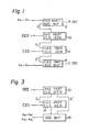
- FIG. 1 is a block diagram representing members for achieving memory cell selection in a prior art semiconductor memory device.
- the memory device of the present invention is based on the circuit arrangement shown in Fig. 1.
- reference symbol RAS indicates the aforementioned row address strobe signal.
- the signal RAS is received by a RAS part clock generator (RAS PART CLK GEN) 10 which produces clocks used for carrying out various controls in the RAS part, such as an address fetch, a precharge of a row decoder, and a row line selection.
- RAS part clock generator RAS part clock generator 10 which produces clocks used for carrying out various controls in the RAS part, such as an address fetch, a precharge of a row decoder, and a row line selection.
- Reference numeral 12 represents a RAS part address buffer i.e., row address buffer, (RAS PART ADD BUF), which is triggered by a signal S' and brings the external row address A o to A4 thereinto. Thereafter, the buffer 12 supplies an address, which is an inverted row address of A o to A4, to the row decoder (RDEC) (not shown in Fig. 1).
- Reference symbol CAS indicates the aforesaid column address strobe signal.
- the signal CAS is received by a CAS part clock generator (CAS PART CLK GEN) 14 which produces clocks used for carrying out various controls in the CAS part, such as identical to those mentioned above regarding the RAS part.
- Reference numeral 16 represents a CAS part address buffer (CAS PART ADD BUF), i.e., column address buffer, which is triggered by a timing control signal S" and brings the external column address A 5 to Ag thereinto. Thereafter, the buffer 14 supplies a column address to a column decoder (CDEC) (not shown in Fig. 1). It should be noted that the row address A o to A4 and the column address As to Ag are applied to the same address input pins of the memory device, but alternatively.
- CDEC column decoder
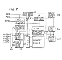
- Figure 2 is a block diagram representing a whole view of one example of a prior art semiconductor memory device employing the arrangement shown in Fig. 1.
- members the same as in Fig. 1 are represented by the same reference numerals or symbols.
- the block diagram of Fig. 2 may assist the understanding of the location of each member shown in Fig. 1 inside the semiconductor memory device.
- Figure 3 is a block diagram representing members, as in Fig. 1, for achieving another type of memory cell selection in a prior art semiconductor memory device. It is known that the arrangement of Fig. 3 is employed in a currently used Mostek type semiconductor memory device by Mostek Corporation of the U.S.A. In the arragement of Fig. 3, the RAS part address buffer 12 and the CAS part address buffer 16, both shown in Figs. 1 and 2, are commonly realized by a single address buffer (ADD BUF) 18. Since the row and column address buffers are realized by one buffer 18, the arrangement of Fig. 3 is advantageous from the viewpoint of pattern density in an integrated circuit (IC). However, the semiconductor memory device of the present invention is not based on such a common buffer type arrangement as in Fig. 3. In Fig. 3 and also Figs. 1 and 2, actually, inverted RAS and CAS signals are used. Therefore symbols RAS and CAS are used for the externally supplied row and column strobe signals, respectively.
- ADD BUF single address buffer
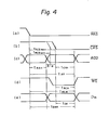
- Figure 4 is a timing diagram used for explaining the operations performed in Figs. 1 and 2.
- the RAS signal is supplied first (see row (a)).
- the row address fetch operation becomes enable.
- Reference symbol t RAH see row (c)) represents a term in which the row address is held. Therefore, the term t RAH may be called a row address hold (RAH) term.
- RAH row address hold
- t RCD' the level of the CAS signa! is changed to L (see row (b)
- the term t RCD denotes a time delay from the row access to the column access.
- Reference symbol t CAH (see row (c)) represents a term in which the column address fetch operation is carried out. Therefore, the term t CAH may be called a column address hold (CAH) term.
- CAH column address hold
- Reference symbol WE denotes a write enable signal. Actually, an inverted signal of WE, that is, WE, is used as shown at the top right in Fig. 2.
- WE an inverted signal of WE
- the read operation cycle is maintained. If the level of WE is changed from H to L (see row (d)), this means that a write operation cycle is specified.
- the specifying of the write operation cycle commences after completion of the row address fetch operation and also immediately after the level change of CAS from H to L.
- the write operation cycle is completed after the elapse of a write command hold (WCH) term t WCH (see row (d)).
- WCH write command hold
- the write operation is completed after the minimum term of t WCR (see row (e)), that is, t WCR min' and the minimum term of t WCH , that is, t WCH min' both elapse.
- t WCR min denotes the term from when the level of RAS changes to L to when the specifying of the write operation cycle is released.
- t WCH min denotes the term from when the level of CAS changes to L to when the specifying of the write operation cycle is released.
- Reference symbol D IN denotes a write data, as shown at the center right of Fig. 2.
- the level change of D IN is shown in row (e) of Fig. 4.
- reference symbol t DH denotes the term for holding the input write data D, N .
- the term t DHR is equal to the sum of t RCD max and t DH.
- the term t AR is equal to the sum of tRCD and tcAH.
- the trailing edge of the RAS signal and the trailing edge of the CAS signal must be shifted in time with each other so as to avoid row and column address fetch operation error. That is, first, the term t RAH is given for sufficiently holding the row address (A o -A4). After the elapse of the term T RAH , the row address (A o ⁇ A 4 ) is switched in an address bus AB (see bottom left in Fig. 2) to the column address (A5 ⁇ A9). If the switching term from the row address to the column address is represented by symbol 6 (see row (c) in Fig. 4), the trailing edge of the CAS signal must occur later than the trailing edge of the RAS signal, where the equation of must also stand.
- the term t RAH is given for sufficiently holding the row address (A o -A4).
- T RAH the row address (A o ⁇ A 4 ) is switched in an address bus AB (see bottom left in Fig. 2) to the column address (A5 ⁇ A9). If
- Figure 5 is a graph represeting the relationship between the terms t AR and t RCD' both shown in Fig. 4.
- the relationship between t AR and T RCD in the prior art semiconductor memory device is schematically represented by the characteristic curve shown by bent solid lines C, and C' 1 . It should be understood that each value of time is recited merely as an example.
- the term t AR is proportional to the term t RCD when the term t RCD is relatively long (refer to line C 1 ).
- t RCD when the term t RCD is shorter than a predetermined value of t RCD max (about 50 ns), the value of t AR is maintained at a fixed value (70 ns) defined by the predetermined value (50 ns) of t RCD mox and, thus, the value of t AR can no longer be shorter than the fixed value (refer to line C l ).
- the CAS part clock generator 14 is not driven until an AND logic between S, and CAS is satisfied, in which the signal S, is the aforesaid column address enable signal produced from the RAS part clock generator 10.
- the CAS part clock generator 14 starts operating when both the signal S 1 and CAS are applied thereto.
- the column address enable signal S is, in Fig. 5, generated at about the 50 ns time, which is defined as the term t RCD max .
- t RCDmax is the maximum value of the time delay from the change of RAS to the change of CAS and, at the same time, is the value sufficient for maintaining the minimum value of the term t AR , i.e., t ARmin .
- the column address enable signal S is applied faster than the end of the term t RCD min to the CAS part clock generator 14, the generator 14 can start operating at the same time as the arrival of the CAS signal.
- the column address buffer 16 starts operating by receiving an output clock (refer to S" in Fig. 1) produced from the generator 14, now operating. Accordingly, the term T CAH (see row (c) in Fig. 4) can be quickly started. Contrary to the above, if the column address enable signal S, is applied later than the end of the term t RCD min to the CAS part clock generator 14, the generator 14 cannot start operating until the S 1 signal is supplied. Therefore, the column address buffer 16 waits for the arrival of the signal S 1 and starts operating thereafter. Thus, the value of the term t AR min is larger than the sum of the values of the terms t RCD min and T CAH .
- Figure 6 is a block diagram of a semiconductor memory device according to an embodiment of the present invention.
- members the same as those of Figs. 1 and 2 are represented by the same reference numerals or symbols.
- the essential feature of the present invention resides in the fact that a certain means is newly employed, that is, a means for detecting and holding the row address strobe signal RAS so as to quickly produce a timing control signal (corresponding to S" in Fig. 1) to be supplied to the column address buffer 16.
- the above-mentioned means is constructed by for example, a first buffer control circuit 24, a second buffer control circuit 26, and a third buffer control circuit 22.
- the third buffer control circuit 22 cooperates with the row address buffer 12.
- the first buffer control circuit 24 receives the RAS signal and controls the second buffer control circuit 26.
- the second buffer control circuit 26 controls the column address buffer 16.
- the first buffer control circuit 24 directly receives the RAS signal and produces a column address enable signal S 2 to be applied to the second buffer control circuit 26, the second buffer control circuit producing a signal S 3 to be applied to the column address buffer 16.
- the second and third buffer control circuits 22 and 26 are not newly employed hardware, but can be common to the prior art hardware.
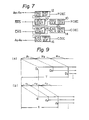
- Figure 7 is a more detailed block diagram of the arrangement of Fig. 1.
- the arrangement of Fig. 7 (Fig. 1) is used in a prior art semiconductor memory device.
- the second and third buffer control circuits 26 and 22 are not illustrated in Fig. 1 for simplification of the explanation regarding prior art
- Fig. 7 shows hardwares of 22 and 26 commonly exist in the prior art device.
- the series connection of the first and second buffer control circuits 24 and 26 is the most significant hardware characterising the present invention.
- Figure 8 is a block diagram representing a whole view of one example of the semiconductor memory device shown in Fig. 2 further provided with circuits 24 and 26 of Fig. 6, which circuits characterize the present invention.
- the operation of the circuit shown in Fig. 6 is as follows. With reference to Fig. 6 and also Fig. 4, first the column address enable signal S 1 is produced from the RAS part clock generator 10 and applied to the CAS part clock generator 14. The CAS part operation starts after activation of the RAS part operation. These operations are the same as those peformed in the aforementioned prior art semiconductor memory device. However, in the present invention, it is important to note that the timing control signals S 2 and S 3 of Fig. 6 are generated faster than the corresponding signals S 1 and S" of Fig. 1 in the prior art device. This is because the signals S 2 and S 3 are not derived from the column address enable signal S i , but from the RAS signa) itself, which occurs faster than the signal S l .
- the signal activating the buffer 16 of Fig. 1 is generated via the generator 14, while the signal activating the buffer 16 of Fig. 6 is not generated via such a generator 14. Consequently, the buffer 16 of Fig. 6 can be set in the enable state faster than the buffer 16 of Fig. 1.
- the timing control signal S 2 is directly derived from the buffer circuit 26 when it receives the RAS signa). In this case, the signal S 2 is generated after the reception of the RAS signal by 5 to 10 ns. Therefore, the buffer control circuit 26 and the column address buffer 16 can be set in the enable state even during the term t RAH (see Fig. 4). In the prior art, the circuit 26 and the buffer 16 cannot be set in the enable state until the term t RAH passes. Consequently, the CAS part can be active immediately after, first, the buffer control circuit 26 receives the timing control signal S 2 from the RAS part buffer control circuit 24 and, next, the address buffer 16 receives the timing control signal S 3 from the circuit 26. In this way, the term t AR can be shortened.
- the generation of the timing control signal S 2 should be faster than the occurrence of the trailing edge of the CAS signa).
- the occurrence of the trailing edge of the CAS signal can be variable in the range between the minimum and maximum values of the term t RCD' the generation of the signal S 2 should be faster than the minimum value of tRCD.
- the minimum value Of t RCD is, in the prior art, 50 ns, as shown in Fig. 5. That is, when t CAH is set to be 20 ns, the equation stands.
- FIG. 9 depicts timing charts used for schematically explaining the advantage of the present invention.
- reference symbols R1, R2, R3--- represent read cycles performed in respective memory blocks MB1, MB2, MB3--- (not shown).
- Reference symbols D1, D2, D3--- represent read data from the respective memory blocks.
- Figure 9(a) corresponds to a prior art.
- Fig. 9(a) corresponds to a prior art.
- reference symbols r1, r2, r3--- represent read cycles performed in respective memory blocks MB1, MB2, MB3--- (not shown).
- Reference symbols d1, d2, d3--- represent read data from the respective memory blocks.
- This figure 9(b) corresponds to the present invention.
- the read access time similar to write access time itself is the same in both Fig. 9(a) and Fig. 9(b)
- the time required for a series of data for example D1, D2, D3 (d1, d2, d3), is different.
- the required time is indicated as T in Fig. 9(a) and t in Fig. 9(b), where t obtained in the present invention is clearly shorter than T obtained in the prior art device.
- Figure 10 is a circuit diagram illustrating one example of the blocks 24 and 26 shown in Fig. 6.
- the buffer control circuit 24 is an inverter acting as a level converter.
- Figure 11 is a circuit diagram illustrating one example of the block 22 shown in Fig. 6.
- Figure 12 is a circuit diagram illustrating one example of the block 10 shown in Fig. 6.
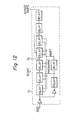
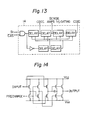
- Figure 13 is a circuit diagram illustrating one example of the block 14 shown in Fig. 6.
- Figure 14 is a circuit diagram illustrating one example of each delay circuit shown in Figs. 10, 11, 12, and 13.
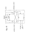
- Figure 15 is a circuit diagram illustrating one example of the block 16 shown in Fig. 6.
- the circuit construction of Fig. 15 is identical to the row address buffer 12 shown in Fig. 8.
Description
- The present invention relates to a semiconductor memory device, more particularly to a circuit for controlling a column part of the semiconductor memory device.
- In a typical semiconductor memory device, a write operation or a read operation is accomplished by first selecting the desired row line, that is, word line, and then selecting the desired column line, that is, bit line. This allows the selection of the memory cell located at the crossing point of the selected row and column lines and enables a write or read operation to be performed on that memory cell.
- Thus, write and read operations for the column and row lines do not occur simultaneously, but sequentially. In light of this sequential operation, a so-called address multiplex access method has been proposed, for example in United States of America Patent Specification
No 3 969 706. According to this method, first a row address strobe signal is externally supplied to the memory to establish a row access mode. Next a column address strobe signal is externally supplied to establish a column access mode. The column access mode starts when the column address strobe signal and a column address enable signal are both given. The column address enable signal is usually generated after certain processing is completed, which processing is started by receiving the row address strobe signal. - In this regard, the recent trend in semiconductor memory devices is toward very high speed read and write access operations. That is, the write or read access time must be as short as possible. In the prior art, there is a disadvantage in that the above-mentioned memory access operation cannot be conducted at a very high speed. This is because it takes a relatively long time to produce the aforementioned column address enable signal by the processing step initiated by the row address strobe signal.
- In accordance with this invention a semiconductor memory device comprising a row address buffer for receiving a row address signal when a row address strobe signal is externally supplied to the semiconductor memory device; a column address buffer for receiving a column address signal when a column address strobe signal is externally supplied to the semiconductor memory device; a row decoder and a column decoder cooperating with the row and column address buffers, respectively, and selecting the desired one of the memory cells specified by the row and column address signals; an RAS part clock generator producing a first timing control signal when the row address strobe signal is supplied, the first timing control signal being used for enabling the row part of the device; and, a CAS part clock generator producing a timing control signal for enabling the column decoder in the presence of both the column address strobe signal and the first timing control signal, is characterised by a circuit which detects and holds the row address strobe CAS signal and which enables the column address buffer, the circuit comprising a first buffer control circuit and a second buffer control circuit, the first buffer control circuit directly receiving the row address strobe
RAS signa! and producing a second timing control signal which is supplied to the second buffer control circuit, and the second buffer control circuit producing a third timing control signal which enables the column address buffer whilst the second buffer control circuit simultaneously receives both the second timing control signal and the column address strobe CAS signa!. - An example of a semiconductor memory device in accordance with this invention will now be described and contrasted with the prior art with reference to the accompanying drawings, in which:-
- Figure 1 is a block diagram of members for memory cell selection in a first prior art semiconductor memory device;
- Figure 2 is a block diagram of the whole of one example of a prior art semiconductor memory device using the selection arrangement shown in Figure 1;
- Figure 3 is a block diagram of members for memory cell selection in a second prior art semiconductor memory device;
- Figure 4 is a timing diagram illustrating the operation of the examples illustrated in Figures 1 and 2;
- Figure 5 is a graph showing the relationship between the terms tAR and TRCD;
- Figure 6 is a block diagram of a semiconductor memory device according to the present invention;
- Figure 7 is a more detailed block diagram of part of the prior art device shown in Figure 1;
- Figure 8 is a block diagram of the whole of the example of semiconductor memory device shown in Figure 2 when modified in accordance with the present invention;
- Figure 9 is a timing diagram illustrating the advantages of the present invention;
- Figure 10 is a circuit diagram of one example of the
blocks - Figure 11 is a circuit diagram of one example of the
block 22 shown in Figure 6; - Figure 12 is a circuit diagram of one example of the
block 10 shown in Figure 6; - Figure 13 is a circuit diagram of one example of the
block 14 shown in Figure 6; - Figure 14 is a circuit diagram of one example of each delay circuit shown in Figures 10, 11, 12 and 13; and,
- Figure 15 is a circuit diagram of one example of the
block 16 shown in Figure 6. - Figure 1 is a block diagram representing members for achieving memory cell selection in a prior art semiconductor memory device. As will be apparent hereinafter, the memory device of the present invention is based on the circuit arrangement shown in Fig. 1. In this figure, reference symbol RAS indicates the aforementioned row address strobe signal. The signal RAS is received by a RAS part clock generator (RAS PART CLK GEN) 10 which produces clocks used for carrying out various controls in the RAS part, such as an address fetch, a precharge of a row decoder, and a row line selection.
Reference numeral 12 represents a RAS part address buffer i.e., row address buffer, (RAS PART ADD BUF), which is triggered by a signal S' and brings the external row address Ao to A4 thereinto. Thereafter, thebuffer 12 supplies an address, which is an inverted row address of Ao to A4, to the row decoder (RDEC) (not shown in Fig. 1). Reference symbol CAS indicates the aforesaid column address strobe signal. The signalCAS is received by a CAS part clock generator (CAS PART CLK GEN) 14 which produces clocks used for carrying out various controls in the CAS part, such as identical to those mentioned above regarding the RAS part.Reference numeral 16 represents a CAS part address buffer (CAS PART ADD BUF), i.e., column address buffer, which is triggered by a timing control signal S" and brings the external column address A5 to Ag thereinto. Thereafter, thebuffer 14 supplies a column address to a column decoder (CDEC) (not shown in Fig. 1). It should be noted that the row address Ao to A4 and the column address As to Ag are applied to the same address input pins of the memory device, but alternatively. - Figure 2 is a block diagram representing a whole view of one example of a prior art semiconductor memory device employing the arrangement shown in Fig. 1. In Fig. 2, members the same as in Fig. 1 are represented by the same reference numerals or symbols.
- The block diagram of Fig. 2 may assist the understanding of the location of each member shown in Fig. 1 inside the semiconductor memory device.
- Figure 3 is a block diagram representing members, as in Fig. 1, for achieving another type of memory cell selection in a prior art semiconductor memory device. It is known that the arrangement of Fig. 3 is employed in a currently used Mostek type semiconductor memory device by Mostek Corporation of the U.S.A. In the arragement of Fig. 3, the RAS
part address buffer 12 and the CASpart address buffer 16, both shown in Figs. 1 and 2, are commonly realized by a single address buffer (ADD BUF) 18. Since the row and column address buffers are realized by onebuffer 18, the arrangement of Fig. 3 is advantageous from the viewpoint of pattern density in an integrated circuit (IC). However, the semiconductor memory device of the present invention is not based on such a common buffer type arrangement as in Fig. 3. In Fig. 3 and also Figs. 1 and 2, actually, inverted RAS and CAS signals are used. Therefore symbols RAS andCAS are used for the externally supplied row and column strobe signals, respectively. - Figure 4 is a timing diagram used for explaining the operations performed in Figs. 1 and 2. As seen from Fig. 4, the RAS signal is supplied first (see row (a)). When the level of the RAS signal changes from H (high) to L (low), the row address fetch operation becomes enable. Reference symbol tRAH see row (c)) represents a term in which the row address is held. Therefore, the term tRAH may be called a row address hold (RAH) term. Next, that is, after a term tRCD' the level of the
CAS signa! is changed to L (see row (b)), and thereby the column address fetch operation becomes enable. The term tRCD denotes a time delay from the row access to the column access. Reference symbol tCAH (see row (c)) represents a term in which the column address fetch operation is carried out. Therefore, the term tCAH may be called a column address hold (CAH) term. - Reference symbol WE denotes a write enable signal. Actually, an inverted signal of WE, that is, WE, is used as shown at the top right in Fig. 2. When the level of WE is high, the read operation cycle is maintained. If the level of WE is changed from H to L (see row (d)), this means that a write operation cycle is specified. The specifying of the write operation cycle commences after completion of the row address fetch operation and also immediately after the level change of
CAS from H to L. The write operation cycle is completed after the elapse of a write command hold (WCH) term tWCH (see row (d)). Specifically, the write operation is completed after the minimum term of tWCR (see row (e)), that is, tWCR min' and the minimum term of tWCH, that is, tWCH min' both elapse. The term tWCR min denotes the term from when the level ofRAS changes to L to when the specifying of the write operation cycle is released. The term tWCH min denotes the term from when the level ofCAS changes to L to when the specifying of the write operation cycle is released. - Reference symbol DIN denotes a write data, as shown at the center right of Fig. 2. The level change of DIN is shown in row (e) of Fig. 4. In row (e), reference symbol tDH denotes the term for holding the input write data D,N. The term tDHR is equal to the sum of tRCD max and tDH. The term tAR is equal to the sum of tRCD and tcAH.
- In the above-mentioned semiconductor memory device, which is fabricated as a metal- oxide semiconductor (MOS) memory and operated under the aforesaid address multiplex access method, the trailing edge of the
RAS signal and the trailing edge of the CAS signal must be shifted in time with each other so as to avoid row and column address fetch operation error. That is, first, the term tRAH is given for sufficiently holding the row address (Ao-A4). After the elapse of the term TRAH, the row address (Ao~A4) is switched in an address bus AB (see bottom left in Fig. 2) to the column address (A5~A9). If the switching term from the row address to the column address is represented by symbol 6 (see row (c) in Fig. 4), the trailing edge of the CAS signal must occur later than the trailing edge of the RAS signal, where the equation of
- Figure 5 is a graph represeting the relationship between the terms tAR and tRCD' both shown in Fig. 4. The relationship between tAR and TRCD in the prior art semiconductor memory device is schematically represented by the characteristic curve shown by bent solid lines C, and C'1. It should be understood that each value of time is recited merely as an example. As seen from the graph, the term tAR is proportional to the term tRCD when the term tRCD is relatively long (refer to line C1). However, when the term tRCD is shorter than a predetermined value of tRCD max (about 50 ns), the value of tAR is maintained at a fixed value (70 ns) defined by the predetermined value (50 ns) of tRCD mox and, thus, the value of tAR can no longer be shorter than the fixed value (refer to line Cl).
- The reason for this is as follows. With reference to Figs. 1, 2, and 4 again, the CAS
part clock generator 14 is not driven until an AND logic between S, and CAS is satisfied, in which the signal S, is the aforesaid column address enable signal produced from the RASpart clock generator 10. In other words, the CASpart clock generator 14 starts operating when both the signal S1 and CAS are applied thereto. The column address enable signal S, is, in Fig. 5, generated at about the 50 ns time, which is defined as the term tRCD max. The term tRCDmax is the maximum value of the time delay from the change of RAS to the change ofCAS and, at the same time, is the value sufficient for maintaining the minimum value of the term tAR, i.e., tARmin. To be more specific, if the column address enable signal S, is applied faster than the end of the term tRCD min to the CASpart clock generator 14, thegenerator 14 can start operating at the same time as the arrival of the CAS signal. - Soon after this, the
column address buffer 16 starts operating by receiving an output clock (refer to S" in Fig. 1) produced from thegenerator 14, now operating. Accordingly, the term TCAH (see row (c) in Fig. 4) can be quickly started. Contrary to the above, if the column address enable signal S, is applied later than the end of the term tRCD min to the CASpart clock generator 14, thegenerator 14 cannot start operating until the S1 signal is supplied. Therefore, thecolumn address buffer 16 waits for the arrival of the signal S1 and starts operating thereafter. Thus, the value of the term tAR min is larger than the sum of the values of the terms tRCD min and TCAH. - As mentioned above, in the prior art semiconductor memory device, the term tAR in row (c) of Fig. 4 necessarily becomes relatively long.
- Figure 6 is a block diagram of a semiconductor memory device according to an embodiment of the present invention. In Fig. 6, members the same as those of Figs. 1 and 2 are represented by the same reference numerals or symbols.
- The essential feature of the present invention resides in the fact that a certain means is newly employed, that is, a means for detecting and holding the row address strobe signal RAS so as to quickly produce a timing control signal (corresponding to S" in Fig. 1) to be supplied to the
column address buffer 16. The above-mentioned means is constructed by for example, a firstbuffer control circuit 24, a secondbuffer control circuit 26, and a thirdbuffer control circuit 22. The thirdbuffer control circuit 22 cooperates with therow address buffer 12. The firstbuffer control circuit 24 receives theRAS signal and controls the secondbuffer control circuit 26. The secondbuffer control circuit 26 controls thecolumn address buffer 16. The firstbuffer control circuit 24 directly receives the RAS signal and produces a column address enable signal S2 to be applied to the secondbuffer control circuit 26, the second buffer control circuit producing a signal S3 to be applied to thecolumn address buffer 16. Among these buffer control circuits, the second and thirdbuffer control circuits - Figure 7 is a more detailed block diagram of the arrangement of Fig. 1. The arrangement of Fig. 7 (Fig. 1) is used in a prior art semiconductor memory device. Although the second and third
buffer control circuits buffer control circuits - Figure 8 is a block diagram representing a whole view of one example of the semiconductor memory device shown in Fig. 2 further provided with
circuits - The operation of the circuit shown in Fig. 6 is as follows. With reference to Fig. 6 and also Fig. 4, first the column address enable signal S1 is produced from the RAS
part clock generator 10 and applied to the CASpart clock generator 14. The CAS part operation starts after activation of the RAS part operation. These operations are the same as those peformed in the aforementioned prior art semiconductor memory device. However, in the present invention, it is important to note that the timing control signals S2 and S3 of Fig. 6 are generated faster than the corresponding signals S1 and S" of Fig. 1 in the prior art device. This is because the signals S2 and S3 are not derived from the column address enable signal Si, but from theRAS signa) itself, which occurs faster than the signal Sl. In other words, the signal activating thebuffer 16 of Fig. 1 is generated via thegenerator 14, while the signal activating thebuffer 16 of Fig. 6 is not generated via such agenerator 14. Consequently, thebuffer 16 of Fig. 6 can be set in the enable state faster than thebuffer 16 of Fig. 1. - According to the above operations of the present invention, when the level of the CAS signal changes to L, various operations, such as the column address fetch, the write command fetch, and input write data fetch operations, can be started immediately after a predetermined column address holding term. In other words, the CAS part operation can always be activated by the CAS signal, therefore, the equation

- Taking experimental values as an example, in the present invention, when tRAH=15 ns and 5=10 ns, tRCD can be reduced to 25 ns. However, in the prior art memory device, the minimum value of tRCD is fixed at 50 ns. To be specific, with reference to Fig. 7, according to the prior art arrangement, the signal S1 from the RAS
part clock generator 10 is to be applied to thebuffer control circuit 26 and, thereafter, thecolumn address buffer 16 can be brought in an enable state by an output signal from thecircuit 26. Accordingly, it is required to set the term tRCD (see Fig. 4) as long as possible. This results in the term tAR becoming unnecessarily long. However, according to the present invention, as seen from Fig. 6, the timing control signal S2 is directly derived from thebuffer circuit 26 when it receives theRAS signa). In this case, the signal S2 is generated after the reception of the RAS signal by 5 to 10 ns. Therefore, thebuffer control circuit 26 and thecolumn address buffer 16 can be set in the enable state even during the term tRAH (see Fig. 4). In the prior art, thecircuit 26 and thebuffer 16 cannot be set in the enable state until the term tRAH passes. Consequently, the CAS part can be active immediately after, first, thebuffer control circuit 26 receives the timing control signal S2 from the RAS partbuffer control circuit 24 and, next, theaddress buffer 16 receives the timing control signal S3 from thecircuit 26. In this way, the term tAR can be shortened. Further, since the CAS part operation is controlled in timing by the CAS signal, the equation
- The generation of the timing control signal S2 should be faster than the occurrence of the trailing edge of the
CAS signa). In this case, since the occurrence of the trailing edge of the CAS signal can be variable in the range between the minimum and maximum values of the term tRCD' the generation of the signal S2 should be faster than the minimum value of tRCD. The minimum value Of tRCD is, in the prior art, 50 ns, as shown in Fig. 5. That is, when tCAH is set to be 20 ns, the equation
- The essential advantage of the present invention is that the cycle time of a memory can be shortened, because the address hold time can be minimized. This advantage is remarkable when the semiconductor memory devices of the present invention are operated under a so-called interleave mode. This will be clarified with reference to Fig. 9. Figure 9 depicts timing charts used for schematically explaining the advantage of the present invention. In Fig. 9(a), reference symbols R1, R2, R3--- represent read cycles performed in respective memory blocks MB1, MB2, MB3--- (not shown). Reference symbols D1, D2, D3--- represent read data from the respective memory blocks. Figure 9(a) corresponds to a prior art. In Fig. 9(b), reference symbols r1, r2, r3--- represent read cycles performed in respective memory blocks MB1, MB2, MB3--- (not shown). Reference symbols d1, d2, d3--- represent read data from the respective memory blocks. This figure 9(b) corresponds to the present invention. As apparent from Fig. 9, although the read access time similar to write access time itself is the same in both Fig. 9(a) and Fig. 9(b), the time required for a series of data, for example D1, D2, D3 (d1, d2, d3), is different. The required time is indicated as T in Fig. 9(a) and t in Fig. 9(b), where t obtained in the present invention is clearly shorter than T obtained in the prior art device.
- Finally, a detailed example of each block shown in Fig. 6 will be disclosed. Figure 10 is a circuit diagram illustrating one example of the
blocks buffer control circuit 24 is an inverter acting as a level converter. Figure 11 is a circuit diagram illustrating one example of theblock 22 shown in Fig. 6. Figure 12 is a circuit diagram illustrating one example of theblock 10 shown in Fig. 6. Figure 13 is a circuit diagram illustrating one example of theblock 14 shown in Fig. 6. Figure 14 is a circuit diagram illustrating one example of each delay circuit shown in Figs. 10, 11, 12, and 13. Figure 15 is a circuit diagram illustrating one example of theblock 16 shown in Fig. 6. The circuit construction of Fig. 15 is identical to therow address buffer 12 shown in Fig. 8.
Claims (6)
Applications Claiming Priority (2)
| Application Number | Priority Date | Filing Date | Title |
|---|---|---|---|
| JP194200/81 | 1981-12-02 | ||
| JP56194200A JPS6052513B2 (en) | 1981-12-02 | 1981-12-02 | semiconductor storage device |
Publications (3)
| Publication Number | Publication Date |
|---|---|
| EP0080902A2 EP0080902A2 (en) | 1983-06-08 |
| EP0080902A3 EP0080902A3 (en) | 1983-09-28 |
| EP0080902B1 true EP0080902B1 (en) | 1985-11-21 |
Family
ID=16320613
Family Applications (1)
| Application Number | Title | Priority Date | Filing Date |
|---|---|---|---|
| EP82306384A Expired EP0080902B1 (en) | 1981-12-02 | 1982-12-01 | Semiconductor memory device |
Country Status (5)
| Country | Link |
|---|---|
| US (1) | US4602356A (en) |
| EP (1) | EP0080902B1 (en) |
| JP (1) | JPS6052513B2 (en) |
| DE (1) | DE3267623D1 (en) |
| IE (1) | IE54281B1 (en) |
Families Citing this family (12)
| Publication number | Priority date | Publication date | Assignee | Title |
|---|---|---|---|---|
| US4596004A (en) * | 1983-09-14 | 1986-06-17 | International Business Machines Corporation | High speed memory with a multiplexed address bus |
| IT1181168B (en) * | 1984-03-02 | 1987-09-23 | Zanussi Zeltron Inst | MEMORY COMPONENT AND MEMORY PLATE MANAGEMENT PROCEDURE USING SUCH PROCEDURE |
| DE3780551T2 (en) * | 1986-09-04 | 1993-03-11 | Fujitsu Ltd | STORAGE DEVICE USING ADDRESS MULTIPLEX. |
| JPS63225836A (en) * | 1987-03-13 | 1988-09-20 | Brother Ind Ltd | Storage device |
| US5031150A (en) * | 1988-08-26 | 1991-07-09 | Kabushiki Kaisha Toshiba | Control circuit for a semiconductor memory device and semiconductor memory system |
| JP2646032B2 (en) * | 1989-10-14 | 1997-08-25 | 三菱電機株式会社 | LIFO type semiconductor memory device and control method therefor |
| JP2744115B2 (en) * | 1990-05-21 | 1998-04-28 | 株式会社東芝 | Control circuit of pseudo static RAM |
| DE69126253D1 (en) * | 1990-06-29 | 1997-07-03 | Ibm | Dynamic random memory with high speed and extended reset / precharge time |
| US5270970A (en) * | 1991-03-15 | 1993-12-14 | Motorola, Inc. | Memory device having a buffer for gating data transmissions |
| JP2871967B2 (en) * | 1991-08-20 | 1999-03-17 | 日本電気アイシーマイコンシステム株式会社 | Dual-port semiconductor memory device |
| US6072746A (en) * | 1998-08-14 | 2000-06-06 | International Business Machines Corporation | Self-timed address decoder for register file and compare circuit of a multi-port CAM |
| US6477630B2 (en) | 1999-02-24 | 2002-11-05 | International Business Machines Corporation | Hierarchical row activation method for banking control in multi-bank DRAM |
Citations (1)
| Publication number | Priority date | Publication date | Assignee | Title |
|---|---|---|---|---|
| US3969706A (en) * | 1974-10-08 | 1976-07-13 | Mostek Corporation | Dynamic random access memory misfet integrated circuit |
Family Cites Families (4)
| Publication number | Priority date | Publication date | Assignee | Title |
|---|---|---|---|---|
| JPS546429A (en) * | 1977-06-16 | 1979-01-18 | Toshiba Corp | Semiconductor memory device |
| JPS586231B2 (en) * | 1977-07-04 | 1983-02-03 | 富士通株式会社 | Driving method of semiconductor memory device |
| JPS5951073B2 (en) * | 1980-03-27 | 1984-12-12 | 富士通株式会社 | semiconductor storage device |
| JPS6012718B2 (en) * | 1980-03-28 | 1985-04-03 | 富士通株式会社 | semiconductor dynamic memory |
-
1981
- 1981-12-02 JP JP56194200A patent/JPS6052513B2/en not_active Expired
-
1982
- 1982-12-01 DE DE8282306384T patent/DE3267623D1/en not_active Expired
- 1982-12-01 EP EP82306384A patent/EP0080902B1/en not_active Expired
- 1982-12-01 IE IE2856/82A patent/IE54281B1/en not_active IP Right Cessation
- 1982-12-01 US US06/445,921 patent/US4602356A/en not_active Expired - Lifetime
Patent Citations (1)
| Publication number | Priority date | Publication date | Assignee | Title |
|---|---|---|---|---|
| US3969706A (en) * | 1974-10-08 | 1976-07-13 | Mostek Corporation | Dynamic random access memory misfet integrated circuit |
Also Published As
| Publication number | Publication date |
|---|---|
| EP0080902A2 (en) | 1983-06-08 |
| US4602356A (en) | 1986-07-22 |
| JPS5897182A (en) | 1983-06-09 |
| IE822856L (en) | 1983-06-02 |
| IE54281B1 (en) | 1989-08-16 |
| DE3267623D1 (en) | 1986-01-02 |
| JPS6052513B2 (en) | 1985-11-19 |
| EP0080902A3 (en) | 1983-09-28 |
Similar Documents
| Publication | Publication Date | Title |
|---|---|---|
| KR100256308B1 (en) | Optimization circuitry and control for a synchronous memory device with programmable latency period | |
| US7327613B2 (en) | Input circuit for a memory device | |
| KR100915554B1 (en) | A semiconductor memory | |
| US6243797B1 (en) | Multiplexed semiconductor data transfer arrangement with timing signal generator | |
| US6002615A (en) | Clock shift circuit and synchronous semiconductor memory device using the same | |
| EP0080902B1 (en) | Semiconductor memory device | |
| US6160754A (en) | Synchronous memory device of a wave pipeline structure | |
| EP0773549B1 (en) | Synchronous semiconductor memory having a write execution time dependent upon a cycle time | |
| JPS61105795A (en) | Memory circuit | |
| US5802596A (en) | High speed synchronous DRAM having a pipeline structure | |
| US6693844B2 (en) | Sending signal through integrated circuit during setup time | |
| US6166970A (en) | Priority determining apparatus using the least significant bit and CAS latency signal in DDR SDRAM device | |
| US6463007B2 (en) | Synchronous semiconductor memory device | |
| EP0766251A2 (en) | Semiconducteur memory device having extended margin in latching input signal | |
| KR100324143B1 (en) | Semiconductor memory device and method of burn-in testing | |
| KR100486195B1 (en) | Auto precharge control circuit of synchronous dram | |
| EP0782143A2 (en) | A semiconductor memory circuit equipped with a column addressing circuit having a shift register | |
| JP3097301B2 (en) | Semiconductor memory device | |
| JPH1092175A (en) | Cas signal generator of synchronous dram | |
| KR100623948B1 (en) | Semiconductor memory and method of operating same | |
| KR950003401B1 (en) | Device which generates column address latch signal | |
| US6704243B2 (en) | Apparatus for generating memory-internal command signals from a memory operation command | |
| KR100318323B1 (en) | Address signal generator of semiconductor memory | |
| JP3125685B2 (en) | Synchronous semiconductor memory device | |
| JPH02214094A (en) | Semiconductor memory |
Legal Events
| Date | Code | Title | Description |
|---|---|---|---|
| PUAI | Public reference made under article 153(3) epc to a published international application that has entered the european phase |
Free format text: ORIGINAL CODE: 0009012 |
|
| AK | Designated contracting states |
Designated state(s): DE FR GB |
|
| PUAL | Search report despatched |
Free format text: ORIGINAL CODE: 0009013 |
|
| AK | Designated contracting states |
Designated state(s): DE FR GB |
|
| 17P | Request for examination filed |
Effective date: 19831018 |
|
| GRAA | (expected) grant |
Free format text: ORIGINAL CODE: 0009210 |
|
| AK | Designated contracting states |
Designated state(s): DE FR GB |
|
| REF | Corresponds to: |
Ref document number: 3267623 Country of ref document: DE Date of ref document: 19860102 |
|
| ET | Fr: translation filed | ||
| PLBE | No opposition filed within time limit |
Free format text: ORIGINAL CODE: 0009261 |
|
| STAA | Information on the status of an ep patent application or granted ep patent |
Free format text: STATUS: NO OPPOSITION FILED WITHIN TIME LIMIT |
|
| 26N | No opposition filed | ||
| PGFP | Annual fee paid to national office [announced via postgrant information from national office to epo] |
Ref country code: GB Payment date: 20011205 Year of fee payment: 20 |
|
| PGFP | Annual fee paid to national office [announced via postgrant information from national office to epo] |
Ref country code: FR Payment date: 20011212 Year of fee payment: 20 |
|
| PGFP | Annual fee paid to national office [announced via postgrant information from national office to epo] |
Ref country code: DE Payment date: 20011217 Year of fee payment: 20 |
|
| REG | Reference to a national code |
Ref country code: GB Ref legal event code: IF02 |
|
| PG25 | Lapsed in a contracting state [announced via postgrant information from national office to epo] |
Ref country code: GB Free format text: LAPSE BECAUSE OF EXPIRATION OF PROTECTION Effective date: 20021130 |
|
| REG | Reference to a national code |
Ref country code: GB Ref legal event code: PE20 Effective date: 20021130 |