EP0077118A1 - Motor power factor controller with a reduced voltage starter - Google Patents
Motor power factor controller with a reduced voltage starter Download PDFInfo
- Publication number
- EP0077118A1 EP0077118A1 EP82303963A EP82303963A EP0077118A1 EP 0077118 A1 EP0077118 A1 EP 0077118A1 EP 82303963 A EP82303963 A EP 82303963A EP 82303963 A EP82303963 A EP 82303963A EP 0077118 A1 EP0077118 A1 EP 0077118A1
- Authority
- EP
- European Patent Office
- Prior art keywords
- signal
- power factor
- motor
- phase
- output
- Prior art date
- Legal status (The legal status is an assumption and is not a legal conclusion. Google has not performed a legal analysis and makes no representation as to the accuracy of the status listed.)
- Granted
Links
Images


Classifications
-
- H—ELECTRICITY
- H02—GENERATION; CONVERSION OR DISTRIBUTION OF ELECTRIC POWER
- H02P—CONTROL OR REGULATION OF ELECTRIC MOTORS, ELECTRIC GENERATORS OR DYNAMO-ELECTRIC CONVERTERS; CONTROLLING TRANSFORMERS, REACTORS OR CHOKE COILS
- H02P1/00—Arrangements for starting electric motors or dynamo-electric converters
- H02P1/16—Arrangements for starting electric motors or dynamo-electric converters for starting dynamo-electric motors or dynamo-electric converters
- H02P1/26—Arrangements for starting electric motors or dynamo-electric converters for starting dynamo-electric motors or dynamo-electric converters for starting an individual polyphase induction motor
- H02P1/28—Arrangements for starting electric motors or dynamo-electric converters for starting dynamo-electric motors or dynamo-electric converters for starting an individual polyphase induction motor by progressive increase of voltage applied to primary circuit of motor
-
- H—ELECTRICITY
- H02—GENERATION; CONVERSION OR DISTRIBUTION OF ELECTRIC POWER
- H02J—CIRCUIT ARRANGEMENTS OR SYSTEMS FOR SUPPLYING OR DISTRIBUTING ELECTRIC POWER; SYSTEMS FOR STORING ELECTRIC ENERGY
- H02J3/00—Circuit arrangements for ac mains or ac distribution networks
- H02J3/18—Arrangements for adjusting, eliminating or compensating reactive power in networks
- H02J3/1892—Arrangements for adjusting, eliminating or compensating reactive power in networks the arrangements being an integral part of the load, e.g. a motor, or of its control circuit
-
- H—ELECTRICITY
- H02—GENERATION; CONVERSION OR DISTRIBUTION OF ELECTRIC POWER
- H02P—CONTROL OR REGULATION OF ELECTRIC MOTORS, ELECTRIC GENERATORS OR DYNAMO-ELECTRIC CONVERTERS; CONTROLLING TRANSFORMERS, REACTORS OR CHOKE COILS
- H02P23/00—Arrangements or methods for the control of AC motors characterised by a control method other than vector control
- H02P23/26—Power factor control [PFC]
-
- H—ELECTRICITY
- H02—GENERATION; CONVERSION OR DISTRIBUTION OF ELECTRIC POWER
- H02P—CONTROL OR REGULATION OF ELECTRIC MOTORS, ELECTRIC GENERATORS OR DYNAMO-ELECTRIC CONVERTERS; CONTROLLING TRANSFORMERS, REACTORS OR CHOKE COILS
- H02P2201/00—Indexing scheme relating to controlling arrangements characterised by the converter used
- H02P2201/15—Power factor Correction [PFC] circuit generating the DC link voltage for motor driving inverter
Definitions
- This invention relates to a power factor input control for an induction motor incorporating a reduced voltage starting capability.
- Applicant's U.S. Patent No. 4,052,648 discloses a power reduction system for induction motors in which the operating power factor of a motor is monitored, and the effective voltage input to the motor is controlled as a function of the difference between a commanded power factor signal and the operating power factor.
- Applicant's European patent application published in Bulletin 82/20 under No. 0051903 discloses a power factor type control system particularly adapted for three-phase induction motors.
- signal means are provided which initially block the application of the normal or "run" power factor command signal, and by means of a ramp signal generator, there is provided an increasing, with time, voltage in place of that command signal.
- This increase in voltage is of an amplitude and rate which will effect a graduated turn-on of the thyristor(s) of the motor circuit, effecting a full turn-on in a selected period of typically 5 to 30 seconds.
- a comparator examines the ramp voltage, and when the ramp voltage has risen sufficiently to effect a full turn-on of the thyristors and full motor operating speed, the comparator provides a signal which unblocks the normal power factor command signal, enabling the turn-on of a thyristor or thyristors to thereafter be determined by motor loading in a conventional manner for a power factor type controller.
- a three phase induction motor 10 is powered through thyristor or SCR (silicon control rectifier) devices 12, 14, and 16 from a three phase power line, typically providing 220 or 440 volts, 60 cycle, alternating current to terminals A, B, and C.
- SCR silicon control rectifier
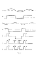
- One phase of such a signal is illustrated by voltage waveform a of Figure 3.
- SCR devices provide for conduction only in one direction
- a diode 18 is connected across each SCR and poled for opposite direction conduction.
- Current is sampled by current sampling transformers 26, 28, and 30, shunted by resistors 20, 22, and 24, each of these resistors being connected in series with an input to motor 10.
- Transformers 26, 28, and 30 are individually connected across one of these resistors (via a primary winding, as shown), and with one secondary terminal grounded, the other secondary terminal provides a discretely phased current signal output (as shown in waveform c of Figure 3).
- Terminal X is associated with phase A
- terminal Z is associated with phase C
- terminal Y is associated with phase B.
- a power factor signal inversely proportional to the current-voltage phase differential of each of the three phase inputs is obtained, separately, by phase detectors 32', 34, and 36.
- Phase detector 32 receives a current responsive signal sample from terminal Z representative of the C phase current, and a voltage signal from transformer 38 representative of the A-C phase voltage, and provides a first phase detected output at terminal 40.
- Phase detector 34 receives a sample from terminal Y representative of the B phase current and a C-B phase voltage sample from transformer 42, and provides a second phase detected output at terminal 40.
- Phase detector 36 receives a phase A current signal'sample from terminal X and a B-A phase voltage sample from transformer 44, and provides a third phase detection signal at terminal 40.
- the three signals, designated P 1 , P 2 , and P 3 , respectively, from the three phase detectors are shown in waveforms f and g of Figure 3.
- the phase detectors are identical; one is shown in Figure 2. It includes two conventional squaring circuits. One is voltage square wave shaper 50, which provides through resistor 52 a rectangular wave (waveform b of Figure 3) responsive to the input voltage (waveform a of Figure 3). The second one is current square wave shaper 56, which provides through resistor 54 a rectangular wave (waveform d of Figure 3) representative of the negative half cycle of input current (waveform c of Figure 3). The outputs of the two wave shaping circuits are combined through resistors 52 and 54. Diode 60 passes only the positive portion of each output to terminal 40, which is common to the outputs of all three phase detectors.
- Waveform e illustrates the combination process showing the waveform of a single phase detector as it would appear without diode 60, which diode eliminates the negative portions of the waveforms.
- each phase detector produces a pulse (e.g., P I from detector 32, P 2 from detector 34, and P 3 from detector 36) which is, in effect, turned “on” by the leading or rising edge of voltage waveform b and turned “off” by the trailing edge of waveform d.
- the width of pulse P I (it has a constant amplitude) tends to increase with an increase phase angle between current and voltage (thus decreased power factor) and decrease in width with decreased phase angle (and thus increased power factor).
- waveforms f and g illustrate the relative time presence of output pulses P 2 and P 3 from phase detectors 34 and 36, respectively.
- waveform g of Figure 3 illustrates the combined signals at this point.
- This composite becomes the basic feedback control signal, and as will be noted, this is a signal of pulses of a repetition rate of 180 Hz. This is in contrast to previous circuit approaches wherein a single phase detected output (from one of the three phases) is employed, which would, of course, have been either at 60 Hz or 120 Hz rate, depending upon whether a half or full wave detection was employed.
- the next step in accordance with this invention is to effect a conditioning of the control signal wherein its direct current characteristic must be compatible with the SCR trigger circuitry and still have a frequency response up to on the order of 20 Hz.
- the control signal is applied to the inverting input of operational amplifier 64 of signal conditioner or integrating circuit 66, together with a power factor command signal supplied through resistor 68 and 69 from potentiometer 70.
- Potentiometer 70 is biased negatively to provide a difference or subtraction signal with respect to the positive signal as developed at the outputs of the phase detectors.
- Signal conditioning is effected by an inverse feedback network consisting of two circuits, one being capacitor 72 connected between the output and inverting input of operational amplifier 64, and the other consisting of a series combination of capacitor 74 and resistor 76 connected between these two points.
- the feedback network is basically an integrative or lag one.
- the combination of resistor 76 (approximately 15,000 ohms) and capacitor 74 (approximately 5 MFD) is initially effective (at 0 frequency) to commence providing a lag effect. At about 2 Hz, the lag state commences to diminish as the value of resistor 76 commences to have a dominant effect over capacitor 74.
- capacitor 72 (approximately .68 MFD) commences to be effective to again impose a pronounced lag effect.
- the resulting signal is a relatively smooth signal representing the integral of the composite outputs of the phase detectors less the command signal.
- the signal as used, is represented by the sample signal waveforms 8 1 and S 2 as shown in Figure 4. It is important that while the signals have a relatively smooth and constant level, approximating the average signal value present, the signal must be responsive to signal changes incident to changes in motor loading, typically calling for a signal response upward to approximately 20 Hz. This is achieved by the circuitry as shown.
- the circuitry thus far described was designed to develop a control signal for regulating the input power to motor 10 once the motor was started.
- the present invention is particularly directed to developing a signal for controlling the application of power to motor 10 during the period from the instant when power is turned “on” for a discrete selected interval of typically 5 to 30 seconds, during which the motor will have increased to operating speed.
- the purpose of this invention, as described above, is to prevent abrupt surges in input current which are not necessary for starting the motor, without accompanying instabilities.
- circuitry is added which provides a substitute command signal to that provided by potentiometer 70 during the start-up interval.
- operational amplifier 64 which processes control signals, is initially disabled for approximately 100 milliseconds. As operational control signals are applied to the inverting input of operational amplifier 64, and are negative going to provide turn-on signals for the thyristors, a counter or disabling signal is applied to its non-inverting input. This is accomplished by applying a -15 volts to capacitor 77, which is in series with resistor 78, in turn connected between the non-inverting input of amplifier 64 and ground. The time constant of this circuit is adjusted to effect signal blocking for the period described.
- the output of thyristor trigger oscillator 102 is initially blocked by NPN transistor 150 connected through output resistor 152 across the output of oscillator 102.
- Transistor 150 is initially turned “on”, shorting the output of oscillator 102, by a declining ramp signal appearing across resistor 154 in series with capacitor 156 and a +15 volts source.
- the time constant provided by resistor 154 and capacitor 156 is such that transistor 150 would be essentially discharged in approximately 10 milliseconds, after which the blocking action would cease and transistor 150 would be turned “off”, enabling a normal output from oscillator 102.
- the bias to the non-inverting input is a fixed bias, being a selected fraction of -15 volts as provided by a voltage divider comprising resistors 164 and 166 and connected across the -15 volts as shown. Initially, the voltage applied to the inverting input of operational amplifier 162 is zero, the initial output of operational amplifier 182, and thus the potential on the non-inverting input of operational amplifier 162 prevails.
- Potentiometer 168 through resistor 170, provides an initial starting level negative signal to terminal 172 where it is added to a negative going, start-up, ramp signal supplied from the output of starting ramp generator 174 through resistor 176.
- NPN transistor 178 is connected emitter-to-collector between terminal 172 and ground and blocks an interfering effect from a starting signal after the starting sequence. Transistor 178 is controlled by an output through resistor 180 from operational amplifier 162, and is initially held “off” during the starting sequence by the negative output of operational amplifier 162.
- Starting ramp generator 174 is a conventional integrator comprising operational amplifier 182 and a capacitor 184 connected from its-output to its inverting input.
- a selected positive bias is obtained from potentiometer 186, connected between the +15 volts terminal and ground. This bias is fed through input resistor 192 to the inverting input of operational amplifier 182. The result is that, upon the application of voltages to the circuit, there will initially occur at the output of operational amplifier 182 an essentially zero voltage which ramps down negatively at a selected rate determined by this bias and the time constant of capacitor 184 and input resistor 192 to achieve a desired rate of motor turn "on" signal.
- the negative going signal at the output of operational amplifier 182 is fed through resistor 176 to terminal 172 and there added to a voltage from potentiometer 168, fed through resistor 170. This signal is then applied through resistor 183 to terminal 40 and there summed with the operating power factor (or current-voltage phase angle) signal and applied to'operational amplifier 64 to effect an increasing (negatively) control signal which gradually, over a typical period of 5 to 30 seconds, results in effective motor voltage to be raised to full voltage.
- the actual operational control effected by the control signal on the thyristors is discussed below.
- the output of operational amplifier 182 is also applied, in this case, to the inverting input of operational amplifier 162; and when the output rises to a level which exceeds the level applied to the non-inverting input of operational amplifier 162, the output of the latter switches from a negative state to a positive state.
- This changed state is fed as a switching potential to transistors 178 and 158 to turn transistor 178 "on” and transistor 158 "off".
- transistor 178 prevents any further starting signal from appearing at terminal 172, and transistor 158 unblocks the output of potentiometer 70 to restore normal power factor control for "run" operation of motor 10.
- Actual thyristor triggering signals are developed by the comparison of the control signal (e.g., S 1 and S 2 of Figure 4) output of operational amplifier 64 and ramp shaped signals r.
- a ramp signal for each phase is developed by one of conventional ramp generators 84, 86, and 88, responsive to A-C, C-B, and B-A phase voltages from transformers 38, 42, and 44, respectively.
- the ramp outputs r of these generators are illustrated by solid line in waveforms a, b, and c, respectively, of Figure 4 and are separately applied to conventional comparators 90, 92, and 94, together with a control signal from operational amplifier 64.
- a comparator provides a pulse output when the level of the control signal, e.g., dashed line S 1 of Figure 4, intersects the leading edge of a ramp signal.
- a control signal S 1 applied to the comparators output pulses are produced as shown in waveforms d, e, and f of Figure 4. These pulses, which result in the triggering of the thyristors, occur one per cycle, and are thus representative of a half wave mode of operation.
- the relatively narrow triggering pulses shown as waveforms d, e, and f produce relatively short turn-on times for SCR devices 12, 14, and 16, and thus produce a relatively low RMS input voltage to motor 10.
- phase detectors detecting a downward shift in power factor (by an upward shift in current-voltage phase angle) occurring when motor loading is reduced.
- the resulting output signal of operational amplifier 64 will produce a motor RMS input voltage which brings about an equilibrium between the commanded power factors determined by the bias output of potentiometer 70 and integrated output of the phase detectors.
- the actual control of the current turn-on periods for the thyristors is effected by gates 96, 98, and 100, which pass high frequency signals responsive to the outputs of the comparators. These gates are electronic switches and function to gate the high frequency signal (e.g., 10 KHz) from oscillator 102 through the primary windings of transformers 104, 106, and 108 to the thyristors. Resistor 110 and diode 112 are connected in series across the primary of each transformer to suppress inductive voltages to a safe level consistentwith the semi-conductive circuitry employed. The secondaries of transformers 104, 106, and 108 are connected in series with diode 114 between the gate and cathode of SCR devices 12, 14, and 16.
- the turn-on periods for the thyristors follow the periods of the pulse outputs of the comparators (as shown in waveforms d-i).
- the waveforms g-i, which are produced by control signal S 2 are illustrative of the turn-on periods for a moderately to heavily loaded motor in contrast to waveforms d-f which are indicative of a slightly loaded or unloaded motor:
- Figure 1 illustrates a three-phase system employing SCR devices as thyristors in a basically half wave control system
- the invention is also applicable to full wave three-phase systems employing either triacs or SCR devices connected in anti-parallel.
Landscapes
- Engineering & Computer Science (AREA)
- Power Engineering (AREA)
- Motor And Converter Starters (AREA)
- Control Of Ac Motors In General (AREA)
- Control Of Motors That Do Not Use Commutators (AREA)
- Control Of Eletrric Generators (AREA)
Abstract
Description
- This invention relates to a power factor input control for an induction motor incorporating a reduced voltage starting capability.
- Applicant's U.S. Patent No. 4,052,648 discloses a power reduction system for induction motors in which the operating power factor of a motor is monitored, and the effective voltage input to the motor is controlled as a function of the difference between a commanded power factor signal and the operating power factor. Applicant's European patent application published in Bulletin 82/20 under No. 0051903 discloses a power factor type control system particularly adapted for three-phase induction motors.
- In addition to minimizing motor power consumption during normal running conditions, a second area of concern is that of current surges which occur when a motor is first turned on. These surges can amount to five to eight times the normal operating current, and are both wasteful of electrical power and can contribute to excessive load surcharges being borne by electrical users. While discrete starting circuits have been employed which ideally gradually apply a starting voltage, it has been found that in some instances these circuits fail to provide a smooth start-up, and not infrequently there may occur significant motor vibrations during at least a portion of the start-up interval.
- It is the object of this invention to provide a single control system which both regulates power usage during normal running of a motor and provides for a graduated turn-on of motor voltage without the attendant problem of motor vibration. It is a particular object of the invention to provide a system of this category for a three-phase motor where graduated voltage starting circuits are most frequently used.
- In accordance with this invention, signal means are provided which initially block the application of the normal or "run" power factor command signal, and by means of a ramp signal generator, there is provided an increasing, with time, voltage in place of that command signal. This increase in voltage is of an amplitude and rate which will effect a graduated turn-on of the thyristor(s) of the motor circuit, effecting a full turn-on in a selected period of typically 5 to 30 seconds. A comparator examines the ramp voltage, and when the ramp voltage has risen sufficiently to effect a full turn-on of the thyristors and full motor operating speed, the comparator provides a signal which unblocks the normal power factor command signal, enabling the turn-on of a thyristor or thyristors to thereafter be determined by motor loading in a conventional manner for a power factor type controller.
-
- Figure 1 is an electrical schematic diagram of an embodiment of the invention.
- Figure 2 is an electrical schematic diagram of the phase detectors employed in the embodiment of the invention shown in Figure 1.
- Figure 3 consists of a series of waveforms illustrative of the operation of the phase detector shown in Figure 2.
- Figure 4 consists of a series of waveforms illustrating the generation of triggering pulses in accordance with the circuitry shown in Figure 1.
- Referring initially to Figure 1, a three phase induction motor 10 is powered through thyristor or SCR (silicon control rectifier) devices 12, 14, and 16 from a three phase power line, typically providing 220 or 440 volts, 60 cycle, alternating current to terminals A, B, and C. One phase of such a signal is illustrated by voltage waveform a of Figure 3. As the SCR devices provide for conduction only in one direction, a
diode 18 is connected across each SCR and poled for opposite direction conduction.. Current is sampled bycurrent sampling transformers resistors phase detectors Phase detector 32 receives a current responsive signal sample from terminal Z representative of the C phase current, and a voltage signal fromtransformer 38 representative of the A-C phase voltage, and provides a first phase detected output atterminal 40.Phase detector 34 receives a sample from terminal Y representative of the B phase current and a C-B phase voltage sample fromtransformer 42, and provides a second phase detected output atterminal 40.Phase detector 36 receives a phase A current signal'sample from terminal X and a B-A phase voltage sample fromtransformer 44, and provides a third phase detection signal atterminal 40. The three signals, designated P1, P2, and P3, respectively, from the three phase detectors are shown in waveforms f and g of Figure 3. - The phase detectors are identical; one is shown in Figure 2. It includes two conventional squaring circuits. One is voltage
square wave shaper 50, which provides through resistor 52 a rectangular wave (waveform b of Figure 3) responsive to the input voltage (waveform a of Figure 3). The second one is currentsquare wave shaper 56, which provides through resistor 54 a rectangular wave (waveform d of Figure 3) representative of the negative half cycle of input current (waveform c of Figure 3). The outputs of the two wave shaping circuits are combined throughresistors Diode 60 passes only the positive portion of each output toterminal 40, which is common to the outputs of all three phase detectors. Waveform e illustrates the combination process showing the waveform of a single phase detector as it would appear withoutdiode 60, which diode eliminates the negative portions of the waveforms. Significantly, in the detection process, each phase detector produces a pulse (e.g., PI fromdetector 32, P2 fromdetector 34, and P3 from detector 36) which is, in effect, turned "on" by the leading or rising edge of voltage waveform b and turned "off" by the trailing edge of waveform d. Thus, the width of pulse PI (it has a constant amplitude) tends to increase with an increase phase angle between current and voltage (thus decreased power factor) and decrease in width with decreased phase angle (and thus increased power factor). - Assuming as indicated that pulse P represents the output of
phase detector 32, waveforms f and g illustrate the relative time presence of output pulses P2 and P3 fromphase detectors terminal 40, waveform g of Figure 3 illustrates the combined signals at this point. This composite becomes the basic feedback control signal, and as will be noted, this is a signal of pulses of a repetition rate of 180 Hz. This is in contrast to previous circuit approaches wherein a single phase detected output (from one of the three phases) is employed, which would, of course, have been either at 60 Hz or 120 Hz rate, depending upon whether a half or full wave detection was employed. - The next step in accordance with this invention is to effect a conditioning of the control signal wherein its direct current characteristic must be compatible with the SCR trigger circuitry and still have a frequency response up to on the order of 20 Hz. The control signal is applied to the inverting input of
operational amplifier 64 of signal conditioner or integratingcircuit 66, together with a power factor command signal supplied throughresistor potentiometer 70..Potentiometer 70 is biased negatively to provide a difference or subtraction signal with respect to the positive signal as developed at the outputs of the phase detectors. Signal conditioning is effected by an inverse feedback network consisting of two circuits, one being capacitor 72 connected between the output and inverting input ofoperational amplifier 64, and the other consisting of a series combination ofcapacitor 74 andresistor 76 connected between these two points. The feedback network is basically an integrative or lag one. The combination of resistor 76 (approximately 15,000 ohms) and capacitor 74 (approximately 5 MFD) is initially effective (at 0 frequency) to commence providing a lag effect. At about 2 Hz, the lag state commences to diminish as the value ofresistor 76 commences to have a dominant effect overcapacitor 74. Then at about 20 Hz, capacitor 72 (approximately .68 MFD) commences to be effective to again impose a pronounced lag effect. The resulting signal is a relatively smooth signal representing the integral of the composite outputs of the phase detectors less the command signal. The signal, as used, is represented by the sample signal waveforms 81 and S2 as shown in Figure 4. It is important that while the signals have a relatively smooth and constant level, approximating the average signal value present, the signal must be responsive to signal changes incident to changes in motor loading, typically calling for a signal response upward to approximately 20 Hz. This is achieved by the circuitry as shown. - The circuitry thus far described was designed to develop a control signal for regulating the input power to motor 10 once the motor was started. The present invention is particularly directed to developing a signal for controlling the application of power to motor 10 during the period from the instant when power is turned "on" for a discrete selected interval of typically 5 to 30 seconds, during which the motor will have increased to operating speed. The purpose of this invention, as described above, is to prevent abrupt surges in input current which are not necessary for starting the motor, without accompanying instabilities. To accomplish this, circuitry is added which provides a substitute command signal to that provided by
potentiometer 70 during the start-up interval. - In order to insure that the substitute signal will be in place before any control signal is utilized,
operational amplifier 64, which processes control signals, is initially disabled for approximately 100 milliseconds. As operational control signals are applied to the inverting input ofoperational amplifier 64, and are negative going to provide turn-on signals for the thyristors, a counter or disabling signal is applied to its non-inverting input. This is accomplished by applying a -15 volts to capacitor 77, which is in series withresistor 78, in turn connected between the non-inverting input ofamplifier 64 and ground. The time constant of this circuit is adjusted to effect signal blocking for the period described. - As a means of preventing a possible turn-on signal from getting to the thyristors until
operational amplifier 64 is disabled, the output ofthyristor trigger oscillator 102 is initially blocked byNPN transistor 150 connected throughoutput resistor 152 across the output ofoscillator 102.Transistor 150 is initially turned "on", shorting the output ofoscillator 102, by a declining ramp signal appearing acrossresistor 154 in series withcapacitor 156 and a +15 volts source. Typically, the time constant provided byresistor 154 andcapacitor 156 is such thattransistor 150 would be essentially discharged in approximately 10 milliseconds, after which the blocking action would cease andtransistor 150 would be turned "off", enabling a normal output fromoscillator 102. - In addition to the precautions described above to insure that motor 10 will not turn "on" before the starting circuitry is operative, means are provided to prevent the application of a normal "run" command signal from
potentiometer 70 during the entire starting interval. This is accomplished by connectingPNP transistor 158, collector- to-emitter across the output ofpotentiometer 70, betweenresistors Transistor 158 is turned "on" by the application of power to the circuitry by a negative voltage applied to its base throughresistor 160 from the output ofoperational amplifier 162. In this manner, the output ofpotentiometer 70 is effectively shorted out. The negative output state ofoperational amplifier 162 is effected by applying a greater negative bias on its non-inverting input than on its inverting input. The bias to the non-inverting input is a fixed bias, being a selected fraction of -15 volts as provided by a voltagedivider comprising resistors operational amplifier 162 is zero, the initial output ofoperational amplifier 182, and thus the potential on the non-inverting input ofoperational amplifier 162 prevails. -
Potentiometer 168, through resistor 170, provides an initial starting level negative signal to terminal 172 where it is added to a negative going, start-up, ramp signal supplied from the output of startingramp generator 174 throughresistor 176. - NPN transistor 178 is connected emitter-to-collector between terminal 172 and ground and blocks an interfering effect from a starting signal after the starting sequence. Transistor 178 is controlled by an output through
resistor 180 fromoperational amplifier 162, and is initially held "off" during the starting sequence by the negative output ofoperational amplifier 162. - Starting
ramp generator 174 is a conventional integrator comprisingoperational amplifier 182 and acapacitor 184 connected from its-output to its inverting input. A selected positive bias is obtained frompotentiometer 186, connected between the +15 volts terminal and ground. This bias is fed throughinput resistor 192 to the inverting input ofoperational amplifier 182. The result is that, upon the application of voltages to the circuit, there will initially occur at the output ofoperational amplifier 182 an essentially zero voltage which ramps down negatively at a selected rate determined by this bias and the time constant ofcapacitor 184 andinput resistor 192 to achieve a desired rate of motor turn "on" signal. The negative going signal at the output ofoperational amplifier 182 is fed throughresistor 176 to terminal 172 and there added to a voltage frompotentiometer 168, fed through resistor 170. This signal is then applied throughresistor 183 toterminal 40 and there summed with the operating power factor (or current-voltage phase angle) signal and appliedto'operational amplifier 64 to effect an increasing (negatively) control signal which gradually, over a typical period of 5 to 30 seconds, results in effective motor voltage to be raised to full voltage. The actual operational control effected by the control signal on the thyristors is discussed below. - The output of
operational amplifier 182 is also applied, in this case, to the inverting input ofoperational amplifier 162; and when the output rises to a level which exceeds the level applied to the non-inverting input ofoperational amplifier 162, the output of the latter switches from a negative state to a positive state. This changed state is fed as a switching potential totransistors 178 and 158 to turn transistor 178 "on" andtransistor 158 "off". The result is that transistor 178 prevents any further starting signal from appearing at terminal 172, andtransistor 158 unblocks the output ofpotentiometer 70 to restore normal power factor control for "run" operation of motor 10. - It is significant that during the start-up cycle, although the normal power factor command signal from
potentiometer 70 is disabled, the effective power factor signal, summed fromphase detectors - Actual thyristor triggering signals, whether during the start of run modes, are developed by the comparison of the control signal (e.g., S1 and S2 of Figure 4) output of
operational amplifier 64 and ramp shaped signals r. A ramp signal for each phase is developed by one ofconventional ramp generators 84, 86, and 88, responsive to A-C, C-B, and B-A phase voltages fromtransformers conventional comparators operational amplifier 64. In operation, a comparator provides a pulse output when the level of the control signal, e.g., dashed line S1 of Figure 4, intersects the leading edge of a ramp signal. Thus, with a control signal S1 applied to the comparators, output pulses are produced as shown in waveforms d, e, and f of Figure 4. These pulses, which result in the triggering of the thyristors, occur one per cycle, and are thus representative of a half wave mode of operation. The relatively narrow triggering pulses shown as waveforms d, e, and f produce relatively short turn-on times for SCR devices 12, 14, and 16, and thus produce a relatively low RMS input voltage to motor 10. This state of operation will initially have been brought about by phase detectors detecting a downward shift in power factor (by an upward shift in current-voltage phase angle) occurring when motor loading is reduced. The resulting output signal ofoperational amplifier 64 will produce a motor RMS input voltage which brings about an equilibrium between the commanded power factors determined by the bias output ofpotentiometer 70 and integrated output of the phase detectors. - The actual control of the current turn-on periods for the thyristors is effected by
gates oscillator 102 through the primary windings oftransformers Resistor 110 anddiode 112 are connected in series across the primary of each transformer to suppress inductive voltages to a safe level consistentwith the semi-conductive circuitry employed. The secondaries oftransformers diode 114 between the gate and cathode of SCR devices 12, 14, and 16. The turn-on periods for the thyristors follow the periods of the pulse outputs of the comparators (as shown in waveforms d-i). The waveforms g-i, which are produced by control signal S2, are illustrative of the turn-on periods for a moderately to heavily loaded motor in contrast to waveforms d-f which are indicative of a slightly loaded or unloaded motor: - During start-up, there would initially be provided a triggering output as illustrated by the narrow width pulses shown in waveforms d-f, and these would gradually widen until they were of a complete half cycle width as represented by waveforms j-1 as the output of
ramp generator 174 increases negatively. After the start-up period, and assuming there is a lightly loaded or unloaded motor, the system would adjust to a control as dictated bypotentiometer 70 to provide, again, minimum length pulses as shown in waveforms d-f. Alternately, if the motor were moderately loaded, the "after" pulse widths would be as shown by waveforms g-i. - While the invention is illustrated for a three-phase system, it is equally applicable in the manner described to a single-phase system. Further, while Figure 1 illustrates a three-phase system employing SCR devices as thyristors in a basically half wave control system, the invention is also applicable to full wave three-phase systems employing either triacs or SCR devices connected in anti-parallel.
Claims (7)
Priority Applications (1)
| Application Number | Priority Date | Filing Date | Title |
|---|---|---|---|
| AT82303963T ATE16335T1 (en) | 1981-10-13 | 1982-07-27 | POWER FACTOR REGULATOR WITH REDUCED VOLTAGE STARTER. |
Applications Claiming Priority (2)
| Application Number | Priority Date | Filing Date | Title |
|---|---|---|---|
| US310714 | 1981-10-13 | ||
| US06/310,714 US4404511A (en) | 1980-10-23 | 1981-10-13 | Motor power factor controller with a reduced voltage starter |
Publications (2)
| Publication Number | Publication Date |
|---|---|
| EP0077118A1 true EP0077118A1 (en) | 1983-04-20 |
| EP0077118B1 EP0077118B1 (en) | 1985-10-30 |
Family
ID=23203794
Family Applications (1)
| Application Number | Title | Priority Date | Filing Date |
|---|---|---|---|
| EP82303963A Expired EP0077118B1 (en) | 1981-10-13 | 1982-07-27 | Motor power factor controller with a reduced voltage starter |
Country Status (15)
| Country | Link |
|---|---|
| US (1) | US4404511A (en) |
| EP (1) | EP0077118B1 (en) |
| JP (1) | JPS5943919B2 (en) |
| KR (1) | KR870001708B1 (en) |
| AT (1) | ATE16335T1 (en) |
| AU (1) | AU541418B2 (en) |
| CA (1) | CA1182518A (en) |
| DE (1) | DE3267166D1 (en) |
| HK (1) | HK53886A (en) |
| IE (1) | IE53890B1 (en) |
| IL (1) | IL66510A (en) |
| IN (1) | IN156186B (en) |
| MX (1) | MX152208A (en) |
| NZ (1) | NZ201463A (en) |
| PH (1) | PH20905A (en) |
Cited By (3)
| Publication number | Priority date | Publication date | Assignee | Title |
|---|---|---|---|---|
| EP0113503A1 (en) * | 1982-12-16 | 1984-07-18 | National Aeronautics And Space Administration | Three-phase power factor controller with induced EMF sensing |
| FR2568735A1 (en) * | 1984-08-02 | 1986-02-07 | Allegri Electricite Sa | Device for powering a single-phase or multi-phase electric motor |
| EP0194400A1 (en) * | 1985-03-11 | 1986-09-17 | El-Fi Innovationer Ab | A method of starting an asynchronous motor and an apparatus for carrying said method into effect |
Families Citing this family (36)
| Publication number | Priority date | Publication date | Assignee | Title |
|---|---|---|---|---|
| US4482853A (en) * | 1981-08-24 | 1984-11-13 | Reuland Electric Company | Composite control for soft start and dynamic braking of a three-phase induction motor |
| US4461987A (en) * | 1982-09-08 | 1984-07-24 | Allen-Bradley Company | Current sensing circuit for motor controls |
| US4634951A (en) * | 1982-11-19 | 1987-01-06 | Square D Company | Reduced voltage starter with voltage ramp control |
| US4459528A (en) * | 1982-12-16 | 1984-07-10 | The United States Of America As Represented By The Administrator Of The National Aeronautics And Space Administration | Phase detector for three-phase power factor controller |
| WO1987003713A1 (en) * | 1985-12-03 | 1987-06-18 | Engineering Research & Design Pty. Limited | Power controller |
| JPS62206505A (en) * | 1986-03-07 | 1987-09-11 | Hamamatsu Photonics Kk | Light emitting element having light exit window of columnar glass |
| US5670858A (en) * | 1991-06-03 | 1997-09-23 | Condyne Technology, Inc. | Single-phase induction motor safety controller |
| US5343752A (en) * | 1992-04-20 | 1994-09-06 | Team Corporation | High frequency vibration test fixture with hydraulic servo valve and piston actuator |
| US5444359A (en) * | 1992-06-26 | 1995-08-22 | Green Technologies, Inc. | Load sensitive variable voltage motor controller |
| US5329223A (en) * | 1992-06-26 | 1994-07-12 | Green Technologies, Inc. | Ideal voltage controller for conserving energy in inductive loads |
| US5304911A (en) * | 1992-12-14 | 1994-04-19 | Energy Consortium Inc | Power control system for an A.C. induction motor |
| US5471127A (en) * | 1994-05-04 | 1995-11-28 | Energy Reduction International Ltd. | Induction motor control |
| US7315151B2 (en) * | 1995-01-11 | 2008-01-01 | Microplanet Inc. | Method and apparatus for electronic power control |
| US5747972A (en) * | 1995-01-11 | 1998-05-05 | Microplanet Ltd. | Method and apparatus for electronic power control |
| US5821726A (en) * | 1997-01-21 | 1998-10-13 | Power Efficiency Corp. | Balanced and synchronized phase detector for an AC induction motor controller |
| DE60141025D1 (en) * | 2000-05-30 | 2010-02-25 | Oyo Corp | DEVICE AND METHOD FOR DETECTING DEFECTS OR DAMAGE TO WASTEWATER LINES |
| US6559619B1 (en) | 2000-07-25 | 2003-05-06 | Daniel G. Bach | Energy management controller |
| US20030122433A1 (en) * | 2000-07-25 | 2003-07-03 | Bach Daniel G. | Power factor control of an induction motor |
| US7042189B2 (en) | 2002-04-30 | 2006-05-09 | Delphi Technologies, Inc. | Controlling an electric motor |
| US7006338B2 (en) * | 2002-09-23 | 2006-02-28 | Siemens Energy & Automation, Inc. | System and method for individual phase motor over voltage protection |
| US7190224B2 (en) | 2003-11-06 | 2007-03-13 | Marvell World Trade Ltd. | Class D amplifier |
| US7298209B1 (en) | 2003-11-06 | 2007-11-20 | Marvell World Trade Ltd. | Class D amplifier |
| DE102005010129A1 (en) * | 2004-03-05 | 2005-09-15 | Marquardt Gmbh | Electrical circuit arrangement to control electric motors features heat generating power element to protect the electrical circuit from overheating |
| DE102004037856B4 (en) * | 2004-08-04 | 2006-05-04 | Fraunhofer-Gesellschaft zur Förderung der angewandten Forschung e.V. | Speech conference apparatus, voice conference system and method for realizing a voice conference |
| WO2006074457A2 (en) * | 2005-01-03 | 2006-07-13 | Aci Power Systems, Inc. | Ac voltage regulation system and method |
| US7768221B2 (en) * | 2006-06-02 | 2010-08-03 | Power Efficiency Corporation | Method, system, and apparatus for controlling an electric motor |
| US8085009B2 (en) | 2007-08-13 | 2011-12-27 | The Powerwise Group, Inc. | IGBT/FET-based energy savings device for reducing a predetermined amount of voltage using pulse width modulation |
| US8619443B2 (en) | 2010-09-29 | 2013-12-31 | The Powerwise Group, Inc. | System and method to boost voltage |
| US8085010B2 (en) * | 2007-08-24 | 2011-12-27 | The Powerwise Group, Inc. | TRIAC/SCR-based energy savings device for reducing a predetermined amount of voltage using pulse width modulation |
| US8120307B2 (en) | 2007-08-24 | 2012-02-21 | The Powerwise Group, Inc. | System and method for providing constant loading in AC power applications |
| US8810190B2 (en) | 2007-09-14 | 2014-08-19 | The Powerwise Group, Inc. | Motor controller system and method for maximizing energy savings |
| US8698447B2 (en) | 2007-09-14 | 2014-04-15 | The Powerwise Group, Inc. | Energy saving system and method for devices with rotating or reciprocating masses |
| US8421399B2 (en) * | 2008-10-24 | 2013-04-16 | Energy Innovative Products, Llc | Energy saver delay circuit for AC induction motors |
| EA021950B1 (en) | 2009-09-08 | 2015-10-30 | Дзе Пауэрвайз Груп, Инк. | Energy saving system and method for devices with rotating or reciprocating masses |
| US8698446B2 (en) | 2009-09-08 | 2014-04-15 | The Powerwise Group, Inc. | Method to save energy for devices with rotating or reciprocating masses |
| US8575881B2 (en) * | 2009-09-10 | 2013-11-05 | Energy Innovative Products, Inc. | Current injection circuit for delaying the full operation of a power factor control circuit for AC induction motors |
Citations (5)
| Publication number | Priority date | Publication date | Assignee | Title |
|---|---|---|---|---|
| US4052648A (en) * | 1976-07-19 | 1977-10-04 | The United States Of America As Represented By The Administrator Of The National Aeronautics And Space Administration | Power factor control system for ac induction motors |
| WO1980002895A1 (en) * | 1979-05-25 | 1980-12-24 | Scott & Fetzer Co | Power factor controller for induction motor |
| US4266177A (en) * | 1979-06-01 | 1981-05-05 | The United States Of America As Represented By The Administrator Of The National Aeronautics And Space Administration | Power factor control system for AC induction motors |
| GB2079500A (en) * | 1980-06-20 | 1982-01-20 | Vectrol Inc | Energy saving motor controller |
| EP0051903A1 (en) * | 1980-10-23 | 1982-05-19 | National Aeronautics And Space Administration | Three phase power factor controller |
Family Cites Families (6)
| Publication number | Priority date | Publication date | Assignee | Title |
|---|---|---|---|---|
| US4011489A (en) * | 1974-11-20 | 1977-03-08 | General Electric Company | Apparatus for regulating magnetic flux in an AC motor |
| CH615538A5 (en) * | 1977-03-04 | 1980-01-31 | Bbc Brown Boveri & Cie | |
| US4185575A (en) * | 1979-02-28 | 1980-01-29 | The Singer Company | Ramp speed integrated motor controller for sewing machines |
| US4242625A (en) * | 1979-05-04 | 1980-12-30 | Louis W. Parker | Energy economizer for polyphase induction motors |
| US4333046A (en) * | 1979-08-15 | 1982-06-01 | The Scott & Fetzer Company | Power factor control of a three-phase induction motor |
| US4298831A (en) * | 1980-03-24 | 1981-11-03 | General Electric Company | Method and apparatus for operating a plurality of parallel coupled, arbitrarily loaded induction machines from a single controlled current inverter |
-
1981
- 1981-10-13 US US06/310,714 patent/US4404511A/en not_active Expired - Lifetime
-
1982
- 1982-07-27 AT AT82303963T patent/ATE16335T1/en not_active IP Right Cessation
- 1982-07-27 DE DE8282303963T patent/DE3267166D1/en not_active Expired
- 1982-07-27 IE IE1809/82A patent/IE53890B1/en unknown
- 1982-07-27 EP EP82303963A patent/EP0077118B1/en not_active Expired
- 1982-07-29 CA CA000408328A patent/CA1182518A/en not_active Expired
- 1982-08-02 NZ NZ201463A patent/NZ201463A/en unknown
- 1982-08-10 AU AU87034/82A patent/AU541418B2/en not_active Ceased
- 1982-08-10 IL IL66510A patent/IL66510A/en unknown
- 1982-08-12 KR KR8203618A patent/KR870001708B1/en active
- 1982-08-13 JP JP57140009A patent/JPS5943919B2/en not_active Expired
- 1982-08-13 IN IN950/CAL/82A patent/IN156186B/en unknown
- 1982-08-23 MX MX194094A patent/MX152208A/en unknown
- 1982-10-01 PH PH27948A patent/PH20905A/en unknown
-
1986
- 1986-07-17 HK HK538/86A patent/HK53886A/en unknown
Patent Citations (5)
| Publication number | Priority date | Publication date | Assignee | Title |
|---|---|---|---|---|
| US4052648A (en) * | 1976-07-19 | 1977-10-04 | The United States Of America As Represented By The Administrator Of The National Aeronautics And Space Administration | Power factor control system for ac induction motors |
| WO1980002895A1 (en) * | 1979-05-25 | 1980-12-24 | Scott & Fetzer Co | Power factor controller for induction motor |
| US4266177A (en) * | 1979-06-01 | 1981-05-05 | The United States Of America As Represented By The Administrator Of The National Aeronautics And Space Administration | Power factor control system for AC induction motors |
| GB2079500A (en) * | 1980-06-20 | 1982-01-20 | Vectrol Inc | Energy saving motor controller |
| EP0051903A1 (en) * | 1980-10-23 | 1982-05-19 | National Aeronautics And Space Administration | Three phase power factor controller |
Cited By (3)
| Publication number | Priority date | Publication date | Assignee | Title |
|---|---|---|---|---|
| EP0113503A1 (en) * | 1982-12-16 | 1984-07-18 | National Aeronautics And Space Administration | Three-phase power factor controller with induced EMF sensing |
| FR2568735A1 (en) * | 1984-08-02 | 1986-02-07 | Allegri Electricite Sa | Device for powering a single-phase or multi-phase electric motor |
| EP0194400A1 (en) * | 1985-03-11 | 1986-09-17 | El-Fi Innovationer Ab | A method of starting an asynchronous motor and an apparatus for carrying said method into effect |
Also Published As
| Publication number | Publication date |
|---|---|
| KR870001708B1 (en) | 1987-09-24 |
| CA1182518A (en) | 1985-02-12 |
| US4404511A (en) | 1983-09-13 |
| AU8703482A (en) | 1983-05-19 |
| IE821809L (en) | 1983-04-13 |
| IE53890B1 (en) | 1989-04-12 |
| EP0077118B1 (en) | 1985-10-30 |
| IN156186B (en) | 1985-06-01 |
| IL66510A0 (en) | 1982-12-31 |
| NZ201463A (en) | 1985-04-30 |
| IL66510A (en) | 1985-05-31 |
| DE3267166D1 (en) | 1985-12-05 |
| KR840001401A (en) | 1984-04-30 |
| JPS5872394A (en) | 1983-04-30 |
| JPS5943919B2 (en) | 1984-10-25 |
| HK53886A (en) | 1986-07-25 |
| ATE16335T1 (en) | 1985-11-15 |
| AU541418B2 (en) | 1985-01-10 |
| MX152208A (en) | 1985-06-07 |
| PH20905A (en) | 1987-05-27 |
Similar Documents
| Publication | Publication Date | Title |
|---|---|---|
| EP0077118B1 (en) | Motor power factor controller with a reduced voltage starter | |
| EP0113503B1 (en) | Three-phase power factor controller with induced emf sensing | |
| US4433276A (en) | Three phase power factor controller | |
| US4266177A (en) | Power factor control system for AC induction motors | |
| US4439718A (en) | Motor power control circuit for A.C. induction motors | |
| US4417193A (en) | Method and apparatus for controlling alternating current motors | |
| US4376968A (en) | Protection system for immunizing an inverter system against A-C line voltage disturbances | |
| US4521840A (en) | D-C Bus current monitoring system | |
| US4400657A (en) | Triac failure detector | |
| US3519913A (en) | Ac to dc converter circuit | |
| US4195335A (en) | Switching power supply having a wide range input capability | |
| US4639657A (en) | Electrical control apparatus and methods | |
| EP0051903B1 (en) | Three phase power factor controller | |
| US3427506A (en) | Voltage responsive pulse width limiting means for pulse modulation system | |
| US4453115A (en) | DC Motor control system | |
| US3518434A (en) | X-ray tube rotatable anode control circuit with means to sense and control anode motor current | |
| US4629960A (en) | Induction motor controller | |
| US4599552A (en) | Generator voltage regulator | |
| US4591769A (en) | Arrangement for controlling the speed of a DC motor | |
| JPS57180395A (en) | Voltage controller for inverter | |
| US3422332A (en) | Full-wave inductive load control | |
| US3536971A (en) | Inherent current limit circuit | |
| KR830001379B1 (en) | Multiphase Hybrid Rectifier Bridge Protected from Rectifier Obstruction | |
| Nola | Motor power factor controller with a reduced voltage starter | |
| JPS63202299A (en) | Automatic voltage regulator |
Legal Events
| Date | Code | Title | Description |
|---|---|---|---|
| PUAI | Public reference made under article 153(3) epc to a published international application that has entered the european phase |
Free format text: ORIGINAL CODE: 0009012 |
|
| AK | Designated contracting states |
Designated state(s): AT BE CH DE FR GB IT LI LU NL SE |
|
| 17P | Request for examination filed |
Effective date: 19830324 |
|
| ITF | It: translation for a ep patent filed |
Owner name: JACOBACCI & PERANI S.P.A. |
|
| GRAA | (expected) grant |
Free format text: ORIGINAL CODE: 0009210 |
|
| AK | Designated contracting states |
Designated state(s): AT BE CH DE FR GB IT LI LU NL SE |
|
| REF | Corresponds to: |
Ref document number: 16335 Country of ref document: AT Date of ref document: 19851115 Kind code of ref document: T |
|
| REF | Corresponds to: |
Ref document number: 3267166 Country of ref document: DE Date of ref document: 19851205 |
|
| ET | Fr: translation filed | ||
| PGFP | Annual fee paid to national office [announced via postgrant information from national office to epo] |
Ref country code: AT Payment date: 19860625 Year of fee payment: 5 |
|
| PG25 | Lapsed in a contracting state [announced via postgrant information from national office to epo] |
Ref country code: LU Free format text: LAPSE BECAUSE OF NON-PAYMENT OF DUE FEES Effective date: 19860731 |
|
| PLBE | No opposition filed within time limit |
Free format text: ORIGINAL CODE: 0009261 |
|
| STAA | Information on the status of an ep patent application or granted ep patent |
Free format text: STATUS: NO OPPOSITION FILED WITHIN TIME LIMIT |
|
| 26N | No opposition filed | ||
| PGFP | Annual fee paid to national office [announced via postgrant information from national office to epo] |
Ref country code: NL Payment date: 19870731 Year of fee payment: 6 |
|
| PG25 | Lapsed in a contracting state [announced via postgrant information from national office to epo] |
Ref country code: AT Effective date: 19880727 |
|
| PG25 | Lapsed in a contracting state [announced via postgrant information from national office to epo] |
Ref country code: NL Effective date: 19890201 |
|
| NLV4 | Nl: lapsed or anulled due to non-payment of the annual fee | ||
| PGFP | Annual fee paid to national office [announced via postgrant information from national office to epo] |
Ref country code: SE Payment date: 19890619 Year of fee payment: 8 |
|
| PGFP | Annual fee paid to national office [announced via postgrant information from national office to epo] |
Ref country code: CH Payment date: 19890710 Year of fee payment: 8 |
|
| PGFP | Annual fee paid to national office [announced via postgrant information from national office to epo] |
Ref country code: BE Payment date: 19890714 Year of fee payment: 8 |
|
| PG25 | Lapsed in a contracting state [announced via postgrant information from national office to epo] |
Ref country code: SE Effective date: 19900728 |
|
| PG25 | Lapsed in a contracting state [announced via postgrant information from national office to epo] |
Ref country code: LI Effective date: 19900731 Ref country code: CH Effective date: 19900731 Ref country code: BE Effective date: 19900731 |
|
| BERE | Be: lapsed |
Owner name: NATIONAL AERONAUTICS AND SPACE ADMINISTRATION Effective date: 19900731 |
|
| REG | Reference to a national code |
Ref country code: CH Ref legal event code: PL |
|
| PGFP | Annual fee paid to national office [announced via postgrant information from national office to epo] |
Ref country code: FR Payment date: 19910614 Year of fee payment: 10 Ref country code: DE Payment date: 19910614 Year of fee payment: 10 |
|
| PGFP | Annual fee paid to national office [announced via postgrant information from national office to epo] |
Ref country code: GB Payment date: 19910628 Year of fee payment: 10 |
|
| PG25 | Lapsed in a contracting state [announced via postgrant information from national office to epo] |
Ref country code: GB Effective date: 19920727 |
|
| GBPC | Gb: european patent ceased through non-payment of renewal fee |
Effective date: 19920727 |
|
| PG25 | Lapsed in a contracting state [announced via postgrant information from national office to epo] |
Ref country code: FR Effective date: 19930331 |
|
| PG25 | Lapsed in a contracting state [announced via postgrant information from national office to epo] |
Ref country code: DE Effective date: 19930401 |
|
| REG | Reference to a national code |
Ref country code: FR Ref legal event code: ST |
|
| EUG | Se: european patent has lapsed |
Ref document number: 82303963.1 Effective date: 19910402 |