EP0063915A2 - A metal insulator semiconductor transistor - Google Patents
A metal insulator semiconductor transistor Download PDFInfo
- Publication number
- EP0063915A2 EP0063915A2 EP82302041A EP82302041A EP0063915A2 EP 0063915 A2 EP0063915 A2 EP 0063915A2 EP 82302041 A EP82302041 A EP 82302041A EP 82302041 A EP82302041 A EP 82302041A EP 0063915 A2 EP0063915 A2 EP 0063915A2
- Authority
- EP
- European Patent Office
- Prior art keywords
- insulating layer
- layer
- silicon
- transistor according
- transistor
- Prior art date
- Legal status (The legal status is an assumption and is not a legal conclusion. Google has not performed a legal analysis and makes no representation as to the accuracy of the status listed.)
- Granted
Links
- 239000012212 insulator Substances 0.000 title claims description 11
- 229910052751 metal Inorganic materials 0.000 title claims description 11
- 239000002184 metal Substances 0.000 title claims description 11
- 239000004065 semiconductor Substances 0.000 title claims description 10
- VYPSYNLAJGMNEJ-UHFFFAOYSA-N Silicium dioxide Chemical compound O=[Si]=O VYPSYNLAJGMNEJ-UHFFFAOYSA-N 0.000 claims description 31
- XUIMIQQOPSSXEZ-UHFFFAOYSA-N Silicon Chemical compound [Si] XUIMIQQOPSSXEZ-UHFFFAOYSA-N 0.000 claims description 25
- 229910052710 silicon Inorganic materials 0.000 claims description 25
- 239000010703 silicon Substances 0.000 claims description 25
- 239000000758 substrate Substances 0.000 claims description 20
- 235000012239 silicon dioxide Nutrition 0.000 claims description 15
- 239000000377 silicon dioxide Substances 0.000 claims description 15
- 229910052581 Si3N4 Inorganic materials 0.000 claims description 9
- HQVNEWCFYHHQES-UHFFFAOYSA-N silicon nitride Chemical compound N12[Si]34N5[Si]62N3[Si]51N64 HQVNEWCFYHHQES-UHFFFAOYSA-N 0.000 claims description 9
- 229910052782 aluminium Inorganic materials 0.000 claims description 3
- XAGFODPZIPBFFR-UHFFFAOYSA-N aluminium Chemical compound [Al] XAGFODPZIPBFFR-UHFFFAOYSA-N 0.000 claims description 3
- 239000011347 resin Substances 0.000 claims description 3
- 229920005989 resin Polymers 0.000 claims description 3
- OKTJSMMVPCPJKN-UHFFFAOYSA-N Carbon Chemical compound [C] OKTJSMMVPCPJKN-UHFFFAOYSA-N 0.000 claims description 2
- ZOKXTWBITQBERF-UHFFFAOYSA-N Molybdenum Chemical compound [Mo] ZOKXTWBITQBERF-UHFFFAOYSA-N 0.000 claims description 2
- 239000000919 ceramic Substances 0.000 claims description 2
- 239000011521 glass Substances 0.000 claims description 2
- 229910002804 graphite Inorganic materials 0.000 claims description 2
- 239000010439 graphite Substances 0.000 claims description 2
- 229910052750 molybdenum Inorganic materials 0.000 claims description 2
- 239000011733 molybdenum Substances 0.000 claims description 2
- 229910052715 tantalum Inorganic materials 0.000 claims description 2
- GUVRBAGPIYLISA-UHFFFAOYSA-N tantalum atom Chemical compound [Ta] GUVRBAGPIYLISA-UHFFFAOYSA-N 0.000 claims description 2
- WFKWXMTUELFFGS-UHFFFAOYSA-N tungsten Chemical compound [W] WFKWXMTUELFFGS-UHFFFAOYSA-N 0.000 claims description 2
- 229910052721 tungsten Inorganic materials 0.000 claims description 2
- 239000010937 tungsten Substances 0.000 claims description 2
- 239000004411 aluminium Substances 0.000 claims 1
- 229910021421 monocrystalline silicon Inorganic materials 0.000 claims 1
- 229910021420 polycrystalline silicon Inorganic materials 0.000 description 14
- 238000000034 method Methods 0.000 description 10
- 239000004020 conductor Substances 0.000 description 9
- 229910021419 crystalline silicon Inorganic materials 0.000 description 6
- 229920002120 photoresistant polymer Polymers 0.000 description 6
- 238000005229 chemical vapour deposition Methods 0.000 description 4
- 229910052594 sapphire Inorganic materials 0.000 description 4
- 239000010980 sapphire Substances 0.000 description 4
- 239000012535 impurity Substances 0.000 description 3
- 238000005240 physical vapour deposition Methods 0.000 description 3
- XKRFYHLGVUSROY-UHFFFAOYSA-N Argon Chemical compound [Ar] XKRFYHLGVUSROY-UHFFFAOYSA-N 0.000 description 2
- BLRPTPMANUNPDV-UHFFFAOYSA-N Silane Chemical compound [SiH4] BLRPTPMANUNPDV-UHFFFAOYSA-N 0.000 description 2
- 238000010894 electron beam technology Methods 0.000 description 2
- 238000002955 isolation Methods 0.000 description 2
- 230000003071 parasitic effect Effects 0.000 description 2
- 238000000197 pyrolysis Methods 0.000 description 2
- 229910000679 solder Inorganic materials 0.000 description 2
- 229910015367 Au—Sb Inorganic materials 0.000 description 1
- ZOXJGFHDIHLPTG-UHFFFAOYSA-N Boron Chemical compound [B] ZOXJGFHDIHLPTG-UHFFFAOYSA-N 0.000 description 1
- OAICVXFJPJFONN-UHFFFAOYSA-N Phosphorus Chemical compound [P] OAICVXFJPJFONN-UHFFFAOYSA-N 0.000 description 1
- 229910052786 argon Inorganic materials 0.000 description 1
- 229910052796 boron Inorganic materials 0.000 description 1
- 238000002425 crystallisation Methods 0.000 description 1
- 230000008025 crystallization Effects 0.000 description 1
- 238000009792 diffusion process Methods 0.000 description 1
- -1 e.g. Substances 0.000 description 1
- 230000005669 field effect Effects 0.000 description 1
- 239000007789 gas Substances 0.000 description 1
- 238000010438 heat treatment Methods 0.000 description 1
- 238000005468 ion implantation Methods 0.000 description 1
- 238000004519 manufacturing process Methods 0.000 description 1
- 230000008018 melting Effects 0.000 description 1
- 238000002844 melting Methods 0.000 description 1
- 229910044991 metal oxide Inorganic materials 0.000 description 1
- 150000004706 metal oxides Chemical class 0.000 description 1
- 239000002245 particle Substances 0.000 description 1
- 229910052698 phosphorus Inorganic materials 0.000 description 1
- 239000011574 phosphorus Substances 0.000 description 1
- 238000001259 photo etching Methods 0.000 description 1
- 238000001020 plasma etching Methods 0.000 description 1
- 230000002265 prevention Effects 0.000 description 1
- 238000004904 shortening Methods 0.000 description 1
- 229910000077 silane Inorganic materials 0.000 description 1
- 229910052814 silicon oxide Inorganic materials 0.000 description 1
Images


Classifications
-
- H—ELECTRICITY
- H01—ELECTRIC ELEMENTS
- H01L—SEMICONDUCTOR DEVICES NOT COVERED BY CLASS H10
- H01L29/00—Semiconductor devices adapted for rectifying, amplifying, oscillating or switching, or capacitors or resistors with at least one potential-jump barrier or surface barrier, e.g. PN junction depletion layer or carrier concentration layer; Details of semiconductor bodies or of electrodes thereof ; Multistep manufacturing processes therefor
- H01L29/66—Types of semiconductor device ; Multistep manufacturing processes therefor
- H01L29/66007—Multistep manufacturing processes
- H01L29/66075—Multistep manufacturing processes of devices having semiconductor bodies comprising group 14 or group 13/15 materials
- H01L29/66227—Multistep manufacturing processes of devices having semiconductor bodies comprising group 14 or group 13/15 materials the devices being controllable only by the electric current supplied or the electric potential applied, to an electrode which does not carry the current to be rectified, amplified or switched, e.g. three-terminal devices
- H01L29/66409—Unipolar field-effect transistors
- H01L29/66477—Unipolar field-effect transistors with an insulated gate, i.e. MISFET
- H01L29/66742—Thin film unipolar transistors
- H01L29/66772—Monocristalline silicon transistors on insulating substrates, e.g. quartz substrates
-
- H—ELECTRICITY
- H01—ELECTRIC ELEMENTS
- H01L—SEMICONDUCTOR DEVICES NOT COVERED BY CLASS H10
- H01L21/00—Processes or apparatus adapted for the manufacture or treatment of semiconductor or solid state devices or of parts thereof
- H01L21/02—Manufacture or treatment of semiconductor devices or of parts thereof
- H01L21/04—Manufacture or treatment of semiconductor devices or of parts thereof the devices having at least one potential-jump barrier or surface barrier, e.g. PN junction, depletion layer or carrier concentration layer
- H01L21/18—Manufacture or treatment of semiconductor devices or of parts thereof the devices having at least one potential-jump barrier or surface barrier, e.g. PN junction, depletion layer or carrier concentration layer the devices having semiconductor bodies comprising elements of Group IV of the Periodic System or AIIIBV compounds with or without impurities, e.g. doping materials
- H01L21/26—Bombardment with radiation
- H01L21/263—Bombardment with radiation with high-energy radiation
- H01L21/268—Bombardment with radiation with high-energy radiation using electromagnetic radiation, e.g. laser radiation
-
- H—ELECTRICITY
- H01—ELECTRIC ELEMENTS
- H01L—SEMICONDUCTOR DEVICES NOT COVERED BY CLASS H10
- H01L29/00—Semiconductor devices adapted for rectifying, amplifying, oscillating or switching, or capacitors or resistors with at least one potential-jump barrier or surface barrier, e.g. PN junction depletion layer or carrier concentration layer; Details of semiconductor bodies or of electrodes thereof ; Multistep manufacturing processes therefor
- H01L29/66—Types of semiconductor device ; Multistep manufacturing processes therefor
- H01L29/68—Types of semiconductor device ; Multistep manufacturing processes therefor controllable by only the electric current supplied, or only the electric potential applied, to an electrode which does not carry the current to be rectified, amplified or switched
- H01L29/76—Unipolar devices, e.g. field effect transistors
- H01L29/772—Field effect transistors
- H01L29/78—Field effect transistors with field effect produced by an insulated gate
- H01L29/786—Thin film transistors, i.e. transistors with a channel being at least partly a thin film
- H01L29/78603—Thin film transistors, i.e. transistors with a channel being at least partly a thin film characterised by the insulating substrate or support
-
- H—ELECTRICITY
- H01—ELECTRIC ELEMENTS
- H01L—SEMICONDUCTOR DEVICES NOT COVERED BY CLASS H10
- H01L29/00—Semiconductor devices adapted for rectifying, amplifying, oscillating or switching, or capacitors or resistors with at least one potential-jump barrier or surface barrier, e.g. PN junction depletion layer or carrier concentration layer; Details of semiconductor bodies or of electrodes thereof ; Multistep manufacturing processes therefor
- H01L29/66—Types of semiconductor device ; Multistep manufacturing processes therefor
- H01L29/68—Types of semiconductor device ; Multistep manufacturing processes therefor controllable by only the electric current supplied, or only the electric potential applied, to an electrode which does not carry the current to be rectified, amplified or switched
- H01L29/76—Unipolar devices, e.g. field effect transistors
- H01L29/772—Field effect transistors
- H01L29/78—Field effect transistors with field effect produced by an insulated gate
- H01L29/786—Thin film transistors, i.e. transistors with a channel being at least partly a thin film
- H01L29/78606—Thin film transistors, i.e. transistors with a channel being at least partly a thin film with supplementary region or layer in the thin film or in the insulated bulk substrate supporting it for controlling or increasing the safety of the device
-
- H—ELECTRICITY
- H01—ELECTRIC ELEMENTS
- H01L—SEMICONDUCTOR DEVICES NOT COVERED BY CLASS H10
- H01L29/00—Semiconductor devices adapted for rectifying, amplifying, oscillating or switching, or capacitors or resistors with at least one potential-jump barrier or surface barrier, e.g. PN junction depletion layer or carrier concentration layer; Details of semiconductor bodies or of electrodes thereof ; Multistep manufacturing processes therefor
- H01L29/66—Types of semiconductor device ; Multistep manufacturing processes therefor
- H01L29/68—Types of semiconductor device ; Multistep manufacturing processes therefor controllable by only the electric current supplied, or only the electric potential applied, to an electrode which does not carry the current to be rectified, amplified or switched
- H01L29/76—Unipolar devices, e.g. field effect transistors
- H01L29/772—Field effect transistors
- H01L29/78—Field effect transistors with field effect produced by an insulated gate
- H01L29/786—Thin film transistors, i.e. transistors with a channel being at least partly a thin film
- H01L29/78645—Thin film transistors, i.e. transistors with a channel being at least partly a thin film with multiple gate
- H01L29/78648—Thin film transistors, i.e. transistors with a channel being at least partly a thin film with multiple gate arranged on opposing sides of the channel
-
- H—ELECTRICITY
- H01—ELECTRIC ELEMENTS
- H01L—SEMICONDUCTOR DEVICES NOT COVERED BY CLASS H10
- H01L29/00—Semiconductor devices adapted for rectifying, amplifying, oscillating or switching, or capacitors or resistors with at least one potential-jump barrier or surface barrier, e.g. PN junction depletion layer or carrier concentration layer; Details of semiconductor bodies or of electrodes thereof ; Multistep manufacturing processes therefor
- H01L29/66—Types of semiconductor device ; Multistep manufacturing processes therefor
- H01L29/68—Types of semiconductor device ; Multistep manufacturing processes therefor controllable by only the electric current supplied, or only the electric potential applied, to an electrode which does not carry the current to be rectified, amplified or switched
- H01L29/76—Unipolar devices, e.g. field effect transistors
- H01L29/772—Field effect transistors
- H01L29/78—Field effect transistors with field effect produced by an insulated gate
- H01L29/786—Thin film transistors, i.e. transistors with a channel being at least partly a thin film
- H01L29/78651—Silicon transistors
- H01L29/78654—Monocrystalline silicon transistors
Landscapes
- Engineering & Computer Science (AREA)
- Microelectronics & Electronic Packaging (AREA)
- Power Engineering (AREA)
- Physics & Mathematics (AREA)
- Computer Hardware Design (AREA)
- General Physics & Mathematics (AREA)
- Condensed Matter Physics & Semiconductors (AREA)
- Ceramic Engineering (AREA)
- Manufacturing & Machinery (AREA)
- High Energy & Nuclear Physics (AREA)
- Electromagnetism (AREA)
- Crystallography & Structural Chemistry (AREA)
- Optics & Photonics (AREA)
- Chemical & Material Sciences (AREA)
- Health & Medical Sciences (AREA)
- Toxicology (AREA)
- Thin Film Transistor (AREA)
- Element Separation (AREA)
Abstract
Description
- The present invention relates to a metal insulator - semiconductor (MIS) field effect transistor (FET) formed on an insulator.
- One type of MISFET formed on an insulator is a silicon on sapphire metal oxide silicon (SOSMOS) transistor described for example in an article by Alan Capell et al., entitled "Process Refinements Bring C-MOS on Sapphire into Commercial Use", published in Electronics, May 26, 1977, pp 99 - 105. In SOSMOS transistors, since the sapphire acts as an insulating substrate, the parasitic capacitances between the source and the substrate, between the drain and the substrate and between the conductor lines and the substrate are small. Therefore, the switching speed of integrated circuits (IC) composed of SOSMOS transistors is higher than that of ICts composed of MOS transistors built in a bulk silicon substrate.
- Another MISFET formed on an insulator is a silicon on insulating substrate (SOIS) type transistor. In this case, a silicon epitaxial layer lies on an insulating layer of silicon dioxide or silicon nitride, and an MIS transistor is built in a silicon layer deposited on the insulating layer.
- Since the high-frequency properties of an MIS transistor can be improved by shortening the channel length, MIS transistors having a short channel length of 2 µm or less, the so-called short channel MIS transistors, are produced. However, these devices include some problems, in that feedback occurs between the potential applied to the drain electrode and the conduction through the channel. Also variations of the potential applied to the drain electrode lower the transconductance and punch through voltage of the transistor.
- According to this invention in a metal insulator semiconductor transistor comprising an insulating layer; a semiconductor layer which is formed on the insulating layer and comprises a source region, a drain region and a channel region; a gate insulating layer formed on the channel region; and a gate electrode formed on the gate insulating layer; the portion of the insulating layer lying beneath the channel region is thinner than that lying beneath the other regions and a conducting layer is formed beneath the insulating layer.
- An advantage of a transistor in accordance with the present invention is the reduction of the feedback influencing the channel of a short channel MISFET on an insulator and the prevention of the reduction in the transconductance and punch-through voltage. Another advantage is that the equipotential lines in the channel region of the MISFET are substantially parallel to the gate electrode.
- The portions of the insulating layer lying under the source and drain regions, are thick, so that the parasitic. capacitances between the conductor layer and the source and drain regions are small, whereas the portion of the insulating layer under the channel region is thin, so that the grounded conducting layer influences the equipotential lines in the channel region to be substantially parallel with the gate electrode of the MISFET.
- A transistor in accordance with the present invention will now be described and contrasted with the prior art with reference to the accompanying drawings; in which:-
- Figure 1 is a diagrammatic section through a conventional MISFET formed on an insulating substrate;
- Figure 2 is a diagrammatic section through an MISFET in accordance with the present invention; and,
- Figures 3A to 3H are diagrammatic sections through an MISFET transistor in accordance with the present invention at various stages of its production.
- Figure 1 illustrates a cross-section through a conventional short channel MIS transistor formed on an insulator. InFigure 1 the
reference numerals silicon layer 2 which lies under the gate insulating layer 6 and in which a channel is generated. Theinsulating substrate 1 is generally set on a metal stage (not shown) and grounded by using solder, e.g. Au-Sb solder. When the source region 3 is grounded, thedrain region 4 is subjected to a drain voltage (VD), and the gate electrode 7 is subjected to a gate voltage (VG), we have discovered that equipotential lines are formed in the channel region as indicated with broken lines in Figure 1. As shown these equipotential lines in thechannel region 5 have a large vertical component over most of the length of the channel. Accordingly it can be appreciated that variation of the drain voltage creates feedback influencing the channel, and the transconductance (gm) and the punch-through voltage (VPT) are lowered. - Referring now to Fig. 2, there is illustrated an embodiment of an MISFET on insulator of the present invention. The MIS transistor is formed on an
insulating layer 11 consisting of athin portion 12 and athick portion 13. The MIS transistor comprises asource region 14, adrain region 15, achannel region 16, agate insulating layer 17, and agate electrode 18 and is formed on theinsulating layer 11. This part , of the MIS transistor is similar to that of the conventional MIS transistor illustrated in Fig. 1. Aconductor layer 19 having a projectingportion 20 is formed under theinsulating layer 11. As can be seen from Fig. 2, thethin portion 12 of theinsulating layer 11 is under thechannel region 16, namely, between thechannel region 16 and the projectingportion 20 of theconductor layer 19. - The length of the channel to be generated (i.e., the length of the
channel region 16 between the source anddrain regions 14 and 15) is 2.0 µm or less. - It is preferable that the insulating
layer 11 be made of silicon dioxide or silicon nitride and that the thickness of thethin portion 12 be from 30 to 100 nm and the thickness of thethick portion 13 be from 500 nm to 2.0 um. - It is desirable that the
conductor layer 19 be a substrate of high doped semiconductor (e.g., a silicon wafer having a low electric resistance), metal (e.g., tungsten, molybdenum, tantalum, or aluminum), or graphite. It is possible to make the conductor layer from a substrate (e.g., of silicon, ceramic, glass or high-temperature resin) and a metal film formed on the substrate. In the case where aluminum or a high-temperature resin is used, taking the melting point or the softening point into consideration, the MIS transistor should be produced without high temperature heat-treatment. - It is also possible that the
conductor layer 19 be made of a single crystalline silicon substrate and the projectingportion 20 be a high doped region of it or be coated with a metal film. In this case, another MIS transistor can be built in the silicon substrate at a short distance from the source, drain, andchannel regions - It is preferable to form a
field insulating layer 21 serving as an interdevice dielectric isolation, as illustrated in Fig. 2. - With the short channel MIS transistor (Fig. 2) according to the present invention, when the
source region 14 andconductor layer 19 are grounded, the drain region is subjected to a drain voltage (VD), and thegate electrode 18 is subjected to a gate voltage (VG), equipotential lines indicated with broken lines in thechannel region 16 and in theinsulating layer 11 can be imagined as illustrated in Fig. 2. As seen in Fig. 2, since the projectingportion 20 which is grounded is under thechannel region 16 and the )portion 12 of theinsulating layer 11 is thin, the equipotential lines in thechannel region 16 run parallel to thegate electrode 18 in the main part and downward in the end part next to thedrain region 15. The configuration of the equipotential lines in theshort channel region 16 is similar )to that of equipotential lines in a long channel region case. Accordingly the MIS transistor according to the present invention has a higher transconductance and punch-through voltage compared with the conventional MIS transistor illustrated in Fig. 1. Namely, the structure of the MIS transistor of the present invention prevents the reduction of the trans- conductance and the punch-through voltage caused by the short channel. - The short channel MIS transistor according to the present invention is produced, for example, in the manner described below in reference to Figs. 3A to 3H.
- As illustrated in Fig. 3A, a high doped
silicon wafer 31 having an electric resistance of e.g., 0.01 ohm-cm is used as a conductor layer. Aphotoresist layer 32 is formed on thesilicon wafer 31, is exposed, and is developed, so as to cover a 2.0 µm or less wide portion of thesilicon wafer 31. The uncovered portion of thesilicon wafer 31 is then etched by a reactive ion etching process. The thickness of the etched portion of thesilicon wafer 31 is approximately 1.0 µm. - As illustrated in Fig. 3B, a
silicon dioxide layer 33 having a thickness of approximately 1.0 µm is formed on thesilicon wafer 31 and on the remainingphotoresist layer 32 by a chemical vapor deposition (CVD) process. The remainingphotoresist layer 32 is then removed along with the silicon dioxide formed thereon. - As illustrated in Fig. 3C, another silicon dioxide layer having a thickness of from 30 to 100 nm is formed on the former
silicon dixoide layer 33 and on the exposed portion of thesilicon wafer 31 by a CVD process. Consequently asilicon dioxide layer 34 consisting of the former and latter silicon dioxide layers is obtained as an insulating layer. It is possible to form a silicon nitride layer, instead of the latter silicon dioxide layer, on the formersilicon dioxide layer 33 and the exposedsilicon wafer 31. - As illustrated in Fig. 3D,
polycrystalline silicon layer 35 having a thickness of approximately 300 nm is formed on thesilicon dioxide layer 34 by a pyrolysis process of silane (SiH4) or by a physical vapor deposition (PVD) process. Then a silicon nitride (Si3N4)layer 36 having a thickness of approximately 100 nm is formed on thepolycrystalline silicon layer 35 by a CVD method. Thepolycrystalline silicon layer 35 is doped with impurities, e.g., boron (P type). Thesilicon nitride layer 36 serves as an antireflecting film and as an anticontamination film, and smooths the surface of the single crystalline silicon layer, when single crystallization of polycrystalline silicon is carried out. - As illustrated in Fig. 3E, the
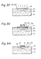
silicon nitride layer 36 and thepolycrystalline silicon layer 35 are selectively etched by a conventional photoetching process. Approximately half of the original thickness of thepolycrystalline silicon layer 35 is removed at the etched portions. - As illustrated in Fig. 3F, the remaining half-thickness etched portions of the
polycrystalline silicon layer 35 are thermally oxidized down to thesilicon dioxide layer 34 to form asilicon dioxide portion 37 which surrounds the polycrystalline silicon island 38 and serves as interdevice dielectric isolation. Then the polycrystalline silicon island 38 is single crystallized by irradiation of a light beam, such as a laser, or of a particle beam, such as an electron beam. Namely, the polycrystalline silicon is laser annealed or electron beam annealed to form a single crystallinesilicon island layer 39. For example, an argon gas continuous wave laser having an output of lOW, a scanning speed of 10 cm/sec, and a beam spot size of from 50 to 100 µm, may be irradiated in a 50% overlapping manner to change the polycrystalline silicon to a single crystalline silicon. - As illustrated in Fig. 3G, the
silicon nitride layer 36 is removed, then the surface portion of thesingle crystalline layer 39 of P type is thermally oxidized to form agate insulating layer 40 of silicon dioxide having a thickness of from 30 to 100 nm. Apolycrystalline silicon layer 41 is formed, as a gate electrode, on thegate insulating layer 40 and on the fieldsilicon oxide layer 37 by the pyrolysis process or the PVD process. Then, a photoresist layer is formed on thepolycrystalline silicon layer 41, is exposed, and is developed. The remainingphotoresist layer 42 having a width of 2.0 µm or less is located above the projecting portion of thesilicon wafer 31. - As illustrated in Fig. 3H, the
polycrystalline silicon layer 41 and thegate insulating layer 40 are selectively etched by a suitable etchant to form, under the remainingphotoresist layer 42, agate electrode 41 and a gate insulatinglayer portion 40. N type impurities, e.g., phosphorus, are introduced into the P type singlecrystalline silicon layer 39 by a thermal diffusion process or an ion-implantation process to form asource region 42 and adrain region 43. During the introduction of impurities, thegate electrode 41 and thegate insulating layer 40 serve as a mask. Thus it is possible to produce a short channel MIS transistor, with an N channel, comprising thegate electrode 41, thegate insulating layer 40, thesource region 42, thedrain region 43, and thechannel region 44 being a portion of the singlecrystalline silicon layer 39. - Instead of a N-channel MIS transistor, it is possible to produce a P channel MIS transistor.
Claims (9)
Applications Claiming Priority (2)
| Application Number | Priority Date | Filing Date | Title |
|---|---|---|---|
| JP62161/81 | 1981-04-24 | ||
| JP6216181A JPS57177559A (en) | 1981-04-24 | 1981-04-24 | Semiconductor device and manufacture thereof |
Publications (3)
| Publication Number | Publication Date |
|---|---|
| EP0063915A2 true EP0063915A2 (en) | 1982-11-03 |
| EP0063915A3 EP0063915A3 (en) | 1982-12-29 |
| EP0063915B1 EP0063915B1 (en) | 1985-11-27 |
Family
ID=13192109
Family Applications (1)
| Application Number | Title | Priority Date | Filing Date |
|---|---|---|---|
| EP19820302041 Expired EP0063915B1 (en) | 1981-04-24 | 1982-04-21 | A metal insulator semiconductor transistor |
Country Status (3)
| Country | Link |
|---|---|
| EP (1) | EP0063915B1 (en) |
| JP (1) | JPS57177559A (en) |
| DE (1) | DE3267657D1 (en) |
Cited By (7)
| Publication number | Priority date | Publication date | Assignee | Title |
|---|---|---|---|---|
| US4965872A (en) * | 1988-09-26 | 1990-10-23 | Vasudev Prahalad K | MOS-enhanced, self-aligned lateral bipolar transistor made of a semiconductor on an insulator |
| US5164805A (en) * | 1988-08-22 | 1992-11-17 | Massachusetts Institute Of Technology | Near-intrinsic thin-film SOI FETS |
| EP0621644A2 (en) * | 1993-04-23 | 1994-10-26 | International Business Machines Corporation | Semiconductor-on-insulator field-effect transistor |
| EP0709897A1 (en) * | 1992-12-24 | 1996-05-01 | OHMI, Tadahiro | Semiconductor device |
| EP0747940A2 (en) * | 1995-06-07 | 1996-12-11 | STMicroelectronics, Inc. | Fully-dielectric-isolated FET technology |
| EP0810652A2 (en) * | 1992-01-28 | 1997-12-03 | Canon Kabushiki Kaisha | Semiconductor device and manufacture method of same |
| EP1402573A1 (en) * | 2001-06-12 | 2004-03-31 | International Business Machines Corporation | Method and structure for buried circuits and devices |
Families Citing this family (1)
| Publication number | Priority date | Publication date | Assignee | Title |
|---|---|---|---|---|
| JPH08153880A (en) * | 1994-09-29 | 1996-06-11 | Toshiba Corp | Semiconductor device and fabrication thereof |
Citations (2)
| Publication number | Priority date | Publication date | Assignee | Title |
|---|---|---|---|---|
| US3470610A (en) * | 1967-08-18 | 1969-10-07 | Conductron Corp | Method of producing a control system |
| US4163984A (en) * | 1978-01-27 | 1979-08-07 | Raytheon Company | Field effect transistor |
-
1981
- 1981-04-24 JP JP6216181A patent/JPS57177559A/en active Pending
-
1982
- 1982-04-21 DE DE8282302041T patent/DE3267657D1/en not_active Expired
- 1982-04-21 EP EP19820302041 patent/EP0063915B1/en not_active Expired
Patent Citations (2)
| Publication number | Priority date | Publication date | Assignee | Title |
|---|---|---|---|---|
| US3470610A (en) * | 1967-08-18 | 1969-10-07 | Conductron Corp | Method of producing a control system |
| US4163984A (en) * | 1978-01-27 | 1979-08-07 | Raytheon Company | Field effect transistor |
Cited By (15)
| Publication number | Priority date | Publication date | Assignee | Title |
|---|---|---|---|---|
| US5164805A (en) * | 1988-08-22 | 1992-11-17 | Massachusetts Institute Of Technology | Near-intrinsic thin-film SOI FETS |
| US4965872A (en) * | 1988-09-26 | 1990-10-23 | Vasudev Prahalad K | MOS-enhanced, self-aligned lateral bipolar transistor made of a semiconductor on an insulator |
| EP0810652A2 (en) * | 1992-01-28 | 1997-12-03 | Canon Kabushiki Kaisha | Semiconductor device and manufacture method of same |
| US6096582A (en) * | 1992-01-28 | 2000-08-01 | Canon Kabushiki Kaisha | Method of making a semiconductor device |
| EP0810652A3 (en) * | 1992-01-28 | 1998-05-20 | Canon Kabushiki Kaisha | Semiconductor device and manufacture method of same |
| EP0709897A1 (en) * | 1992-12-24 | 1996-05-01 | OHMI, Tadahiro | Semiconductor device |
| EP0709897A4 (en) * | 1992-12-24 | 1997-05-28 | Tadahiro Ohmi | Semiconductor device |
| EP0621644A3 (en) * | 1993-04-23 | 1995-08-16 | Ibm | Semiconductor-on-insulator field-effect transistor. |
| EP0621644A2 (en) * | 1993-04-23 | 1994-10-26 | International Business Machines Corporation | Semiconductor-on-insulator field-effect transistor |
| US5981318A (en) * | 1995-02-28 | 1999-11-09 | Stmicroelectronics, Inc. | Fully-dielectric-isolated FET technology |
| US6291845B1 (en) | 1995-02-28 | 2001-09-18 | Stmicroelectronics, Inc. | Fully-dielectric-isolated FET technology |
| EP0747940A2 (en) * | 1995-06-07 | 1996-12-11 | STMicroelectronics, Inc. | Fully-dielectric-isolated FET technology |
| EP0747940A3 (en) * | 1995-06-07 | 1999-05-06 | STMicroelectronics, Inc. | Fully-dielectric-isolated FET technology |
| EP1402573A1 (en) * | 2001-06-12 | 2004-03-31 | International Business Machines Corporation | Method and structure for buried circuits and devices |
| EP1402573A4 (en) * | 2001-06-12 | 2010-09-15 | Ibm | Method and structure for buried circuits and devices |
Also Published As
| Publication number | Publication date |
|---|---|
| DE3267657D1 (en) | 1986-01-09 |
| EP0063915B1 (en) | 1985-11-27 |
| EP0063915A3 (en) | 1982-12-29 |
| JPS57177559A (en) | 1982-11-01 |
Similar Documents
| Publication | Publication Date | Title |
|---|---|---|
| US4149307A (en) | Process for fabricating insulated-gate field-effect transistors with self-aligned contacts | |
| US4954855A (en) | Thin film transistor formed on insulating substrate | |
| KR900007905B1 (en) | Semiconductor device | |
| US3475234A (en) | Method for making mis structures | |
| US5006913A (en) | Stacked type semiconductor device | |
| KR930001559B1 (en) | Manufacturing method of fet | |
| US5476802A (en) | Method for forming an insulated gate field effect transistor | |
| US4654958A (en) | Process for forming isolated silicon regions and field-effect devices on a silicon substrate | |
| US5158903A (en) | Method for producing a field-effect type semiconductor device | |
| US4597827A (en) | Method of making MIS field effect transistor having a lightly-doped region | |
| US4459739A (en) | Thin film transistors | |
| US5518941A (en) | Maskless method for formation of a field implant channel stop region | |
| US4119992A (en) | Integrated circuit structure and method for making same | |
| EP0063915B1 (en) | A metal insulator semiconductor transistor | |
| US4160683A (en) | Method of manufacturing field effect transistors of the MOS-type | |
| US5264721A (en) | Insulated-gate FET on an SOI-structure | |
| US4169746A (en) | Method for making silicon on sapphire transistor utilizing predeposition of leads | |
| KR100202048B1 (en) | Process for fabricating power-mos semiconductor device and device obtained therewith | |
| US5319231A (en) | Insulated gate semiconductor device having an elevated plateau like portion | |
| US4722912A (en) | Method of forming a semiconductor structure | |
| JP3380516B2 (en) | Semiconductor device and manufacturing method thereof | |
| EP0545484B1 (en) | Manufacturing process for insulated gate field effect transistors (igfet) with low short circuit density between gate and source and devices obtained thereby | |
| KR880001956B1 (en) | Method of producing semiconductor integrated circuit | |
| KR930011472B1 (en) | Manufacturing method of mos transistor | |
| JPH0620130B2 (en) | MIS transistor and manufacturing method thereof |
Legal Events
| Date | Code | Title | Description |
|---|---|---|---|
| PUAI | Public reference made under article 153(3) epc to a published international application that has entered the european phase |
Free format text: ORIGINAL CODE: 0009012 |
|
| PUAL | Search report despatched |
Free format text: ORIGINAL CODE: 0009013 |
|
| AK | Designated contracting states |
Designated state(s): DE FR GB NL |
|
| RHK1 | Main classification (correction) |
Ipc: H01L 29/78 |
|
| AK | Designated contracting states |
Designated state(s): DE FR GB NL |
|
| 17P | Request for examination filed |
Effective date: 19830307 |
|
| GRAA | (expected) grant |
Free format text: ORIGINAL CODE: 0009210 |
|
| AK | Designated contracting states |
Designated state(s): DE FR GB NL |
|
| REF | Corresponds to: |
Ref document number: 3267657 Country of ref document: DE Date of ref document: 19860109 |
|
| ET | Fr: translation filed | ||
| PLBE | No opposition filed within time limit |
Free format text: ORIGINAL CODE: 0009261 |
|
| STAA | Information on the status of an ep patent application or granted ep patent |
Free format text: STATUS: NO OPPOSITION FILED WITHIN TIME LIMIT |
|
| 26N | No opposition filed | ||
| PGFP | Annual fee paid to national office [announced via postgrant information from national office to epo] |
Ref country code: FR Payment date: 19890427 Year of fee payment: 8 |
|
| PGFP | Annual fee paid to national office [announced via postgrant information from national office to epo] |
Ref country code: NL Payment date: 19890430 Year of fee payment: 8 Ref country code: GB Payment date: 19890430 Year of fee payment: 8 |
|
| PGFP | Annual fee paid to national office [announced via postgrant information from national office to epo] |
Ref country code: DE Payment date: 19890621 Year of fee payment: 8 |
|
| PG25 | Lapsed in a contracting state [announced via postgrant information from national office to epo] |
Ref country code: GB Effective date: 19900421 |
|
| PG25 | Lapsed in a contracting state [announced via postgrant information from national office to epo] |
Ref country code: NL Effective date: 19901101 |
|
| NLV4 | Nl: lapsed or anulled due to non-payment of the annual fee | ||
| GBPC | Gb: european patent ceased through non-payment of renewal fee | ||
| PG25 | Lapsed in a contracting state [announced via postgrant information from national office to epo] |
Ref country code: FR Effective date: 19901228 |
|
| PG25 | Lapsed in a contracting state [announced via postgrant information from national office to epo] |
Ref country code: DE Effective date: 19910101 |
|
| REG | Reference to a national code |
Ref country code: FR Ref legal event code: ST |