EP0056064A1 - Switching unit - Google Patents
Switching unit Download PDFInfo
- Publication number
- EP0056064A1 EP0056064A1 EP81100098A EP81100098A EP0056064A1 EP 0056064 A1 EP0056064 A1 EP 0056064A1 EP 81100098 A EP81100098 A EP 81100098A EP 81100098 A EP81100098 A EP 81100098A EP 0056064 A1 EP0056064 A1 EP 0056064A1
- Authority
- EP
- European Patent Office
- Prior art keywords
- circuit unit
- unit according
- reading
- elements
- coupling elements
- Prior art date
- Legal status (The legal status is an assumption and is not a legal conclusion. Google has not performed a legal analysis and makes no representation as to the accuracy of the status listed.)
- Granted
Links
Images


Classifications
-
- G—PHYSICS
- G06—COMPUTING; CALCULATING OR COUNTING
- G06K—GRAPHICAL DATA READING; PRESENTATION OF DATA; RECORD CARRIERS; HANDLING RECORD CARRIERS
- G06K19/00—Record carriers for use with machines and with at least a part designed to carry digital markings
- G06K19/06—Record carriers for use with machines and with at least a part designed to carry digital markings characterised by the kind of the digital marking, e.g. shape, nature, code
- G06K19/067—Record carriers with conductive marks, printed circuits or semiconductor circuit elements, e.g. credit or identity cards also with resonating or responding marks without active components
- G06K19/07—Record carriers with conductive marks, printed circuits or semiconductor circuit elements, e.g. credit or identity cards also with resonating or responding marks without active components with integrated circuit chips
- G06K19/077—Constructional details, e.g. mounting of circuits in the carrier
- G06K19/07749—Constructional details, e.g. mounting of circuits in the carrier the record carrier being capable of non-contact communication, e.g. constructional details of the antenna of a non-contact smart card
- G06K19/07773—Antenna details
- G06K19/07788—Antenna details the antenna being of the capacitive type
-
- G—PHYSICS
- G06—COMPUTING; CALCULATING OR COUNTING
- G06K—GRAPHICAL DATA READING; PRESENTATION OF DATA; RECORD CARRIERS; HANDLING RECORD CARRIERS
- G06K19/00—Record carriers for use with machines and with at least a part designed to carry digital markings
- G06K19/06—Record carriers for use with machines and with at least a part designed to carry digital markings characterised by the kind of the digital marking, e.g. shape, nature, code
- G06K19/067—Record carriers with conductive marks, printed circuits or semiconductor circuit elements, e.g. credit or identity cards also with resonating or responding marks without active components
- G06K19/07—Record carriers with conductive marks, printed circuits or semiconductor circuit elements, e.g. credit or identity cards also with resonating or responding marks without active components with integrated circuit chips
- G06K19/0723—Record carriers with conductive marks, printed circuits or semiconductor circuit elements, e.g. credit or identity cards also with resonating or responding marks without active components with integrated circuit chips the record carrier comprising an arrangement for non-contact communication, e.g. wireless communication circuits on transponder cards, non-contact smart cards or RFIDs
- G06K19/0728—Record carriers with conductive marks, printed circuits or semiconductor circuit elements, e.g. credit or identity cards also with resonating or responding marks without active components with integrated circuit chips the record carrier comprising an arrangement for non-contact communication, e.g. wireless communication circuits on transponder cards, non-contact smart cards or RFIDs the arrangement being an optical or sound-based communication interface
-
- G—PHYSICS
- G06—COMPUTING; CALCULATING OR COUNTING
- G06K—GRAPHICAL DATA READING; PRESENTATION OF DATA; RECORD CARRIERS; HANDLING RECORD CARRIERS
- G06K19/00—Record carriers for use with machines and with at least a part designed to carry digital markings
- G06K19/06—Record carriers for use with machines and with at least a part designed to carry digital markings characterised by the kind of the digital marking, e.g. shape, nature, code
- G06K19/067—Record carriers with conductive marks, printed circuits or semiconductor circuit elements, e.g. credit or identity cards also with resonating or responding marks without active components
- G06K19/07—Record carriers with conductive marks, printed circuits or semiconductor circuit elements, e.g. credit or identity cards also with resonating or responding marks without active components with integrated circuit chips
- G06K19/077—Constructional details, e.g. mounting of circuits in the carrier
- G06K19/07749—Constructional details, e.g. mounting of circuits in the carrier the record carrier being capable of non-contact communication, e.g. constructional details of the antenna of a non-contact smart card
-
- G—PHYSICS
- G06—COMPUTING; CALCULATING OR COUNTING
- G06K—GRAPHICAL DATA READING; PRESENTATION OF DATA; RECORD CARRIERS; HANDLING RECORD CARRIERS
- G06K7/00—Methods or arrangements for sensing record carriers, e.g. for reading patterns
- G06K7/10—Methods or arrangements for sensing record carriers, e.g. for reading patterns by electromagnetic radiation, e.g. optical sensing; by corpuscular radiation
- G06K7/10009—Methods or arrangements for sensing record carriers, e.g. for reading patterns by electromagnetic radiation, e.g. optical sensing; by corpuscular radiation sensing by radiation using wavelengths larger than 0.1 mm, e.g. radio-waves or microwaves
- G06K7/10316—Methods or arrangements for sensing record carriers, e.g. for reading patterns by electromagnetic radiation, e.g. optical sensing; by corpuscular radiation sensing by radiation using wavelengths larger than 0.1 mm, e.g. radio-waves or microwaves using at least one antenna particularly designed for interrogating the wireless record carriers
- G06K7/10326—Methods or arrangements for sensing record carriers, e.g. for reading patterns by electromagnetic radiation, e.g. optical sensing; by corpuscular radiation sensing by radiation using wavelengths larger than 0.1 mm, e.g. radio-waves or microwaves using at least one antenna particularly designed for interrogating the wireless record carriers the antenna being of the very-near field type, e.g. capacitive
-
- G—PHYSICS
- G06—COMPUTING; CALCULATING OR COUNTING
- G06K—GRAPHICAL DATA READING; PRESENTATION OF DATA; RECORD CARRIERS; HANDLING RECORD CARRIERS
- G06K7/00—Methods or arrangements for sensing record carriers, e.g. for reading patterns
- G06K7/10—Methods or arrangements for sensing record carriers, e.g. for reading patterns by electromagnetic radiation, e.g. optical sensing; by corpuscular radiation
- G06K7/10544—Methods or arrangements for sensing record carriers, e.g. for reading patterns by electromagnetic radiation, e.g. optical sensing; by corpuscular radiation by scanning of the records by radiation in the optical part of the electromagnetic spectrum
- G06K7/10821—Methods or arrangements for sensing record carriers, e.g. for reading patterns by electromagnetic radiation, e.g. optical sensing; by corpuscular radiation by scanning of the records by radiation in the optical part of the electromagnetic spectrum further details of bar or optical code scanning devices
- G06K7/1097—Optical sensing of electronic memory record carriers, such as interrogation of RFIDs with an additional optical interface
-
- G—PHYSICS
- G07—CHECKING-DEVICES
- G07C—TIME OR ATTENDANCE REGISTERS; REGISTERING OR INDICATING THE WORKING OF MACHINES; GENERATING RANDOM NUMBERS; VOTING OR LOTTERY APPARATUS; ARRANGEMENTS, SYSTEMS OR APPARATUS FOR CHECKING NOT PROVIDED FOR ELSEWHERE
- G07C9/00—Individual registration on entry or exit
- G07C9/20—Individual registration on entry or exit involving the use of a pass
- G07C9/29—Individual registration on entry or exit involving the use of a pass the pass containing active electronic elements, e.g. smartcards
-
- G—PHYSICS
- G07—CHECKING-DEVICES
- G07F—COIN-FREED OR LIKE APPARATUS
- G07F7/00—Mechanisms actuated by objects other than coins to free or to actuate vending, hiring, coin or paper currency dispensing or refunding apparatus
- G07F7/08—Mechanisms actuated by objects other than coins to free or to actuate vending, hiring, coin or paper currency dispensing or refunding apparatus by coded identity card or credit card or other personal identification means
- G07F7/0866—Mechanisms actuated by objects other than coins to free or to actuate vending, hiring, coin or paper currency dispensing or refunding apparatus by coded identity card or credit card or other personal identification means by active credit-cards adapted therefor
Definitions
- the invention relates to a circuit unit which has a circuit integrated on a substrate and which, for its operation, has coupling elements for energy transmission, data output and, if appropriate, data input.
- Circuit units in the form of integrated circles are today mostly implemented on a single semiconductor chip (substrate). These semiconductor chips have metallized connection points at their edges, via which they can be connected to the connection points of the surrounding housing or directly to the surrounding circuit via suitable welding or soldering methods via wires.
- circuit units in identification cards creates difficulties because the cards are subject to mechanical stresses in use and, as a result, the galvanic connections between the circuit unit and the connection points on the card can be destroyed.
- the introduction of the circuit units in identification cards is also made more difficult due to the connecting lines, which are sensitive to mechanical stress.
- the object of the invention is therefore to propose an integrated circuit unit for the above-mentioned or similar applications, the coupling elements of which are designed in such a way that they are largely insensitive to mechanical loads.
- the object is achieved in that all coupling elements are arranged on the substrate receiving the integrated circuit.
- the substrate also has elements for data transformation and energy supply which are connected directly to the substrate.
- the circuit unit is such a compact unit, which in a simple manner, for. B. in an arbitrarily designed identification element, such as an identification card, coin, ring, etc., can be introduced and ensures extremely trouble-free operation due to the lack of connecting lines in use.
- the compact embodiment offers further possibilities for the miniaturization of such circuit units, which results in applications which previously closed circuit units were closed.
- integrated light converters such as photo elements
- the recording and also the output of data can also be done optically, for example using a liquid crystal display for data output and corresponding light-sensitive elements such as photodiodes for data recording.
- the data can also be entered capacitively or
- the transmit and receive electrodes required for this are vapor-deposited directly onto the substrate in the form of conductive coatings.
- the coupling elements are in direct contact with the substrate without any connecting lines.
- FIG. 1a and 1b show a circuit unit 15 according to the invention in a schematic, greatly enlarged simple embodiment.
- This can be, for example, a circuit unit which is supplied with energy via photoelectric converters and which also has elements which can be used to output certain information during operation.
- Installed in an identification card the circuit unit can be used, for example, to store a code word, so that the card can be used as an electronic key for access control or the like.
- an integrated circuit 2 produced in a known manner is located on a silicon wafer 1 (substrate).
- the integrated circuit Circuit 2 covers only a small part of the chip 1.
- photosensitive semiconductors for example photo elements 3 are integrated, which deliver the energy required for the operation of the integrated circuit in a known manner, depending on the striking radiation power.
- the elements are connected to one another and to the integrated circuit with the aid of guide bars which, as is customary in the production of integrated circuits, are vapor-deposited onto the plate 1.
- the data are output via so-called liquid crystal elements 4, which are often used today as display elements.
- the liquid crystal element consists of a liquid crystal layer 5 which is enclosed in a frame 8 between two transparent electrodes 6, 7.
- the frame 8 is adapted to the size of the silicon wafer 1.
- liquid crystal layers have the property of changing their light transmission with extremely low energy consumption as soon as an electric field is applied to the conductive documents 6, 7 attached to both sides of the layer.
- the illuminated liquid crystal layer appears milky to a viewer, while in the excited state it becomes clear and transparent, the underlying surface, in FIG. 1b, a darkly colored layer 10 becoming visible.
- the frame 8 carrying the liquid crystal is firmly connected to the silicon wafer 1, for example using a suitable adhesive, the electrodes 6, 7 being in the through Contacting method are combined with the corresponding connections of the integrated circuit 2.
- the frame 8 is translucent in the spectral range relevant for the photo elements 3, so that their function is not impaired by the cover of the photo elements 3.
- the arrangement of the data output element 4 and the energy supply element 3 has the advantage, especially when using liquid crystal elements for data output, that when the circuit unit is illuminated over a large area, both the photo elements are activated and the liquid crystal display is illuminated.
- the operation of the circuit unit is therefore possible without complex positioning problems and without great effort (only one lighting unit).
- the elements for the energy supply and for the data output do not necessarily have to be arranged on only one side of the silicon wafer.
- FIG. 2a shows a circuit unit 15 built into an identification card 16.
- the circuit unit in its simplest embodiment has the task of outputting only defined information, for example in the form of an identification number, during a control process. The number is stored in a corresponding, non-volatile memory within the circuit unit when it is manufactured using known methods.
- FIG. 2b shows, the identification card is checked when checking the identification number. guided under a device 17, which has, inter alia, a light source 18 for irradiating the circuit unit 15. Due to the radiation, the photo elements 3 deliver the energy necessary for the operation of the unit. As soon as the circuit is ready for operation, the information stored in FIG. 1b.
- liquid crystal element 4 which is also irradiated by the illumination source, in the form of light / dark modulations.
- the liquid crystal element is imaged on a photodiode 23 with the aid of an optical system consisting of an aperture 20 and two lenses 21, 22.
- the identification card within the control device can be adjusted using appropriate mechanical positioning aids (not shown).
- the circuit unit described in FIGS. 1a, 1b is only able to output a fixedly specified, non-changeable information that is typical for each identification card during the control process.
- a suitable embodiment consists, for example, of feeding in the data to be supplied externally via the photo elements used to power the circuit unit.
- the circuit unit can have the structure shown in Fig. 1a, 1b purely on the outside.
- the light used to illuminate the photo elements is composed of a DC component and an AC component containing the information, so that the photo elements irradiated with light modulated in this way deliver correspondingly modulated electrical signals.
- the alternating component is decoupled via known electrical filters and, if necessary after appropriate amplification, fed to the subsequent electronic circuits as information.
- FIG. 3 Another possibility of providing the circuit unit externally with data is shown in FIG. 3.
- the surface of the circuit unit has an area 26 which is insulated from the environment - indicated by double hatching in the figure - in which an additional photodiode is integrated in the silicon substrate.
- the photodiode converts the light modulated according to the information to be entered into electrical signals.
- a separation of the luminous fluxes for the energy supply and the data input is useful in the latter embodiment. For example, this can be done with the help Optical imaging systems that illuminate the areas 3, 26 separately.
- the area 26 for the data input is illuminated with a spectrum which lacks the IR component, while the area 3 for the energy supply is illuminated exclusively with IR light.
- the supply of the energy area with IR light uses the property of silicon photo elements to be particularly sensitive in this area, so that a good efficiency can be achieved even with photo elements with small dimensions.
- the area for data entry can of course also be illuminated with IR light or with light from another spectral range.
- the light currents at the receiving end are separated by appropriate detectors that are sensitive to the respective light range.
- optical filters which are each only permeable to the light in question.
- 4a-4d the latter is schematically outlined.
- 4a and 4b show the spectra for the illumination of areas 3 (energy supply) and 26 (data input).
- 4c and 4d show the attenuation curves of the filters to be used for areas 3 and 26.
- the frequency separation in the light fluxes has the advantage over the separation of the fluxes of light through optical systems the advantage that the identification card in the field of S c h al- processing unit can be irradiated relative to the size of the circuit unit over a large area. An adjustment of the lighting cone is unnecessary.
- the data output by means of liquid crystal elements was technikstelligt loading j advantageous because of the very low energy requirement can be used.
- the embodiments require a hybrid construction of the circuit unit. If the elements required for data output are also integrated into the silicon plate, the circuit unit is monolithically constructed. In principle, this can be achieved by using light-emitting diodes which can be integrated directly into the substrate for the data output, although the high current consumption of these elements can be disadvantageous for special fields of application.
- FIG. 5 An advantageous embodiment is shown in FIG. 5.
- the data is capacitively coupled in or out.
- photo elements 3 are provided for the energy supply, which are integrated directly into the silicon wafer in addition to the integrated circuit 2.
- FIG. 6 shows the operation of an identification card equipped with the latter switching circuit in a control device.
- the identification card in the area of the circuit unit a counter electrode 33 is placed, which can be considerably larger than the circuit itself. Due to the use of only one counter electrode, which can also be relatively large compared to the identification card, there are no problems with the adjustment of the card within the control device.
- the electrode which is made of translucent material, is also provided with a translucent but conductive coating 34, so that the light from the illumination sources 35 can reach the photo elements of the circuit unhindered.
- the control device communicates with the circuit unit of the identification card using the so-called time-division multiplex method. Data input and output are carried out serially within defined time windows.
- the window for data acquisition is first generated and the corresponding receiving electrode (see FIG. 5, for example, electrode 30) is set to work.
- the electrode 33 of the control device acts as a transmitter in this phase.
- the integrated circuit generates a sequence of equidistant "raster points" within the recording window.
- the logic of the integrated circuit interprets this, for example, as logic 1, otherwise, if there is no pulse between 2 raster points, as logic 0
- the potentials on the conductive coating 30 gels Data pulses are defined against the coating 31, which is vapor-deposited on the underside of the silicon wafer and held capacitively at reference potential by the grounded base plate 40 of the control device.
- the data is output like the data is recorded according to the principle described above, as soon as the "Data output" window has been generated again after a defined time. During this time, the applied electrode 33, coupled to the conductive coating 30, works as a receiver.
- the data input and output times can be defined according to known methods by corresponding control information that the control device transmits to the circuit unit.
Abstract
Beschrieben wird eine Schaltungseinheit, bestehend aus einem auf einem Substrat als Träger angeordneten integrierten Schaltkreis und Kopplungselementen zur Energieübertragung, Datenausgabe und gegebenenfalls Dateneingabe. Dabei sind alle Kopplungselemente auf dem den integrierten Schaltkreis aufnehmenden Substrat angeordnet. Die Schaltungseinheiten können vorteilhaft in Ausweiskarten eingebettet werden.A circuit unit is described, consisting of an integrated circuit arranged on a substrate as a carrier and coupling elements for energy transmission, data output and, if appropriate, data input. All coupling elements are arranged on the substrate receiving the integrated circuit. The circuit units can advantageously be embedded in identity cards.
Description
Die Erfindung betrifft eine Schaltungseinheit, die einen auf einem Substrat integrierten Schaltkreis aufweist und die zu ihrem Betrieb über Koppelungselemente zur Energieübertragung, Datenausgabe und gegebenenfalls Dateneingabe verfügt.The invention relates to a circuit unit which has a circuit integrated on a substrate and which, for its operation, has coupling elements for energy transmission, data output and, if appropriate, data input.
Schaltungseinheiten in Form integrierter Kreise werden heute in der Mehrzahl auf einem einzigen Halbleiterchip (Substrat) realisiert. Diese Halbleiterchips besitzen an ihren Rändern metallisierte Anschlußpunkte, über die sie über geeignete Schweiß- oder Lötverfahren über Drähte mit den Anschlußstellen des sie umgebenden Gehäuses oder direkt mit der umgebenden Schaltung verbunden werden können.Circuit units in the form of integrated circles are today mostly implemented on a single semiconductor chip (substrate). These semiconductor chips have metallized connection points at their edges, via which they can be connected to the connection points of the surrounding housing or directly to the surrounding circuit via suitable welding or soldering methods via wires.
Es gibt Anwendungen, in denen die galvanische Verbindung des Halbleiterchips mit seiner Umgebung unerwünscht ist. So ist z. B. vorgeschlagen worden (DE-OS 26 59 573), Identifikationskarten mit Halbleiterchips auszurüsten, um hierdurch ihre Nachahmungssicherheit zu verbessern, zugleich eine Vielzahl von Informationen in der Identifikationskarte zu speichern und gegebenenfalls diese Informationen im Zusammenwirken mit Sendern und Empfängern in einem kontrollierenden Gerät zu verändern.There are applications in which the galvanic connection of the semiconductor chip to its surroundings is undesirable. So z. B. has been proposed (DE-OS 26 59 573) to equip identification cards with semiconductor chips in order to thereby improve their counterfeiting security, at the same time storing a large amount of information in the identification card and, if appropriate, this information in cooperation with transmitters and receivers in a controlling device change.
Die Einbringung von Schaltungseinheiten in Identifikationskarten macht Schwierigkeiten, weil die Karten im Gebrauch mechanischen Beanspruchungen unterliegen und hierdurch besonders die galvanischen Verbindungen zwischen der Schaltungseinheit und den auf der Karte befindlichen Anschlußpunkten zerstört werden können. Auch die Einbringung der Schaltungseinheiten in Identifikationskarten ist aufgrund der gegen mechanische Beanspruchungen empfindlichen Anschlußleitungen erschwert.The introduction of circuit units in identification cards creates difficulties because the cards are subject to mechanical stresses in use and, as a result, the galvanic connections between the circuit unit and the connection points on the card can be destroyed. The introduction of the circuit units in identification cards is also made more difficult due to the connecting lines, which are sensitive to mechanical stress.
Es wurde daher bereits vorgeschlagen (DE-OS 19 45 777), die für die Datenaufnahme und Datenausgabe zuständigen Kopplungselemente ohne Anschlußleitungen direkt auf dem Halbleiterchip anzuordnen, die in einem sogenannten "Identifikaten", beispielsweise zur Identifizierung von Personen, untergebracht sind. Die Daten werden dabei über Lichtleiterbündel übertragen, die kongruent zu den Kopplungselementen auf die Schaltungseinheit aufgesetzt werden müssen. Die Energie wird kapazitiv über entsprechende metallische Flächen übertragen, die auf der Außenfläche des Identifikanten aufgebracht sind. Die Flächen sind durch Anschlußleitungen mit dem Halbleiterchip verbunden, womit sich die schon oben genannten Schwierigkeiten ergeben.It has therefore already been proposed (DE-OS 19 45 777) to arrange the coupling elements responsible for data acquisition and data output without connecting lines directly on the semiconductor chip, which are accommodated in a so-called "identifiers", for example for identifying people. The data are transmitted via fiber optic bundles, which must be placed on the circuit unit in a congruent manner with the coupling elements. The energy is transferred capacitively via corresponding metallic surfaces that are applied to the outer surface of the identifier. The surfaces are connected to the semiconductor chip by connecting lines, which results in the difficulties already mentioned.
Die Aufgabe der Erfindung besteht deshalb darin, eine integrierte Schaltungseinheit für oben genannte oder ähnliche Anwendungen vorzuschlagen, deren Kopplungselemente so ausgebildet sind, daß sie gegen mechanische Beanspruchungen weitgehend unempfindlich sind.The object of the invention is therefore to propose an integrated circuit unit for the above-mentioned or similar applications, the coupling elements of which are designed in such a way that they are largely insensitive to mechanical loads.
Die Aufgabe wird erfindungsgemäß dadurch gelöst, daß alle Kopplungselemente auf dem den integrierten Schaltkreis aufnehmenden Substrat angeordnet sind.The object is achieved in that all coupling elements are arranged on the substrate receiving the integrated circuit.
Das Substrat weist also außer dem integrierten Schaltkreis auch Elemente zur Datentransformation und Energieversorgung auf, die direkt mit dem Substrat verbunden sind. Die Schaltungseinheit ist so eine kompakte Einheit, die in einfacher Weise, z. B. in ein beliebig gestaltetes IdentifikationsElement, wie eine Identifikations-Karte, Münze, Ring etc., eingebracht werden kann und aufgrund nicht vorhandener Anschlußleitungen im Gebrauch einen äußerst störungsfreien Betrieb gewährleistet. Schließlich bietet die kompakte Ausführungsform weitere Möglichkeiten zur Miniaturisierung derartiger Schaltungseinheiten, wodurch sich Anwendungsfälle ergeben, die bisher bekannten Schaltungseinheiten verschlossen waren.In addition to the integrated circuit, the substrate also has elements for data transformation and energy supply which are connected directly to the substrate. The circuit unit is such a compact unit, which in a simple manner, for. B. in an arbitrarily designed identification element, such as an identification card, coin, ring, etc., can be introduced and ensures extremely trouble-free operation due to the lack of connecting lines in use. Finally, the compact embodiment offers further possibilities for the miniaturization of such circuit units, which results in applications which previously closed circuit units were closed.
Zur Realisierung der Kopplungselemente im Sinne der Erfindung bieten sich eine Vielzahl von Möglichkeiten. So können beispielsweise zur Energieübertragung auf dem Substrat integrierte Lichtwandler, wie Fotoelemente, vorgesehen werden, die bei Lichteinfall den für den Schaltkreis notwendigen Strom liefern. Die Aufnahme und auch die Ausgabe von Daten kann ebenfalls auf optischem Weg erfolgen, wobei beispielsweise für die Datenausgabe eine Flüssigkristallanzeige verwendet wird und für die Datenaufnahme entsprechende lichtempfindliche Elemente, wie Fotodioden. Die Daten können auch kapazitiv eingegeben bzw.There are a multitude of possibilities for realizing the coupling elements in the sense of the invention. For example, integrated light converters, such as photo elements, can be provided for energy transmission on the substrate, which supply the current required for the circuit when light falls. The recording and also the output of data can also be done optically, for example using a liquid crystal display for data output and corresponding light-sensitive elements such as photodiodes for data recording. The data can also be entered capacitively or
ausgegeben werden. Die dazu notwendigen Sende- und Empfangselektroden werden in Form leitender Beläge direkt auf das Substrat aufgedampft.be issued. The transmit and receive electrodes required for this are vapor-deposited directly onto the substrate in the form of conductive coatings.
Entscheidend ist für alle Ausführungsformen, daß die Kopplungselemente ohne jegliche Anschlußleitungen in direktem Kontakt mit dem Substrat stehen.It is crucial for all embodiments that the coupling elements are in direct contact with the substrate without any connecting lines.
Weitere Vorteile und Weiterbildungen der Erfindung sind Gegenstand von Unteransprüchen. Nachfolgend werden Ausführungsbeispiele der Erfindung anhand der beigefügten Zeichnungen näher beschrieben. Darin zeigen:
- Fig. 1a, 1b eine optisch betriebene Schaltungseinheit in der Draufsicht und im Schnitt,
- Fig. 2a die Schaltungseinheit aus Fig. 1, eingebaut in eine Identifikationskarte,
- Fig. 2b die Identifikationskarte aus Fig. 2a in einem Kontrollgerät,
- Fig. 3 eine optisch betriebene Schaltungseinheit mit der Möglichkeit der Dateneingabe,
- Fig. 4a, 4b die Lichtspektren der Beleuchtungsquellen für Energieversorgung und Dateneingabe für die Schaltungseinheit aus Fig. 3,
- Fig. 4c, 4d die Dämpfungsverläufe der Filter zur Abdeckung des Dateneingabebereichs und des Energieversorgungsbereichs,
- Fig. 5 eine kapazitiv betriebene Schaltungseinheit und
- Fig. 6 die Schaltungseinheit aus Fig. 5 in einem Kontrollgerät.
- 1a, 1b an optically operated circuit unit in plan view and in section,
- 2a, the circuit unit from FIG. 1, installed in an identification card,
- 2b the identification card from Fig. 2a in a control device,
- 3 shows an optically operated circuit unit with the possibility of data input,
- 4a, 4b the light spectra of the illumination sources for energy supply and data input for the circuit unit from FIG. 3,
- 4c, 4d the attenuation curves of the filters to cover the data input area and the energy supply area,
- Fig. 5 is a capacitively operated circuit unit and
- FIG. 6 shows the circuit unit from FIG. 5 in a control device.
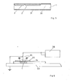
Fig. 1a und 1b zeigen eine Schaltungseinheit 15 gemäß der Erfindung in einer schematischen, stark vergrößerten einfachen Ausführungsform. Dies kann beispielsweise eine Schaltungseinheit sein, die über lichtelektrische Wandler mit Energie versorgt wird und die außerdem Elemente besitzt, mit deren Hilfe während des Betriebs das Ausgeben bestimmter Informationen möglich ist. Eingebaut in eine Identifikationskarte läßt sich die Schaltungseinheit beispielsweise zur Speicherung eines Codewortes nutzen, so daß die Karte als elektronischer Schlüssel zur Zugangskontrolle oder dergl. genutzt werden kann.1a and 1b show a
Wie aus der Darstellung in der Fig. 1b hervorgeht, befindet sich auf einem Siliziumplättchen 1 (Substrat) eine in bekannter Weise hergestellte integrierte Schaltung 2. Die integrierte Schaltung 2 bedeckt nur einen geringen Teil des Plättchens 1. In die verbleibende Fläche sind lichtempfindliche Halbleiter, beispielsweise Fotoelemente 3, integriert, die in bekannter Weise abhängig von der auffallenden Strahlungsleistung die für den Betrieb der integrierten Schaltung notwendige Energie liefern. Verbunden werden die Elemente untereinander und mit der integrierten Schaltung mit Hilfe von Leitstegen, die, wie bei der Herstellung von integrierten Schaltkreisen üblich, auf das Plättchen 1 aufgedampft werden.As can be seen from the illustration in FIG. 1b, an integrated
Die Daten werden über sogenannte Flüssigkristallelemente 4, die heute vielfach als Anzeigeelemente Verwendung finden, ausgegeben. Das Flüssigkristallelement besteht aus einer Flüssigkristallschicht 5, die zwischen zwei lichtdurchlässigen Elektroden 6, 7 in einem Rahmen 8 eingeschlossen ist. Der Rahmen 8 ist der Größe des Siliziumplättchens 1 angepaßt.The data are output via so-called liquid crystal elements 4, which are often used today as display elements. The liquid crystal element consists of a
Wie bekannt, haben Flüssigkristallschichten die Eigenschaft, bei äußerst geringem Energieverbrauch ihre Lichtdurchlässigkeit zu ändern, sobald man an die beidseitig der Schicht angebrachten leitenden Belege 6, 7 ein elektrisches Feld anlegt. So erscheint die beleuchtete Flüssigkristallschicht einem Betrachter einmal milchig trüb, während sie im angeregten Zustand klar durchsichtig wird, wobei der jeweils vorhandene Untergrund, in der Fig. 1b eine dunkel gefärbte Schicht 10, sichtbar wird. Zur Fertigstellung der Schaltungseinheit wird der den Flüssigkristall tragende Rahmen 8 beispielsweise mit einem geeigneten Kleber fest mit dem Silizium- plättchen 1 verbunden, wobei die Elektroden 6, 7 im Durchkontaktierverfahren mit den entsprechenden Anschlüssen der integrierten Schaltung 2 zusammengefügt werden.-Der Rahmen 8 ist in dem für die Fotoelemente 3 relevanten Spektralbereich lichtdurchlässig, so daß durch die Abdeckung der Fotoelemente 3 deren Funktion nicht beeinträchtigt ist. Die Anordnung des Datenausgabeelementes 4 und des Energieversorgungselementes 3 hat vor allem bei der Verwendung von Flüssigkristallelementen zur Datenausgabe den Vorteil, daß bei großflächiger Anstrahlung der Schaltungseinheit sowohl die Fotoelemente aktiviert als auch die Flüssigkristallanzeige beleuchtet wird. Der Betrieb der Schaltungseinheit ist dadurch ohne aufwendige Positionierprobleme und ohne großen Aufwand (nur eine Beleuchtungseinheit) möglich.As is known, liquid crystal layers have the property of changing their light transmission with extremely low energy consumption as soon as an electric field is applied to the
Die Elemente für die Energieversorgung und für die Datenausgabe müssen allerdings nicht zwingend nur auf einer Seite des Siliziumplättchens angeordnet werden.However, the elements for the energy supply and for the data output do not necessarily have to be arranged on only one side of the silicon wafer.
Fig.2a zeigt eine Schaltungseinheit 15, eingebaut in eine Identifikationskarte 16. Wie oben schon erwähnt, hat die Schaltungseinheit in ihrer einfachsten Ausführungsform die Aufgabe, während eines Kontrollvorgangs lediglich eine definierte Information, beispielsweise in Form einer Identifikations-Nr., auszugeben. Die Nummer wird in einem entsprechenden, nicht flüchtigen Speicher innerhalb der Schaltungseinheit bei dessen Herstellung nach bekannten Methoden gespeichert. Wie Fig. 2b zeigt, wird die Identifikationskarte bei der Prüfung der Identifikations-Nr. unter eine Vorrichtung 17 geführt, die unter anderem eine Lichtquelle 18 zur Bestrahlung der Schaltungseinheit 15 aufweist. Aufgrund der Strahlung liefern die Fotoelemente 3 die für den Betrieb der Einheit notwendige Energie. Sobald die Schaltung betriebsbereit ist, werden die gespeicherten Informationen über das in der Fig. 1b. gezeigte Flüssigkristallelement 4, das ebenfalls von der Beleuchtungsquelle bestrahlt wird, in Form von Hell-/Dunkel-Modulationen ausgegeben. Zur Auswertung der Hell-/Dunkel-Modulationen wird das Flüssigkristallelement mit Hilfe eines optischen Systems, bestehend aus einer Blende 20 und zwei Linsen 21, 22, auf einer Fotodiode 23 abgebildet. Die Justierung der Identifikationskarte innerhalb des Kontrollgerätes kann mit Hilfe entsprechender mechanischer Positionierhilfen (nicht dargestellt) durchgeführt werden.2a shows a
Die in den Fig. 1a, 1b beschriebene Schaltungseinheit ist lediglich in der Lage, eine fest vorgegebene, nicht veränderbare und für jede Identifikationskarte typische Information während des Kontrollvorgangs auszugeben. Für eine Reihe von Anwendungsfällen kann es jedoch wünschenswert sein, der Schaltungseinheit auch extern Daten zuzuführen, die in der integrierten Schaltung unter Umständen mit dort gespeicherten Daten verknüpft zu einer Ausgangsinformation verarbeitet werden, oder aber die in der integrierten Schaltung Speicherzustände ändern, die deren künftiges Verhalten beeinflussen. Eine auch für diese Aufgabe geeignete Ausführungsform besteht beispielsweise darin, die extern zuzuführenden Daten über die zur Stromversorgung der Schaltungseinheit verwendeten Fotoelemente einzuspeisen. Die Schaltungseinheit kann dabei rein äußerlich den in Fig. 1a, 1b gezeigten Aufbau haben. Bei dieser Ausführungsform setzt sich das zur Beleuchtung der Fotoelemente verwendete Licht aus einem Gleichanteil und einem die Information enthaltenden Wechselanteil zusammen, so daß die mit derart moduliertem Licht bestrahlten Fotoelemente entsprechend modulierte elektrische Signale liefern. Innerhalb der integrierten Schaltung wird der Wechselanteil über bekannte elektrische Filter ausgekoppelt und als Information gegebenenfalls nach entsprechender Verstärkung den nachfolgenden elektronischen Schaltungen zugeführt.The circuit unit described in FIGS. 1a, 1b is only able to output a fixedly specified, non-changeable information that is typical for each identification card during the control process. For a number of applications, however, it may be desirable to also externally supply the circuit unit with data which, under certain circumstances, may be processed in the integrated circuit with data stored there to produce output information, or which may change storage states in the integrated circuit which change their future behavior influence. One for this task too A suitable embodiment consists, for example, of feeding in the data to be supplied externally via the photo elements used to power the circuit unit. The circuit unit can have the structure shown in Fig. 1a, 1b purely on the outside. In this embodiment, the light used to illuminate the photo elements is composed of a DC component and an AC component containing the information, so that the photo elements irradiated with light modulated in this way deliver correspondingly modulated electrical signals. Within the integrated circuit, the alternating component is decoupled via known electrical filters and, if necessary after appropriate amplification, fed to the subsequent electronic circuits as information.
Eine andere Möglichkeit, die Schaltungseinheit extern mit Daten zu vorsorgen, ist in der Fig. 3 gezeigt. Die Oberfläche der Schaltungseinheit weist in diesem Fall ein gegenüber der Umgebung isolierten Bereich 26 auf - in der Fig. doppeltschraffiert angedeutet -, in dem in das Siliziumsubstrat eine zusätzliche Fotodiode integriert ist. Die Fotodiode wandelt das entsprechend der einzugebenden Information modulierte Licht in elektrische Signale um.Another possibility of providing the circuit unit externally with data is shown in FIG. 3. In this case, the surface of the circuit unit has an
Um eine Vereinfachung im Aufbau der integrierten Schaltung zu erreichen, ist bei der letztgenannten Ausführungsform eine Trennung der Lichtströme für die Energieversorgung und die Dateneingabe sinnvoll. Dies kann beispielsweise mit Hilfe optischer Abbildungssysteme geschehen, die die Bereiche 3, 26 getrennt beleuchten.To achieve a simplification in the structure of the integrated circuit, a separation of the luminous fluxes for the energy supply and the data input is useful in the latter embodiment. For example, this can be done with the help Optical imaging systems that illuminate the
Eine technisch einfacher zu realisierende Möglichkeit besteht darin, die Lichtströme frequenzmäßig zu trennen. Aus der Vielzahl der Möglichkeiten, die Lichtströme frequenzmäßig zu trennen, sei nachfolgend eine Ausführungsform genannt. Dabei wird der Bereich 26 für die Dateneingabe mit einem Spektrum beleuchtet, dem der IR-Anteil fehlt, während der Bereich 3 für die Energieversorgung ausschließlich mit IR-Licht beleuchtet wird. Die Versorgung des Energiebereichs mit IR-Licht nutzt die Eigenschaft von Siliziumfotoelementen gerade in diesem Bereich besonders empfindlich zu sein, so daß auch bei Fotoelementen mit kleinen Abmaßen ein guter Wirkungsgrad erzielt werden kann. Grundsätzlich kann natürlich der Bereich für die Dateneingabe umgekehrt auch mit IR-Licht oder mit Licht eines anderen Spektralbereichs beleuchtet werden. Die empfangsseitige Trennung der Lichtströme erfolgt durch entsprechende, für den jeweiligen Lichtbereich empfindliche Detektoren. Bei Verwendung physikalisch gleichwertiger Detektoren werden die Bereiche 3, 26 durch optische Filter abgedeckt, die jeweils nur für das infrage kommende Licht durchlässig sind. In den Fig. 4a - 4d ist der letztgenannte Sachverhalt schematisch skizziert. Die Fig. 4a und 4b zeigen die Spektren für die Beleuchtung der Bereiche 3 (Energieversorgung) und 26 (Dateneingabe). In den Fig. 4c und 4d sind die Dämpfungsverläufe der für die Bereiche 3 und 26 zu verwendenden Filter gezeigt.A technically easier to implement is to separate the luminous flux in terms of frequency. One embodiment is mentioned below from the large number of possibilities for frequency-separating the luminous fluxes. The
Die frequenzmäßige Trennung der Lichtströme hat gegenüber der Trennung der Lichtströme durch optische Systeme den Vorteil, daß die Identifikationskarte im Bereich der Schal- tungseinheit relativ zur Größe der Schaltungseinheit großflächig bestrahlt werden kann. Eine Justierung der Beleuchtungskegel erübrigt sich damit.The frequency separation in the light fluxes has the advantage over the separation of the fluxes of light through optical systems the advantage that the identification card in the field of S c h al- processing unit can be irradiated relative to the size of the circuit unit over a large area. An adjustment of the lighting cone is unnecessary.
In den bisher genannten Ausführungsbeispielen wurde die Datenausgabe mit Hilfe von Flüssigkristallelementen be- j werkstelligt, die aufgrund des sehr geringen Energiebedarfs vorteilhaft einsetzbar sind. Die Ausführungsformen erfordern jedoch aufgrund der Verknüpfung unterschiedlicher Technologien einen hybriden Aufbau der Schaltungseinheit. Werden auch die zur Datenausgabe notwendigen Elemente in das Silizium-Plättchen integriert, erhält man einen monolitischen Aufbau der Schaltungseinheit. Dies kann grundsätzlich dadurch erreicht werden, daß man für die Datenausgabe direkt in das Substrat integrierbare lichtemittierende Dioden verwendet, wobei allerdings der hohe Stromverbrauch dieser Elemente für spezielle Anwendungsbereiche nachteilig sein kann.In the previously mentioned embodiments, the data output by means of liquid crystal elements was werkstelligt loading j advantageous because of the very low energy requirement can be used. However, due to the combination of different technologies, the embodiments require a hybrid construction of the circuit unit. If the elements required for data output are also integrated into the silicon plate, the circuit unit is monolithically constructed. In principle, this can be achieved by using light-emitting diodes which can be integrated directly into the substrate for the data output, although the high current consumption of these elements can be disadvantageous for special fields of application.
Eine vorteilhaftere Ausführungsform ist in der Fig. 5 gezeigt. Bei dieser Schaltungseinheit werden die Daten kapazitiv ein- bzw. auch ausgekoppelt. Dazu befinden sich auf dem Silizium- plättchen 1 aufgedampfte leitende Beläge 30, 31, die über ebenfalls aufgedampfte Leitstege (in der Fig. nicht dargestellt) mit der integrierten Schaltung 2 verbunden sind. Für die Energieversorgung sind wieder Fotoelemente 3 vorgesehen, die neben der integrierten Schaltung 2 direkt in das Silizium- plättchen integriert sind.An advantageous embodiment is shown in FIG. 5. With this circuit unit, the data is capacitively coupled in or out. For this purpose, there are vapor-deposited
Fig. 6 zeigt den Betrieb einer mit dem letztgenannten Schalkreis ausgestatteten Identifikationskarte in einem Kontrollgerät. Um die Daten eingeben bzw. aufnehmen zu können, wird auf die Identifikationskarte im Bereich der Schaltungseinheit eine Gegenelektrode 33 aufgesetzt, die erheblich größer sein kann als der Schaltkreis selbst. Aufgrund der Verwendung nur einer Gegenelektrode, die zudem gegenüber der Identifikationskarte relativ großflächig sein kann, ergeben sich hinsichtlich der Justierung der Karte innerhalb des Kontrollgerätes keine Probleme. Die aus lichtdurchlässigem Material bestehende Elektrode ist mit einer ebenfalls lichtdurchlässigen, jedoch leitenden Beschichtung 34 versehen, so daß das Licht der Beleuchtungsquellen 35 ungehindert auf die Fotoelemente des Schaltkreises gelangen kann. Die Kommunikation des Kontrollgeräts mit der Schaltungseinheit der Identifikationskarte erfolgt nach dem sogenannten Zeitmultiplex-Verfahren. Dabei werden Datenein- und ausgabe innerhalb definierter Zeitfenster seriell vorgenommen. Nach der Inbetriebnahme des Schaltkreises, d. h. nach Ablauf einer definierten Zeitspanne nach Beleuchtung der Fotoelemente, wird zunächst das Fenster für die Datenaufnahme erzeugt und die entsprechende Empfangselektrode (s. Fig. 5 beispielsweise die Elektrode 30) in Arbeitsbereitschaft gesetzt. Die Elektrode 33 des Kontrollgerätes wirkt in dieser Phase als Sender. Innerhalb des Aufnahmefenster erzeugt die integrierte Schaltung eine Folge äquidistanter "Rasterpunkte". Erscheint innerhalb zweier Rasterpunkte ein durch eine Datensende- und empfangseinheit 36 erzeugter und an die aufgelegte Elektrode geführter Spannungsimpuls, so interpretiert die Logik des integrierten Schaltkreises das beispielsweise als logisch 1, im andern Fall, wenn also zwischen 2 Rasterpunkten kein Impuls erscheint, als logisch 0. Die Potentiale der auf den leitenden Belag 30 gele führten Datenimpulse sind dabei gegen den auf der Unterseite des Siliziumplättchens aufgedampften und durch die geerdete Grundplatte 40 des Kontrollgerätes kapazitiv auf Bezugspotential gehaltenen Belag 31 definiert.6 shows the operation of an identification card equipped with the latter switching circuit in a control device. In order to be able to enter or record the data, the identification card in the area of the circuit unit a
Die Ausgabe der Daten erfolgt wie die Aufnahme der Daten nach dem oben geschilderten Prinzip, sobald wieder nach einer definierten Zeit das Fenster "Datenausgabe" erzeugt worden ist. Während dieser Zeit arbeitet die aufgelegte Elektrode 33, gekoppelt mit dem leitenden Belag 30, als Empfänger. Die Datenein- und Ausgabezeiten können nach bekannten Methoden durch entsprechende Steuerinformation definiert werden, die das Kontrollgerät an die Schaltungseinheit übermittelt.The data is output like the data is recorded according to the principle described above, as soon as the "Data output" window has been generated again after a defined time. During this time, the applied
Claims (20)
Priority Applications (1)
| Application Number | Priority Date | Filing Date | Title |
|---|---|---|---|
| AT81100098T ATE57442T1 (en) | 1981-01-08 | 1981-01-08 | CIRCUIT UNIT. |
Applications Claiming Priority (1)
| Application Number | Priority Date | Filing Date | Title |
|---|---|---|---|
| DE2926867A DE2926867C2 (en) | 1979-07-03 | 1979-07-03 | Circuit unit |
Publications (2)
| Publication Number | Publication Date |
|---|---|
| EP0056064A1 true EP0056064A1 (en) | 1982-07-21 |
| EP0056064B1 EP0056064B1 (en) | 1990-10-10 |
Family
ID=6074820
Family Applications (1)
| Application Number | Title | Priority Date | Filing Date |
|---|---|---|---|
| EP81100098A Expired - Lifetime EP0056064B1 (en) | 1979-07-03 | 1981-01-08 | Switching unit |
Country Status (5)
| Country | Link |
|---|---|
| US (1) | US4841128A (en) |
| EP (1) | EP0056064B1 (en) |
| JP (1) | JPH048837B2 (en) |
| DE (1) | DE2926867C2 (en) |
| WO (1) | WO1982002444A1 (en) |
Cited By (15)
| Publication number | Priority date | Publication date | Assignee | Title |
|---|---|---|---|---|
| FR2548803A1 (en) * | 1983-07-08 | 1985-01-11 | Thomson Csf | Optoelectronic label |
| FR2635889A1 (en) * | 1986-06-30 | 1990-03-02 | Wang Laboratories | PORTABLE INDUCTION POWERABLE MEMORY DEVICE |
| EP0387383A1 (en) * | 1989-03-17 | 1990-09-19 | Siemens Aktiengesellschaft | Self-sufficient light-operating element |
| FR2650416A1 (en) * | 1989-07-28 | 1991-02-01 | Adventure | INFORMATION TRANSMISSION SYSTEM, PORTABLE OBJECT AND READER FOR USE IN SUCH A SYSTEM |
| EP0498582A2 (en) * | 1991-01-31 | 1992-08-12 | Nec Corporation | IC card information read/write system |
| DE4207779A1 (en) * | 1992-03-11 | 1993-09-16 | Provera Ges Fuer Projektierung | IC data card with non-contact transmission of signals and power - has single contact to screening layer on card that connects with embedded circuitry to hold constant voltage level, and memory for stored information |
| DE19630611C1 (en) * | 1996-07-29 | 1997-11-20 | Siemens Ag | Electronic circuit arrangement |
| WO1998021686A1 (en) * | 1996-11-13 | 1998-05-22 | Njc Innovations | Electrooptic transmission system associated with a smart card |
| WO1998024048A1 (en) * | 1996-11-26 | 1998-06-04 | Central Research Laboratories Limited | Transponder tags |
| US6202932B1 (en) | 1997-04-02 | 2001-03-20 | Juha Rapeli | contactless coupling between a host unit and a smart card |
| US6523169B1 (en) | 1996-12-04 | 2003-02-18 | Siemens Aktiengesellschaft | Method for testing system components of an object-oriented program |
| DE102007000875A1 (en) * | 2007-11-12 | 2009-05-14 | Bundesdruckerei Gmbh | Document with an integrated display device |
| DE102007000874A1 (en) * | 2007-11-12 | 2009-05-14 | Bundesdruckerei Gmbh | Document with an integrated display device |
| DE102007000885A1 (en) * | 2007-11-12 | 2009-05-14 | Bundesdruckerei Gmbh | Document with an integrated display device |
| DE102007000888A1 (en) * | 2007-11-12 | 2009-05-14 | Bundesdruckerei Gmbh | Document with an integrated display device |
Families Citing this family (40)
| Publication number | Priority date | Publication date | Assignee | Title |
|---|---|---|---|---|
| DE3047322A1 (en) * | 1980-12-16 | 1982-07-29 | Philips Patentverwaltung Gmbh, 2000 Hamburg | Data processor for credit card etc. - uses optical elements at station and on card for data exchange and power for electronic circuit |
| DE3118298A1 (en) * | 1981-05-08 | 1982-12-02 | Gao Ges Automation Org | ID CARD WITH STORED IC BLOCK |
| DE3137323A1 (en) * | 1981-09-19 | 1983-11-24 | Erwin Dr.-Ing. 1466 Luxembourg Gardosi | MACHINE-READABLE INFORMATION CARRIER |
| JPS58200333A (en) * | 1982-05-18 | 1983-11-21 | Seiko Instr & Electronics Ltd | Information card |
| DE3435506A1 (en) * | 1984-09-27 | 1986-04-03 | Siemens AG, 1000 Berlin und 8000 München | Arrangement with an information store, attached to an object for marking purposes |
| JPH01157896A (en) * | 1987-09-28 | 1989-06-21 | Mitsubishi Electric Corp | Noncontact type ic card and noncontact type card reader writer |
| DE3812215A1 (en) * | 1988-04-13 | 1989-10-26 | Telefunken Electronic Gmbh | GOODS LABELING DEVICE |
| JP2693514B2 (en) * | 1988-08-31 | 1997-12-24 | 株式会社東芝 | Information recording medium |
| DE3836801A1 (en) * | 1988-10-28 | 1990-05-03 | Siemens Ag | Data exchange system with a portable data carrier arrangement |
| JPH0816922B2 (en) * | 1991-10-15 | 1996-02-21 | ガオ ゲゼルシャフト フュア アウトマツィオン ウント オルガニザツィオン ミット ベシュレンクテル ハフツング | Identification card with integrated circuit for electrical signal processing |
| US5354979A (en) * | 1992-03-24 | 1994-10-11 | Alexander Adelson | Method and device for storing data |
| US5487459A (en) * | 1993-02-20 | 1996-01-30 | Farmont Tecknik Gmbh & Co. Kg | Collection and issuing apparatus for round parking cards |
| US5498859A (en) * | 1993-02-20 | 1996-03-12 | Farmont Technik Gmbh & Co. | Parking card for the charge-related actuation of a parking barrier |
| DE9302481U1 (en) * | 1993-02-20 | 1993-04-08 | Parkautomatik Hans Farmont Gmbh, 4000 Duesseldorf, De | |
| US5504314A (en) * | 1993-06-29 | 1996-04-02 | Farmont; Johann | Monitoring and/or directing system for parking areas |
| US5500515A (en) * | 1993-06-29 | 1996-03-19 | Farmont; Johann | Method of using a parking card for operating a parking barrier for pay parking |
| US5437901A (en) * | 1993-06-29 | 1995-08-01 | Farmont; Johann | Parking card for the charge-related actuation of a parking barrier |
| US6321986B1 (en) | 1993-11-05 | 2001-11-27 | Intermec Ip Corporation | Robust machine-readable symbology and method and apparatus for printing and reading same |
| US6422476B1 (en) | 1993-11-05 | 2002-07-23 | Intermec Ip Corp. | Method, apparatus and character set for encoding and decoding data characters in data carriers, such as RFID tags |
| ES2080678B1 (en) * | 1994-01-11 | 1998-02-16 | Univ Madrid Politecnica | IDENTIFICATION SYSTEM USING A REMOTE FEED CODED CARD. |
| DE4414303C2 (en) * | 1994-04-23 | 1998-07-23 | Farmont Technik | Dispenser for disc-shaped parking tickets |
| US6056199A (en) * | 1995-09-25 | 2000-05-02 | Intermec Ip Corporation | Method and apparatus for storing and reading data |
| US6371375B1 (en) | 1995-09-25 | 2002-04-16 | Intermec Ip Corp. | Method and apparatus for associating data with a wireless memory device |
| US6611199B1 (en) | 1995-10-11 | 2003-08-26 | Motorola, Inc. | Capacitively powered portable communication device and associated exciter/reader and related method |
| AU700340B2 (en) * | 1995-10-11 | 1998-12-24 | Motorola Solutions, Inc. | Remotely powered electronic tag and associated exciter/reader and related method |
| ES2117939B1 (en) * | 1996-01-24 | 1999-03-16 | Univ Madrid Politecnica | INTEGRATED PHOTOVOLTAICALLY SELF-POWERED SENSOR SYSTEM FOR REMOTE MEASUREMENT OF PHYSICAL AND CHEMICAL PARAMETERS THROUGH OPTICAL CHANNELS. |
| US5890622A (en) * | 1996-09-19 | 1999-04-06 | Farmont Technik Gmbh & Co. Kg | Dispenser for disc-shaped car-park ticket |
| DE19645084A1 (en) * | 1996-11-01 | 1998-05-07 | Austria Card Gmbh | Identification card with additional security features and processes for their production |
| DE19735293C2 (en) * | 1997-08-14 | 2003-06-12 | Bundesdruckerei Gmbh | Value and security product with luminescent element |
| DE19833746A1 (en) * | 1998-07-27 | 2000-02-03 | Joergen Brosow | Security paper and method for checking authenticity of documents recorded on it protects securities like bank notes against forgery by using embedded electronic switching circuit |
| US6612852B1 (en) | 2000-04-13 | 2003-09-02 | Molex Incorporated | Contactless interconnection system |
| US6362972B1 (en) | 2000-04-13 | 2002-03-26 | Molex Incorporated | Contactless interconnection system |
| US20060146271A1 (en) * | 2005-01-04 | 2006-07-06 | Pennaz Thomas J | Universal display module |
| US7821794B2 (en) * | 2005-04-11 | 2010-10-26 | Aveso, Inc. | Layered label structure with timer |
| US7599192B2 (en) * | 2005-04-11 | 2009-10-06 | Aveso, Inc. | Layered structure with printed elements |
| EP1938483B1 (en) | 2005-09-21 | 2015-07-08 | Intermec IP Corp. | Stochastic communication protocol method and system for radio frequency identification (rfid) tags based on coalition formation, such as for tag-to-tag communication |
| US8120461B2 (en) * | 2006-04-03 | 2012-02-21 | Intermec Ip Corp. | Automatic data collection device, method and article |
| US8002173B2 (en) * | 2006-07-11 | 2011-08-23 | Intermec Ip Corp. | Automatic data collection device, method and article |
| US7546955B2 (en) * | 2007-03-16 | 2009-06-16 | Intermec Ip Corp. | Systems, devices, and methods for reading machine-readable characters and human-readable characters |
| DE102016208497A1 (en) * | 2016-05-18 | 2017-11-23 | Siemens Aktiengesellschaft | Electronic identification device preferably for products, reader for such identification device and application program |
Citations (4)
| Publication number | Priority date | Publication date | Assignee | Title |
|---|---|---|---|---|
| US3637994A (en) * | 1970-10-19 | 1972-01-25 | Trw Inc | Active electrical card device |
| US3869082A (en) * | 1972-02-02 | 1975-03-04 | Bauer Messinstrumente Ag | Data storage and retrieval system |
| US3971916A (en) * | 1974-03-25 | 1976-07-27 | Societe Internationale | Methods of data storage and data storage systems |
| US3978320A (en) * | 1975-02-20 | 1976-08-31 | Mcbride Jr W Neil | Data control devices |
Family Cites Families (14)
| Publication number | Priority date | Publication date | Assignee | Title |
|---|---|---|---|---|
| AT287366B (en) * | 1968-09-13 | 1971-01-25 | Intelectron Patentverwaltung G | Identification switch |
| DE1949777A1 (en) * | 1968-11-13 | 1970-10-01 | Zentralinstitut Schweiss | Highly wear-resistant castings prodn |
| JPS5610668B2 (en) * | 1972-09-30 | 1981-03-10 | ||
| US3906460A (en) * | 1973-01-11 | 1975-09-16 | Halpern John Wolfgang | Proximity data transfer system with tamper proof portable data token |
| FR2304965A2 (en) * | 1974-03-25 | 1976-10-15 | Innovation Ste Int | ELECTRONIC CONTROL PROCESS AND DEVICE |
| JPS5827712B2 (en) * | 1975-12-25 | 1983-06-10 | 株式会社東芝 | Kotai Satsuzou Sochi |
| FR2337381A1 (en) * | 1975-12-31 | 1977-07-29 | Honeywell Bull Soc Ind | PORTABLE CARD FOR ELECTRICAL SIGNAL PROCESSING SYSTEM AND PROCESS FOR MANUFACTURING THIS CARD |
| DE2738113C2 (en) * | 1976-09-06 | 1998-07-16 | Gao Ges Automation Org | Device for performing machining operations with an identifier |
| DE2657182A1 (en) * | 1976-12-17 | 1978-06-22 | Felde Juergen Zum | DEVICE FOR IDENTIFYING INFORMATION |
| US4277837A (en) * | 1977-12-30 | 1981-07-07 | International Business Machines Corporation | Personal portable terminal for financial transactions |
| US4281208A (en) * | 1979-02-09 | 1981-07-28 | Sanyo Electric Co., Ltd. | Photovoltaic device and method of manufacturing thereof |
| DE3047322A1 (en) * | 1980-12-16 | 1982-07-29 | Philips Patentverwaltung Gmbh, 2000 Hamburg | Data processor for credit card etc. - uses optical elements at station and on card for data exchange and power for electronic circuit |
| CH663287A5 (en) * | 1984-05-03 | 1987-11-30 | Landis & Gyr Ag | FACILITIES WITH CONTACTLESS INFORMATION TRANSFER BETWEEN AN IDENTIFICATOR AND AN IDENTIFICANT. |
| DE3721822C1 (en) * | 1987-07-02 | 1988-11-10 | Philips Patentverwaltung | Chip card |
-
1979
- 1979-07-03 DE DE2926867A patent/DE2926867C2/en not_active Expired
-
1981
- 1981-01-08 US US06/422,909 patent/US4841128A/en not_active Expired - Fee Related
- 1981-01-08 EP EP81100098A patent/EP0056064B1/en not_active Expired - Lifetime
- 1981-01-08 JP JP56500384A patent/JPH048837B2/ja not_active Expired - Lifetime
- 1981-01-08 WO PCT/DE1981/000008 patent/WO1982002444A1/en unknown
Patent Citations (4)
| Publication number | Priority date | Publication date | Assignee | Title |
|---|---|---|---|---|
| US3637994A (en) * | 1970-10-19 | 1972-01-25 | Trw Inc | Active electrical card device |
| US3869082A (en) * | 1972-02-02 | 1975-03-04 | Bauer Messinstrumente Ag | Data storage and retrieval system |
| US3971916A (en) * | 1974-03-25 | 1976-07-27 | Societe Internationale | Methods of data storage and data storage systems |
| US3978320A (en) * | 1975-02-20 | 1976-08-31 | Mcbride Jr W Neil | Data control devices |
Cited By (19)
| Publication number | Priority date | Publication date | Assignee | Title |
|---|---|---|---|---|
| FR2548803A1 (en) * | 1983-07-08 | 1985-01-11 | Thomson Csf | Optoelectronic label |
| FR2635889A1 (en) * | 1986-06-30 | 1990-03-02 | Wang Laboratories | PORTABLE INDUCTION POWERABLE MEMORY DEVICE |
| EP0387383A1 (en) * | 1989-03-17 | 1990-09-19 | Siemens Aktiengesellschaft | Self-sufficient light-operating element |
| US5299046A (en) * | 1989-03-17 | 1994-03-29 | Siemens Aktiengesellschaft | Self-sufficient photon-driven component |
| WO1991002328A1 (en) * | 1989-07-28 | 1991-02-21 | Adventure | Data transmission system, portable object and reader usable in such a system |
| FR2650416A1 (en) * | 1989-07-28 | 1991-02-01 | Adventure | INFORMATION TRANSMISSION SYSTEM, PORTABLE OBJECT AND READER FOR USE IN SUCH A SYSTEM |
| US5347110A (en) * | 1989-07-28 | 1994-09-13 | Adventure | Information transmission by the time modulation of a character display area |
| EP0498582A2 (en) * | 1991-01-31 | 1992-08-12 | Nec Corporation | IC card information read/write system |
| EP0498582A3 (en) * | 1991-01-31 | 1993-09-01 | Nec Corporation | Ic card information read/write system |
| DE4207779A1 (en) * | 1992-03-11 | 1993-09-16 | Provera Ges Fuer Projektierung | IC data card with non-contact transmission of signals and power - has single contact to screening layer on card that connects with embedded circuitry to hold constant voltage level, and memory for stored information |
| DE19630611C1 (en) * | 1996-07-29 | 1997-11-20 | Siemens Ag | Electronic circuit arrangement |
| WO1998021686A1 (en) * | 1996-11-13 | 1998-05-22 | Njc Innovations | Electrooptic transmission system associated with a smart card |
| WO1998024048A1 (en) * | 1996-11-26 | 1998-06-04 | Central Research Laboratories Limited | Transponder tags |
| US6523169B1 (en) | 1996-12-04 | 2003-02-18 | Siemens Aktiengesellschaft | Method for testing system components of an object-oriented program |
| US6202932B1 (en) | 1997-04-02 | 2001-03-20 | Juha Rapeli | contactless coupling between a host unit and a smart card |
| DE102007000875A1 (en) * | 2007-11-12 | 2009-05-14 | Bundesdruckerei Gmbh | Document with an integrated display device |
| DE102007000874A1 (en) * | 2007-11-12 | 2009-05-14 | Bundesdruckerei Gmbh | Document with an integrated display device |
| DE102007000885A1 (en) * | 2007-11-12 | 2009-05-14 | Bundesdruckerei Gmbh | Document with an integrated display device |
| DE102007000888A1 (en) * | 2007-11-12 | 2009-05-14 | Bundesdruckerei Gmbh | Document with an integrated display device |
Also Published As
| Publication number | Publication date |
|---|---|
| US4841128A (en) | 1989-06-20 |
| DE2926867C2 (en) | 1986-01-02 |
| DE2926867A1 (en) | 1981-01-15 |
| WO1982002444A1 (en) | 1982-07-22 |
| JPH048837B2 (en) | 1992-02-18 |
| EP0056064B1 (en) | 1990-10-10 |
| JPS57502080A (en) | 1982-11-18 |
Similar Documents
| Publication | Publication Date | Title |
|---|---|---|
| EP0056064A1 (en) | Switching unit | |
| EP0166087B1 (en) | Apparatus for wireless data transmission between an identifier and an identity carrier | |
| DE971860C (en) | AC control circuit | |
| EP0114053B1 (en) | Device for determining the angle of incidence of optical radiation | |
| EP1034443B1 (en) | Device for reading out information stored in a phosphor-carrier, and an x-ray cassette | |
| EP0440683B1 (en) | Digital computer with multiprocessor arrangement | |
| DE3047322A1 (en) | Data processor for credit card etc. - uses optical elements at station and on card for data exchange and power for electronic circuit | |
| DE2648641B2 (en) | Electronic arrangement for reading characters | |
| EP0305010A2 (en) | Apparatus for reading out a storage phosphor layer | |
| DE102018221083A1 (en) | LiDAR system and motor vehicle | |
| DE2000441B2 (en) | ||
| DE3236155A1 (en) | X-RAY IMAGE CONVERTER | |
| DE2902532C2 (en) | Charge coupling arrangement | |
| DE3844654C2 (en) | ||
| DE4336669C1 (en) | Input field | |
| DE1124749B (en) | Arrangement for mapping and evaluating recording media | |
| DE3715199B4 (en) | Smart card system | |
| EP0060937B1 (en) | Arrangement for representing the result of count-on-drum counters in the form of electric signals | |
| DE3218244C2 (en) | Optical data processing device | |
| DE3116785C2 (en) | ||
| DE2551420A1 (en) | CHARACTER RECOGNITION DEVICE | |
| DE60013738T2 (en) | Fluorescent carrier with improved luminous efficiency | |
| DE4214654C2 (en) | Intensity adjustment of an optical system | |
| DE102008041306A1 (en) | Document and method for the self-verification of a document | |
| DE102011087696A1 (en) | Semiconductor device, driver and manufacturing process |
Legal Events
| Date | Code | Title | Description |
|---|---|---|---|
| PUAI | Public reference made under article 153(3) epc to a published international application that has entered the european phase |
Free format text: ORIGINAL CODE: 0009012 |
|
| AK | Designated contracting states |
Designated state(s): AT BE CH FR GB IT LU NL SE |
|
| 17P | Request for examination filed |
Effective date: 19821007 |
|
| GRAA | (expected) grant |
Free format text: ORIGINAL CODE: 0009210 |
|
| AK | Designated contracting states |
Kind code of ref document: B1 Designated state(s): AT BE CH FR GB IT LI LU NL SE |
|
| REF | Corresponds to: |
Ref document number: 57442 Country of ref document: AT Date of ref document: 19901015 Kind code of ref document: T |
|
| GBT | Gb: translation of ep patent filed (gb section 77(6)(a)/1977) | ||
| ITF | It: translation for a ep patent filed |
Owner name: STUDIO ING. ALFREDO RAIMONDI |
|
| ET | Fr: translation filed | ||
| ITTA | It: last paid annual fee | ||
| PLBE | No opposition filed within time limit |
Free format text: ORIGINAL CODE: 0009261 |
|
| STAA | Information on the status of an ep patent application or granted ep patent |
Free format text: STATUS: NO OPPOSITION FILED WITHIN TIME LIMIT |
|
| 26N | No opposition filed | ||
| EPTA | Lu: last paid annual fee | ||
| EAL | Se: european patent in force in sweden |
Ref document number: 81100098.3 |
|
| PGFP | Annual fee paid to national office [announced via postgrant information from national office to epo] |
Ref country code: SE Payment date: 19951228 Year of fee payment: 16 |
|
| PGFP | Annual fee paid to national office [announced via postgrant information from national office to epo] |
Ref country code: LU Payment date: 19960101 Year of fee payment: 16 |
|
| PGFP | Annual fee paid to national office [announced via postgrant information from national office to epo] |
Ref country code: FR Payment date: 19960116 Year of fee payment: 16 |
|
| PGFP | Annual fee paid to national office [announced via postgrant information from national office to epo] |
Ref country code: BE Payment date: 19960117 Year of fee payment: 16 |
|
| PGFP | Annual fee paid to national office [announced via postgrant information from national office to epo] |
Ref country code: CH Payment date: 19960123 Year of fee payment: 16 Ref country code: AT Payment date: 19960123 Year of fee payment: 16 |
|
| PGFP | Annual fee paid to national office [announced via postgrant information from national office to epo] |
Ref country code: NL Payment date: 19960131 Year of fee payment: 16 |
|
| PG25 | Lapsed in a contracting state [announced via postgrant information from national office to epo] |
Ref country code: LU Free format text: LAPSE BECAUSE OF NON-PAYMENT OF DUE FEES Effective date: 19970108 Ref country code: AT Effective date: 19970108 |
|
| PG25 | Lapsed in a contracting state [announced via postgrant information from national office to epo] |
Ref country code: SE Effective date: 19970109 |
|
| PG25 | Lapsed in a contracting state [announced via postgrant information from national office to epo] |
Ref country code: LI Effective date: 19970131 Ref country code: CH Effective date: 19970131 Ref country code: BE Effective date: 19970131 |
|
| BERE | Be: lapsed |
Owner name: GAO G.- FUR AUTOMATION UND ORGANISATION M.B.H. Effective date: 19970131 |
|
| PG25 | Lapsed in a contracting state [announced via postgrant information from national office to epo] |
Ref country code: NL Effective date: 19970801 |
|
| REG | Reference to a national code |
Ref country code: CH Ref legal event code: PL |
|
| PG25 | Lapsed in a contracting state [announced via postgrant information from national office to epo] |
Ref country code: FR Effective date: 19970930 |
|
| NLV4 | Nl: lapsed or anulled due to non-payment of the annual fee |
Effective date: 19970801 |
|
| EUG | Se: european patent has lapsed |
Ref document number: 81100098.3 |
|
| REG | Reference to a national code |
Ref country code: FR Ref legal event code: ST |
|
| PGFP | Annual fee paid to national office [announced via postgrant information from national office to epo] |
Ref country code: GB Payment date: 19980119 Year of fee payment: 18 |
|
| PG25 | Lapsed in a contracting state [announced via postgrant information from national office to epo] |
Ref country code: GB Free format text: LAPSE BECAUSE OF NON-PAYMENT OF DUE FEES Effective date: 19990108 |
|
| GBPC | Gb: european patent ceased through non-payment of renewal fee |
Effective date: 19990108 |
|
| APAH | Appeal reference modified |
Free format text: ORIGINAL CODE: EPIDOSCREFNO |