EP0053654A2 - High capacitance single transistor memory cell suitable for high density RAM applications - Google Patents
High capacitance single transistor memory cell suitable for high density RAM applications Download PDFInfo
- Publication number
- EP0053654A2 EP0053654A2 EP81106695A EP81106695A EP0053654A2 EP 0053654 A2 EP0053654 A2 EP 0053654A2 EP 81106695 A EP81106695 A EP 81106695A EP 81106695 A EP81106695 A EP 81106695A EP 0053654 A2 EP0053654 A2 EP 0053654A2
- Authority
- EP
- European Patent Office
- Prior art keywords
- layer
- doped
- gate
- capacitor
- nitride
- Prior art date
- Legal status (The legal status is an assumption and is not a legal conclusion. Google has not performed a legal analysis and makes no representation as to the accuracy of the status listed.)
- Withdrawn
Links
Images


Classifications
-
- H—ELECTRICITY
- H01—ELECTRIC ELEMENTS
- H01L—SEMICONDUCTOR DEVICES NOT COVERED BY CLASS H10
- H01L28/00—Passive two-terminal components without a potential-jump or surface barrier for integrated circuits; Details thereof; Multistep manufacturing processes therefor
- H01L28/40—Capacitors
-
- H—ELECTRICITY
- H10—SEMICONDUCTOR DEVICES; ELECTRIC SOLID-STATE DEVICES NOT OTHERWISE PROVIDED FOR
- H10B—ELECTRONIC MEMORY DEVICES
- H10B12/00—Dynamic random access memory [DRAM] devices
- H10B12/30—DRAM devices comprising one-transistor - one-capacitor [1T-1C] memory cells
Abstract
The invention comprises a high capacity memory cell including a gating transistor and a novel capacitance. A silicon substrate may be used or a sapphire substrate with a silicon layer thereon. For forming the capacitor, a doped polysllicon layer is disposed adjacent the silicon for forming a junction therein with a patterned nitride adjacent the doped polysilicon layer and a further polysilicon layer adjacent the nitride layer such that the capacitor so formed has a capacity four times as great as a conventional silicon oxide and poly capacitor and is increased to six times as great when the junction capacity and nitride capacity are added, thus providing a very substantial savings in real estate on the chip. A field effect transistor is added to the capacitor by silicon oxide covered by polysilicon with doping extending between the capacitor and the gate region to connect electrically with the junction while providing the drain, the source being a doped region on the other side of the gate. The method of forming capacitance memory cells is unique in that each gate is formed as a layer of gate oxide with a layer of doped polysilicon thereover, doped substrate regions are formed on opposite sides of the gate to comprise a transistor with the doped substrate region on one side of the gate being in electrical connection with the junction doped region on said one side of the gate, which junction lies under a layer of doped polysilicon covered by a layer of nitride in turn covered by a second layer of doped polysilicon to comprise the capacitor.
Description
- The invention relates to a novel structure and method for forming a high capacitance and a single transistor capable of use as a memory cell for high density RAM applications.
- The closest known prior art is U. S. Patent 4,231,651, issued October 28, 1980, to Frank Custode et al, which patent shows one method which is modifiable in accordance with the present teachings to manufacture the memory cell of the present invention. However, the prior art does not teach the use of nitride layers in a finished device but only in the form of masks; and no first and second polysilicon layers are employed and no discrete capacitors are formed.
- The invention comprises a high capacity memory cell including a gating transistor. The silicon substrata may be used or a sapphire substrate with a silicon layer thereon. For forming a novel capacitor, a doped polysilicon layer is disposed adjacent the silicon for forming a junction therein with a patterned nitride layer adjacent the doped polysilicon layer and a further polysilicon layer adjacent the nitride layer such that the capacitor so formed has a capacity four times as great as a conventional silicon oxide and poly capacitor and is increased to six times as great when the junction capacity and nitride capacity are added, thus providing a very substantial savings in real estate on the chip. A field effect transistor is added to the capacitor by silicon oxide covered by polysilicon with doping extending between the capacitor and the gate region to connect electrically with the junction while providing the drain, the source being a doped region on the other side of the gate. The method of forming capacitance memory cells is unique in that each gate is formed as a layer of gate oxide with a layer of doped polysilicon thereover, doped substrate regions are formed on opposite sides of the gate to comprise a transistor with the doped substrate region on one side of the gate being in electrical connection with the junction doped region on said one side of the gate, which junction lies under a layer of doped polysilicon covered by a layer of nitride, in turn covered by a second layer of doped polysilicon to comprise the capacitor.
-
- FIGURE 1 is a drawing of a conventional prior art memory cell structure; I
- FIGURE 2 is a drawing of the construction of a memory cell in accordance with the present invention;
- FIGURE 3 is the electrical circuit for the structure of FIG. 1;
- FIGURE 4 is the electrical circuit equivalent for the structure of FIG. 2;
- FIGURE 5 shows the construction of the cell of FIG. 2 on sapphire;
- FIGURE 6 is a view of a mask useful in a suitable process for forming the cell of FIG. 2;
- FIGURE 7 is a view in section of the structure formed on a substrate by the use of the mask of FIG. 6;
- FIGURE 8 shows the structure of FIG. 7 with field oxide doping implantation in the regions where the field oxide will be formed;
- FIGURE 9 shows the formation of the field oxide;
- FIGURE 10 shows the use of photoresist to define an opening to the substrate for implanting;
- FIGURE 11 shows the structure following the implanting;
- FIGURE 12 shows the structure of FIG. 11 covered by the doped polysilicon layer and a thin nitride layer:
- FIGURE 13 shows a gate capacitor mask;
- FIGURE 14 shows the structure of FIG. 12 with resist added for the gate and capacitor regions;
- FIGURE 15 shows the polysilicon and nitride etched away in the unmasked regions and, additionally the doping for the transistor source and capacitor junction;
- FIGURE 16 shows the structure of FIG. 15 with the resist removed;
- FIGURE 17 shows the second doped poly II layer applied over the entire active region;
- FIGURE 18 depicts capacitor mask -2;
- FIGURE 19 shows the poly II removed except over the capacitive region;
- FIGURE 20 shows the nitride layer removed from the gate;
- FIGURE 21 shows the entire active area covered with a layer of phosphorus doped glass;
- FIGURE 22 shows contact openings to the source, gate, and capacitor; and,
- FIGURE 23 shows the conductors making contact with these opened regions.
- The present invention provides a new technique which enables the reduction in area for a memory cell without any penalties in storage capacitance. Additionally, this invention is fully compatible with the existing processing practices and provides a novel capacitor structure.
- During recent years the density of RAMs has been increasing rapidly. At the present time, the single transistor cell has found widespread use in the fabrication of dynamic memories. However, limitations exist in the prior art reducing the size of such cells because of the requirements for sufficient storage capacitance. Furthermore, east of processing and compatibility with existing technology have limited the advancement of all designs and the fabricating of larger RAMs.
- In the subject invention, doped polysilicon makes contact with single crystal silicon to make a "buried" structure which enables the diffusion of dopant from the polysilicon source into the bulk silicon to form a junction. At the same time, this first layer of polysilicon forms the transfer gate of the memory cell. Nitride is left on top of the polysilicon once it has been patterned. This thin layer of nitride represents the dielectric material that will comprise the capacitor insulator between the first polysilicon layer and the second polysilicon layer.
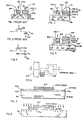
- Reference may be had to FIG. 1 wherein the prior art conventional memory cell structure is shown as comprising the
transfer gate 101 and amemory capacitor 103. A silicon substrate 105 is provided which is oxidized to form thesilicon oxide 107 underneath thegate polysilicon 109 for thegate transistor 101 and thesilicon dioxide 109 underneath the polysilicon 111 forming thecapacitor 103. Thesource region 113 and drain region 115 are doped and the capacitor structure is capable of forming the temporary junction 119 beneath thesilicon oxide layer 109 in the silicon substrate 105,which junction is in electrical connection with the drain doped region 115. - The equivalent circuit for the structure shown in FIG. 1 is shown in FIG. 3 as comprising the transfer or
gating transistor 101 and thecapacitor 103. However, the junction or inversion layer 119 beneathcapacitor 103 in the structure of FIG. 1 is only there when the positive voltage is applied to the capacitor lead 121. In contrast the structure of FIG. 2 provides apermanent junction 151 because the doped polysilicon Ilayer 153 is in direct contact with the surface of thesilicon substrate 155 and the dopant is diffused into the bulk silicon to form a junction. This same layer of poly I, shown at 153 forms the transfergate polysilicon layer 159 over a thin layer ofsilicon oxide 161. Thedoped n+ region 163 is the source and thedoped n+ region 165 is the drain which region is in electrical contact with thejunction region 151. - The thin layer of
nitride 169 forms the dielectric for the capacitance which structure is completed by the poly II layer 171. Theground lead 173 for poly II layer 171 enables the junction capacitor and the nitride capacitor to be connected in parallel, thereby considerably enhancing the capacitance obtained from the structure of FIG. 2. - The electrical circuit is shown in FIG. 4 where C2 is the combined capacitance of the junction and the nitride layer, but otherwise the circuit is the same as the memory cell circuit of FIG. 3 using
transfer gate 201 for determining access tocapacitor 203. - The mathematics applicable to the structure of FIG. 1 versus the mathematics applicable to the structure of FIG. 2 will bear out the improvement of the utilization of real estate by virtue of increased capacity obtainable from the present invention.
- Considering first the structure of FIG. 1, which is evidenced by the circuitry of FIG. 3, it must be recalled that the terminal 121 of the capacitor must be held at a positive voltage to maintain the inversion under the capacitor. With this in mind, the total capacitance per unit area is given by eov/tox + CD. εox is the permittivity of the
oxide 100, whereas toxis the thickness of the oxide. CD is the depletion layer capacity. εox/tox is therefore Cox. In the foregoing, CD, the depletion layer capacitance is very small, and C is approximately equal to C1 = εox/tox x A, where A is the area of the capacitor. - Now for purposes of comparison, the mathematics for the improved structure of FIG. 2 will be given. The total capacitance per unit area is given by Cj + C where Cj is the junction capacitance and Cn is the nitride capacitance.
Cn = εn/tn for the nitride capacitor wherein En is about two times higher than εox and tn can usually be a thinner layer than that used for an oxide capacitor, therefore enhancing the value of Cn. Cj is given by

lead 173. This arrangement provides better reliability than the conventional configuration where the top electrode 121 is connected to the most positive supply, usually Ydd, because of less severe DC supply and no field inversion problems. - It will now be appreciated that the present circuitry and method of attaining a high capacitance cell can be applied to any high density dynamic memory circuit.
- The same principles obtain in the structure of FIG. 5 which merely shows a silicon on sapphire structure patterned after the structure on silicon of FIG. 2, thus the prime of the numbers applied to the structure of FIG. 2 will be used in FIG. 5. The sapphire substrate is shown at 211 and the silicon layer at 155'. The capacitor comprises the poly I layer 153', the thin nitride layer 169', the poly II layer 171' and the grounding lead 173'.
- The transfer transistor gate comprises a silicon oxide layer 161', the source 163' and the drain 165' with the capacitor junction 151' being located beneath the poly I layer 153'. Otherwise, the principles of operation heretofore explained obtain in the structure of FIG. 5.
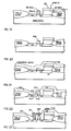
- Many existing processes will provide manufacturing methods for the present invention provided they are modified to develop the capacitive structure in conjunction with the transfer transistor gate structure. One method is illustrated in FIGs. 7 through 23 wherein a
substrate 501 of for example P(100) type silicon single or monocrystalline structure has grown thereon a thinsilicon oxide layer 503, in turn covered by anitride layer 505 and, as shown in FIG. 7.photoresist 507 defined by theactive mask 509 shown in the solid outline in FIG. 6. Thesilicon oxide coating 503 is quite thin of the order of 100 A with the silicon 0nitride coating 505 being of the order of 1000 A. The resist used inlayer 507 may be AZ 1350J or HPR204 or equivalent. - With the active area being defined by the
solid line mask 509, in FIG. 8, the field implant is shown by the xs identified at 511, theunprotected nitride 505 andsilicon oxide 503 having been removed by appropriate etching techniques, boron or the like is used here to provide a heavily doped P region surrounding the active area of a device with n+ source and drains. - In FIG. 9, the resist 507 has been removed and the field oxide grown at 513 which encircles the active region. The
field oxide 513 may have a thickness of the order of 18.6 K angstroms. - FIGURE 10 shows the outline of the capacitor region utilizing the capacitor mask -1 shown dotted at 521 in FIG. 6. First, the entire region is covered by the
photoresist 523 and thereafter themask 521 is utilized to open the region 525 to the bare silicon substrate using conventional processing techniques. - In FIG. 11 the n+ implanting of the region within
substrate 501 below bare silicon surface 525 is accomplished by ion implant or the like. Note that in FIGs. 9 and 10, thenitride layer 505 has been etched away and thephotoresist 523 applied directly to the silicon oxide layer. - In FIG. 11, the implanting is preferably carried out by a high energy ion implant. And the n+ region is indicated at 529.
- In FIG. 12, a layer of n+
doped polysilicon 531 is applied over the entire active area and is covered with a thin layer ofnitride 533. The device is subjected to high temperature to drive the dopant in to increase the depth of theregion 529. - Next, the gate capacitor mask, consisting of
dotted parts 535a and 535b in FIG. 13 is utilized to provide a resist pattern in accordance with FIG. 14 wherein the resist 537 defines the capacitive region and the resist 539, the gate region. - In FIG. 15, the nitride and doped
polysilicon layers - In FIG. 16, the resist has been removed at 537 and 539 (FIG. 15) and a thin layer of
oxide 540 grown overn+ region 529. - In FIG. 17, a layer of doped poly II
silicon 551 is applied over the entire active area. FIGURE 18 shows the capacitor mask -2, shown dotted at 553 which is used to lay down a resist pattern shown in FIG. 19 wherein the poly II 551 which is preserved will comprise the outer plate of the capacitor structure being formed. - In FIG. 20, the nitride has been removed from the
gate polysilicon layer 532 and in FIG. 21 the entire structure has been covered by a layer of phosphorus dopedglass 561. The purpose of the glass is to form a high resistivity layer over the components to isolate them when terminal connections are provided. - In FIG. 22, it may be seen that an opening has been made to the
n+ source region 541 as represented at 572. Also, anopening 573 has been made to the top of thepolysilicon 532 comprising a gate. Finally, an opening has been made to thepolysilicon 551 comprising the capacitor and is shown at 574. - These openings are filled by a metal to provide the source conductor shown at 591 in FIG. 23, the
gate conductor 592, and thecapacitance conductor 593. The latter may simply be grounded to provide the capacitive addition. - In order to form the openings described in FIG. 22, a standard opening technique is applied where masking is used to protect the remaining surface while allowing etching to take place in the areas to be opened.
- While the principles of a silicon manufacturing process have been illustrated, nevertheless many of the steps may be rearranged time wise and, accordingly, it is desired that the invention only be defined by the scope of the claims attached hereto.
- The invention may be summarized as follows:
- 1. A high capacitance memory cell comprising in combination;
- a bulk silicon wafer;
- a doped polysilicon layer adjacent a surface of the silicon wafer for forming a junction therein;
- a patterned nitride layer adjacent the doped polysilicon layer;
- a polysilicon layer adjacent the nitride layer; and,
- means for establishing electrical connection across the nitride layer.
- 2. The high capacitance memory cell of iteml, further comprising;
- a field effect transistor comprising a silicon oxide layer adjacent said surface of the silicon wafer;
- a polysilicon layer adjacent said silicon oxide layer;
- doped regions in the silicon wafer beneath opposite sides of the silicon oxide-polysilicon layers of which one region is formed by said doped polysilicon; and,
- means for establishing electrical connection to the doped region not formed by the doped polysilicon and to said polysilicon layer adjacent said silicon oxide layer.
- 3. A plurality of VLSI capacitors, each comprising in combination;
- a tiny portion of a bulk silicon wafer;
- a doped polysilicon layer portion adjacent a surface of the silicon wafer for forming an n+ junction therein;
- a patterned nitride layer portion adjacent the doped polysilicon layer;
- a polysilicon layer portion adjacent the nitride layer; and,
- means for establishing electrical connection across the nitride layer.
- 4. In combination with each of the capacitors of item 3, a high density type field effect transistor comprising in combination;
- a silicon oxide layer portion on said wafer spaced from the capacitor;
- a polysilicon layer portion on said silicon oxide layer portion for forming a gate electrode;
- a doped region within the wafer in electrical connection with said junction and extending for the length of the spacing between the silicon oxide layer and the respectively related capacitor to form a drain region;
- a further doped region within the wafer on the opposite side of the silicon oxide layer from the first mentioned doped region to comprise a source; and,
- means for establishing electrical connection to the source and gate electrode.
- 5. A VLSI capacitor comprising in combination;
- a sapphire substrate;
- a silicon layer thereon;
- a polysilicon layer adjacent the silicon layer for doping the silicon to form a junction therein;
- a nitride layer adjacent the polysilicon layer;
- a second polysilicon layer adjacent the nitride layer; and, means for establishing electrical connection across the nitride layer.
- 6. In combination with the capacitor of item 4, a high density type field effect transistor comprising in combination;
- a silicon oxide layer on said substrate spaced from the capacitor;
- a polysilicon layer on said silicon oxide layer for forming a gate electrode;
- a doped region within the silicon layer in electrical connection with said junction and extending for the length of the spacing between the silicon oxide layer and the capacitor to form a drain region;
- a further doped region within the silicon layer on the opposite side of the silicon oxide layer from the first mentioned doped region to comprise a source; and,
- means for establishing electrical connection to the source and gate electrode.
- 7. The method of making minimal area high capacitance memory cells on a semiconductor substrate to very large scale integrated circuit dimensions with each cell having a capacitor and a transistor, comprising the steps of:
- outlining active areas on the substrate by field oxide;
- growing gate oxides within said areas;
- forming openings through the gate oxides to the substrate for the capacitors;
- doping isolated regions of the substrate via said openings;
- forming a layer of doped polysilicon covered by a layer of nitride over said doped regions as a portion of a capacitor structure and at spaced locations relative thereto over the gate oxides as associated gates therefor;
- removing the gate oxide around each gate and between the gate and associated capacitor structure;
- driving dopant into the substrate through the removed gate oxide areas, which dopant on the side of the capacitor structure connects with the doped regions thereunder;
- forming layers of doped polysilicon over the nitride layers of the capacitor structures; and,
- providing electrical connections to the doped substrate adjacent the gates away from the capacitors, to the gate polysilicon layers, and to the capacitor layers of doped polysilicon over their nitride layers.
- 8. The method of item 7, wherein:
- said outlining active areas comprises growing an oxide coating on the substrate;
- depositing nitride over the oxide coating;
- masking the active areas on the nitride;
- exposing the unmasked nitride to actinic radiation; and,
- developing the exposed nitride to remove the same.
- 9. The method of making minimal area high capaci.tance memory cells on a silicon substrate to very large scale integrated circuit dimensions with each cell including a capacitor and a FET, comprising the steps of:
- outlining active areas for an associated capacitor and FET on the substrate by field oxide;
- growing gate oxides for the FETs within said areas;
- forming openings through the gate oxides to the substrate for the capacitors;
- doping isolated regions of the substrate via said openings;
- forming a layer of doped polysilicon covered by a layer of nitride at least over said doped regions as a portion of a capacitor structure and at spaced locations relative thereto over the gate oxides as associated gates therefor;
- removing the gate oxide around each gate and between the gate and the associated capacitor structure;
- driving dopant into the substrate through the areas of the substrate from which the gate oxide has been removed to define further doped regions of which one further region on the side of the capacitor structure connects with the doped regions thereunder;
- forming layers of doped polysilicon over the nitride layers of the capacitor structures;
- covering the active regions with phosphorus doped glass; and
- establishing electrical connection to the doped substrate adjacent the gates away from the capacitors, to the gate polysilicon layers, and to the capacitor layers of doped polysilicon over their nitride layers.
- 10. The method of item 9, wherein:
- the electrical connection is established by opening a hole through the phosphorus doped glass to said last mentioned doped substrate, to the gate polysilicon layer and to the doped polysilicon layer over the nitride layer for the capacitors, all in spaced apart relation for receiving electrically isolated conductors.
- 11. The method of maki.ng minimal area high capaci.tance memory cells having a single transistor including a gate and a capacitance structure on a semiconductor substrate, comprising the steps of:
- forming each gate as a layer of gate oxide on said substrate with a layer of doped polysilicon thereover and electrical connection in contact with the polysilicon;
- forming doped substrate regions on opposite sides of the gate to comprise said transistor;
- forming a further doped region in the substrate in electrical connection with a doped region on one side of the gate;
- forming electrical connection with the substrate doped region on the other side of said gate; and,
- forming the capacitance structure over the further doped region as a layer of doped polysilicon on the substrate, covered by a layer of nitride, in turn covered by a second layer of doped polysilicon with electrical connection to the latter.
- 12. The method of item 11, wherein:
- said semiconductor is P type silicon; and
- said first mentioned doped polysilicon is n+ doped.
- 13. The method of item 12, wherein:
- the doped substrate regions on opposite sides of said gate are n+ doped.
- 14. The method of item 13, wherein:
- said last mentioned layer of polysilicon is doped n+.
- 15. The method of making minimal area high capacitance memory cells comprising a capacitor and a transistor on a P doped silicon substrate, comprising the steps of:
- growing an oxide coating on the silicon substrate;
- depositing nitride over the oxide;
- applying resist over the nitride;
- masking active areas on the resist;
- removing the resist, nitride and oxide from the unmasked regions;
- implanting P doping material in the uncovered regions;
- oxidizing the substrate in the uncovered regions to form the field oxide;
- .applying resist to the oxidized substrate;
- masking the resist to outline an opening to the substrate for the capacitor structure;
- developing the resist to form said opening;
- implanting n+ doping material into the substrate via said opening;
- applying a layer of n+ doped polysilicon over the oxide on the silicon substrate, over the n+ doped region of the substrate, and over at least part of the field oxide;
- applying a thin nitride layer over the doped polysilicon;
- steaming the nitride layer to drive the dopant;
- applying resist over the nitride;
- masking the resist to outline a gate associated with a capacitive structure at least for each active area;
- exposing and developing the resist to leave spaced apart gate and capacitive resist areas;
- removing the nitride, polysilicon and oxide from the substrate where not covered by resist;
- doping n+ the substrate region on opposite sides of the gate with said doping establishing electrical connection on the side of the capacitance structure with the n+ doping material implanted via said opening;
item 15 continued- growing a thin oxide layer on the exposed substrate;
- removing the resist from the gate and capacitance structure;
- covering the active area with doped polysilicon;
- masking said n+ doped polysilicon to define the remainder of the capacitance structure;
- removing the last mentioned n+ doped polysilicon except from the capacitor;
- removing the nitride from the gate;
- covering the acti.ve region with phosphorus doped glass; and,
- establiihing electrical connections to the n+ doped region adjacent the gate but away from the capacitance structure, to the gate polysilicon, and to the capacitor last mentioned n+ doped polysilicon.
Claims (10)
1. A high capacitance memory cell comprising in combination;
a bulk silicon wafer;
a doped polysilicon layer adjacent a surface of the silicon wafer for forming a junction therein;
a patterned nitride layer adjacent the doped polysilicon layer;
a polysilicon layer adjacent the nitride layer; and,
means for establishing electrical connection across the nitride layer.
2. The high capacitance memory cell of Claim 1, further comprising;
a field effect transistor comprising a silicon oxide layer adjacent said surface of the silicon wafer;
a polysilicon layer adjacent said silicon oxide layer;
doped regions in the silicon wafer beneath opposite sides of the silicon oxide-polysilicon layers of which one region is formed by said doped polysilicon; and,
means for establishing electrical connection to the doped region not formed by the doped polysilicon and to said polysilicon layer adjacent said silicon oxide layer.
3. A plurality of VLSI capacitors, each comprising in combination;
a tiny portion of a bulk silicon wafer;
a doped polysilicon layer portion adjacent a surface of the silicon wafer for forming an n+ junction therein;
a patterned nitride layer portion adjacent the doped polysilicon layer;
a polysilicon layer portion adjacent the nitride layer; and,
means for establishing electrical connection across the nitride layer.
4. In combination with each of the capacitors of Claim 3, a high density type field effect transistor comprising in combination;
a silicon oxide layer portion on said wafer spaced from the capacitor;
a polysilicon layer portion on said silicon oxide layer portion for forming a gate electrode;
a doped region within the wafer in electrical connection with said junction and extending for the length of the spacing between the silicon oxide layer and the respectively related capacitor to form a drain region;
a further doped region within the wafer on the opposite side of the silicon oxide layer from the first mentioned doped region to comprise a source; and,
means for establishing electrical connection to the source and gate electrode.
5. A VLSI capacitor comprising in combination;
a sapphire substrate;
a silicon layer thereon;
a polysilicon layer adjacent the silicon layer for doping the silicon to form a junction therein;
a nitride layer adjacent the polysilicon layer;
a second polysilicon layer adjacent the nitride layer; and,
means for establishing electrical connection across the nitride layer.
6. In combination with the capacitor of Claim 4, a high density type field effect transistor comprising in combination;
a silicon oxide layer on said substrate spaced from the capacitor;
a polysilicon layer on said silicon oxide layer for forming a gate electrode;
a doped region within the silicon layer in electrical connection with said junction and extending for the length of the spacing between the silicon oxide layer and the capacitor to form a drain region;
a further doped region within the silicon layer on the opposite side of the silicon oxide layer from the first mentioned doped region to comprise a source; and,
means for establishing electrical connection to the source and gate electrode.
7. The method of making minimal area high capacitance memory cells on a semiconductor substrate to very large scale integrated circuit dimensions with each cell having a capacitor and a transistor, comprising the steps of:
outlining active areas on the substrate by field oxide;
growing gate oxides within said areas;
forming openings through the gate oxides to the substrate for the capacitors;
doping isolated regions of the substrate via said openings;
forming a layer of doped polysilicon covered by a layer of nitride over said doped regions as a portion of a capacitor structure and at spaced locations relative thereto over the gate oxides as associated gates therefor;
removing the gate oxide around each gate and between the gate and associated capacitor structure;
driving dopant into the substrate through the removed gate oxide areas, which dopant on the side of the capacitor structure connects with the doped regions thereunder;
forming layers of doped polysilicon over the nitride layers of the capacitor structures; and,
providing electrical connections to the doped substrate adjacent the gates away from the capacitors, to the gate polysilicon layers, and to the capacitor layers of doped polysilicon over their nitride layers.
8. The method of Claim 7, wherein:
said outlining active areas comprises growing an oxide coating on the substrate;
depositing nitride over the oxide coating;
masking the active areas on the nitride;
exposing the unmasked nitride to actinic radiation; and,
developing the exposed nitride to remove the same.
9. The method of making minimal area high capacitance memory cells on a silicon substrate to very large scale integrated circuit dimensions with each cell including a capacitor and a FET, comprising the steps of:
outlining active areas for an associated capacitor and FET on the substrate by field oxide;
growing gate oxides for the FETs within said areas;
forming openings through the gate oxides to the substrate for the capacitors;
doping isolated regions of the substrate via said openings;
forming a layer of doped polysilicon covered by a layer of nitride at least over said doped regions as a portion of a capacitor structure and at spaced locations relative thereto over the gate oxides as associated gates therefor;
removing the gate oxide around each gate and between the gate and the associated capacitor structure;
driving dopant into the substrate through the areas of the substrate from which the gate oxide has been removed to define further doped regions of which one further region on the side of the capacitor structure connects with the doped regions thereunder;
forming layers of doped polysilicon over the nitride layers of the capacitor structures;
covering the active regions with phosphorus doped glass; and
establishing electrical connection to the doped substrate adjacent the gates away from the capacitors, to the gate polysilicon layers, and to the capacitor layers of doped polysilicon over their nitride layers.
10. The method of Claim 9, wherein:
the electrical connection is established by opening a hole through the phosphorus doped glass to said last mentioned doped substrate, to the gate polysilicon layer and to the doped polysilicon layer over the nitride layer for the capacitors, all in spaced apart relation for receiving electrically isolated conductors.
Applications Claiming Priority (2)
| Application Number | Priority Date | Filing Date | Title |
|---|---|---|---|
| US21278480A | 1980-12-04 | 1980-12-04 | |
| US212784 | 1988-06-29 |
Publications (2)
| Publication Number | Publication Date |
|---|---|
| EP0053654A2 true EP0053654A2 (en) | 1982-06-16 |
| EP0053654A3 EP0053654A3 (en) | 1983-03-30 |
Family
ID=22792412
Family Applications (1)
| Application Number | Title | Priority Date | Filing Date |
|---|---|---|---|
| EP81106695A Withdrawn EP0053654A3 (en) | 1980-12-04 | 1981-08-28 | High capacitance single transistor memory cell suitable for high density ram applications |
Country Status (2)
| Country | Link |
|---|---|
| EP (1) | EP0053654A3 (en) |
| JP (1) | JPS57106162A (en) |
Cited By (2)
| Publication number | Priority date | Publication date | Assignee | Title |
|---|---|---|---|---|
| US6194274B1 (en) * | 1999-08-10 | 2001-02-27 | Winbond Electronics Corp. | Method of fabricating a mask ROM |
| US6432791B1 (en) * | 1999-04-14 | 2002-08-13 | Texas Instruments Incorporated | Integrated circuit capacitor and method |
-
1981
- 1981-08-28 EP EP81106695A patent/EP0053654A3/en not_active Withdrawn
- 1981-10-29 JP JP56175570A patent/JPS57106162A/en active Pending
Non-Patent Citations (3)
| Title |
|---|
| IBM TECHNICAL DISCLOSURE BULLETIN, Vol. 23, No. 12, May 1981, New York. P. DUN et al: "High capacitance RAM cell using two layers of polysilicon", pages 5290 to 5291 * |
| IEEE TRANSACTIONS ON ELECTRON DEVICES, Vol. ED-23, No. 10, October 1976, New York. C.G. SODINI et al: "Ehanced capacitor for one-transistor memory cell", pages 1187 to 1189 * |
| IEEE TRANSACTIONS ON ELECTRON DEVICES, Vol. ED-27, No. 8, August 1980, New York. M. KOYANAGI et al: "A 5-V only 16-kbit stacked-capacitor MOS RAM", pages 1596 to 1601 * |
Cited By (2)
| Publication number | Priority date | Publication date | Assignee | Title |
|---|---|---|---|---|
| US6432791B1 (en) * | 1999-04-14 | 2002-08-13 | Texas Instruments Incorporated | Integrated circuit capacitor and method |
| US6194274B1 (en) * | 1999-08-10 | 2001-02-27 | Winbond Electronics Corp. | Method of fabricating a mask ROM |
Also Published As
| Publication number | Publication date |
|---|---|
| JPS57106162A (en) | 1982-07-01 |
| EP0053654A3 (en) | 1983-03-30 |
Similar Documents
| Publication | Publication Date | Title |
|---|---|---|
| US4314857A (en) | Method of making integrated CMOS and CTD by selective implantation | |
| CA1079866A (en) | Fet one-device memory cells with two layers of polycrystalline silicon | |
| US5807778A (en) | Method of manufacturing shallow trench source EPROM cell | |
| US4252579A (en) | Method for making single electrode U-MOSFET random access memory utilizing reactive ion etching and polycrystalline deposition | |
| US4931847A (en) | Floating gate memory with sidewall tunnelling area | |
| US4178674A (en) | Process for forming a contact region between layers of polysilicon with an integral polysilicon resistor | |
| US4566175A (en) | Method of making insulated gate field effect transistor with a lightly doped drain using oxide sidewall spacer and double implantations | |
| US4804637A (en) | EEPROM memory cell and driving circuitry | |
| US5162890A (en) | Stacked capacitor with sidewall insulation | |
| US4717942A (en) | Dynamic ram with capacitor groove surrounding switching transistor | |
| US5668391A (en) | Vertical thin film transistor | |
| US5492851A (en) | Method for fabricating attached capacitor cells in a semiconductor device having a thin film transistor | |
| EP0511370A1 (en) | Method of making an MOS EEPROM floating gate transistor cell | |
| US5017515A (en) | Process for minimizing lateral distance between elements in an integrated circuit by using sidewall spacers | |
| EP0167764A2 (en) | Dynamic ram cell | |
| US4975383A (en) | Method for making an electrically erasable programmable read only memory cell having a three dimensional floating gate | |
| US4878100A (en) | Triple-implanted drain in transistor made by oxide sidewall-spacer method | |
| JPH03129769A (en) | Dynamic ram storge element and its manufacture | |
| EP0028654B1 (en) | Semiconductive memory device and fabricating method therefor | |
| US6040209A (en) | Semiconductor memory device and method of forming transistors in a peripheral circuit of the semiconductor memory device | |
| US5245212A (en) | Self-aligned field-plate isolation between active elements | |
| EP0034508A1 (en) | Self-aligned buried contact and method of making | |
| US4357747A (en) | Method for producing a semiconductor device having an insulated gate type field effect transistor | |
| EP0053654A2 (en) | High capacitance single transistor memory cell suitable for high density RAM applications | |
| KR100261210B1 (en) | Method for manufacturing decoupling capacitor |
Legal Events
| Date | Code | Title | Description |
|---|---|---|---|
| PUAI | Public reference made under article 153(3) epc to a published international application that has entered the european phase |
Free format text: ORIGINAL CODE: 0009012 |
|
| 17P | Request for examination filed |
Effective date: 19811023 |
|
| AK | Designated contracting states |
Designated state(s): DE FR GB IT |
|
| PUAL | Search report despatched |
Free format text: ORIGINAL CODE: 0009013 |
|
| AK | Designated contracting states |
Designated state(s): DE FR GB IT |
|
| STAA | Information on the status of an ep patent application or granted ep patent |
Free format text: STATUS: THE APPLICATION IS DEEMED TO BE WITHDRAWN |
|
| 18D | Application deemed to be withdrawn |
Effective date: 19850302 |
|
| RIN1 | Information on inventor provided before grant (corrected) |
Inventor name: TAM, MATTHIAS LAPKAY Inventor name: CUSTODE, FRANK ZUCHOV |