EP0045877A1 - Laminated ceramic sheet printed circuit components including capacitance means - Google Patents
Laminated ceramic sheet printed circuit components including capacitance means Download PDFInfo
- Publication number
- EP0045877A1 EP0045877A1 EP81105736A EP81105736A EP0045877A1 EP 0045877 A1 EP0045877 A1 EP 0045877A1 EP 81105736 A EP81105736 A EP 81105736A EP 81105736 A EP81105736 A EP 81105736A EP 0045877 A1 EP0045877 A1 EP 0045877A1
- Authority
- EP
- European Patent Office
- Prior art keywords
- ceramic
- carrier
- chip
- capacitors
- printed circuit
- Prior art date
- Legal status (The legal status is an assumption and is not a legal conclusion. Google has not performed a legal analysis and makes no representation as to the accuracy of the status listed.)
- Granted
Links
Images


Classifications
-
- H—ELECTRICITY
- H01—ELECTRIC ELEMENTS
- H01L—SEMICONDUCTOR DEVICES NOT COVERED BY CLASS H10
- H01L23/00—Details of semiconductor or other solid state devices
- H01L23/58—Structural electrical arrangements for semiconductor devices not otherwise provided for, e.g. in combination with batteries
- H01L23/64—Impedance arrangements
- H01L23/642—Capacitive arrangements
-
- H—ELECTRICITY
- H01—ELECTRIC ELEMENTS
- H01L—SEMICONDUCTOR DEVICES NOT COVERED BY CLASS H10
- H01L23/00—Details of semiconductor or other solid state devices
- H01L23/12—Mountings, e.g. non-detachable insulating substrates
- H01L23/14—Mountings, e.g. non-detachable insulating substrates characterised by the material or its electrical properties
- H01L23/15—Ceramic or glass substrates
-
- H—ELECTRICITY
- H01—ELECTRIC ELEMENTS
- H01L—SEMICONDUCTOR DEVICES NOT COVERED BY CLASS H10
- H01L23/00—Details of semiconductor or other solid state devices
- H01L23/52—Arrangements for conducting electric current within the device in operation from one component to another, i.e. interconnections, e.g. wires, lead frames
- H01L23/538—Arrangements for conducting electric current within the device in operation from one component to another, i.e. interconnections, e.g. wires, lead frames the interconnection structure between a plurality of semiconductor chips being formed on, or in, insulating substrates
- H01L23/5383—Multilayer substrates
-
- H—ELECTRICITY
- H05—ELECTRIC TECHNIQUES NOT OTHERWISE PROVIDED FOR
- H05K—PRINTED CIRCUITS; CASINGS OR CONSTRUCTIONAL DETAILS OF ELECTRIC APPARATUS; MANUFACTURE OF ASSEMBLAGES OF ELECTRICAL COMPONENTS
- H05K1/00—Printed circuits
- H05K1/16—Printed circuits incorporating printed electric components, e.g. printed resistor, capacitor, inductor
- H05K1/162—Printed circuits incorporating printed electric components, e.g. printed resistor, capacitor, inductor incorporating printed capacitors
-
- H—ELECTRICITY
- H01—ELECTRIC ELEMENTS
- H01L—SEMICONDUCTOR DEVICES NOT COVERED BY CLASS H10
- H01L2224/00—Indexing scheme for arrangements for connecting or disconnecting semiconductor or solid-state bodies and methods related thereto as covered by H01L24/00
- H01L2224/01—Means for bonding being attached to, or being formed on, the surface to be connected, e.g. chip-to-package, die-attach, "first-level" interconnects; Manufacturing methods related thereto
- H01L2224/10—Bump connectors; Manufacturing methods related thereto
- H01L2224/15—Structure, shape, material or disposition of the bump connectors after the connecting process
- H01L2224/16—Structure, shape, material or disposition of the bump connectors after the connecting process of an individual bump connector
-
- H—ELECTRICITY
- H01—ELECTRIC ELEMENTS
- H01L—SEMICONDUCTOR DEVICES NOT COVERED BY CLASS H10
- H01L2924/00—Indexing scheme for arrangements or methods for connecting or disconnecting semiconductor or solid-state bodies as covered by H01L24/00
- H01L2924/01—Chemical elements
- H01L2924/01014—Silicon [Si]
-
- H—ELECTRICITY
- H01—ELECTRIC ELEMENTS
- H01L—SEMICONDUCTOR DEVICES NOT COVERED BY CLASS H10
- H01L2924/00—Indexing scheme for arrangements or methods for connecting or disconnecting semiconductor or solid-state bodies as covered by H01L24/00
- H01L2924/01—Chemical elements
- H01L2924/01019—Potassium [K]
-
- H—ELECTRICITY
- H01—ELECTRIC ELEMENTS
- H01L—SEMICONDUCTOR DEVICES NOT COVERED BY CLASS H10
- H01L2924/00—Indexing scheme for arrangements or methods for connecting or disconnecting semiconductor or solid-state bodies as covered by H01L24/00
- H01L2924/01—Chemical elements
- H01L2924/01046—Palladium [Pd]
-
- H—ELECTRICITY
- H01—ELECTRIC ELEMENTS
- H01L—SEMICONDUCTOR DEVICES NOT COVERED BY CLASS H10
- H01L2924/00—Indexing scheme for arrangements or methods for connecting or disconnecting semiconductor or solid-state bodies as covered by H01L24/00
- H01L2924/01—Chemical elements
- H01L2924/01068—Erbium [Er]
-
- H—ELECTRICITY
- H01—ELECTRIC ELEMENTS
- H01L—SEMICONDUCTOR DEVICES NOT COVERED BY CLASS H10
- H01L2924/00—Indexing scheme for arrangements or methods for connecting or disconnecting semiconductor or solid-state bodies as covered by H01L24/00
- H01L2924/01—Chemical elements
- H01L2924/01079—Gold [Au]
-
- H—ELECTRICITY
- H01—ELECTRIC ELEMENTS
- H01L—SEMICONDUCTOR DEVICES NOT COVERED BY CLASS H10
- H01L2924/00—Indexing scheme for arrangements or methods for connecting or disconnecting semiconductor or solid-state bodies as covered by H01L24/00
- H01L2924/095—Indexing scheme for arrangements or methods for connecting or disconnecting semiconductor or solid-state bodies as covered by H01L24/00 with a principal constituent of the material being a combination of two or more materials provided in the groups H01L2924/013 - H01L2924/0715
- H01L2924/097—Glass-ceramics, e.g. devitrified glass
- H01L2924/09701—Low temperature co-fired ceramic [LTCC]
-
- H—ELECTRICITY
- H01—ELECTRIC ELEMENTS
- H01L—SEMICONDUCTOR DEVICES NOT COVERED BY CLASS H10
- H01L2924/00—Indexing scheme for arrangements or methods for connecting or disconnecting semiconductor or solid-state bodies as covered by H01L24/00
- H01L2924/10—Details of semiconductor or other solid state devices to be connected
- H01L2924/102—Material of the semiconductor or solid state bodies
- H01L2924/1025—Semiconducting materials
- H01L2924/10251—Elemental semiconductors, i.e. Group IV
- H01L2924/10253—Silicon [Si]
-
- H—ELECTRICITY
- H01—ELECTRIC ELEMENTS
- H01L—SEMICONDUCTOR DEVICES NOT COVERED BY CLASS H10
- H01L2924/00—Indexing scheme for arrangements or methods for connecting or disconnecting semiconductor or solid-state bodies as covered by H01L24/00
- H01L2924/15—Details of package parts other than the semiconductor or other solid state devices to be connected
- H01L2924/151—Die mounting substrate
- H01L2924/153—Connection portion
- H01L2924/1531—Connection portion the connection portion being formed only on the surface of the substrate opposite to the die mounting surface
- H01L2924/15311—Connection portion the connection portion being formed only on the surface of the substrate opposite to the die mounting surface being a ball array, e.g. BGA
-
- H—ELECTRICITY
- H01—ELECTRIC ELEMENTS
- H01L—SEMICONDUCTOR DEVICES NOT COVERED BY CLASS H10
- H01L2924/00—Indexing scheme for arrangements or methods for connecting or disconnecting semiconductor or solid-state bodies as covered by H01L24/00
- H01L2924/15—Details of package parts other than the semiconductor or other solid state devices to be connected
- H01L2924/151—Die mounting substrate
- H01L2924/153—Connection portion
- H01L2924/1531—Connection portion the connection portion being formed only on the surface of the substrate opposite to the die mounting surface
- H01L2924/15312—Connection portion the connection portion being formed only on the surface of the substrate opposite to the die mounting surface being a pin array, e.g. PGA
-
- H—ELECTRICITY
- H05—ELECTRIC TECHNIQUES NOT OTHERWISE PROVIDED FOR
- H05K—PRINTED CIRCUITS; CASINGS OR CONSTRUCTIONAL DETAILS OF ELECTRIC APPARATUS; MANUFACTURE OF ASSEMBLAGES OF ELECTRICAL COMPONENTS
- H05K1/00—Printed circuits
- H05K1/02—Details
- H05K1/03—Use of materials for the substrate
- H05K1/0306—Inorganic insulating substrates, e.g. ceramic, glass
-
- H—ELECTRICITY
- H05—ELECTRIC TECHNIQUES NOT OTHERWISE PROVIDED FOR
- H05K—PRINTED CIRCUITS; CASINGS OR CONSTRUCTIONAL DETAILS OF ELECTRIC APPARATUS; MANUFACTURE OF ASSEMBLAGES OF ELECTRICAL COMPONENTS
- H05K1/00—Printed circuits
- H05K1/02—Details
- H05K1/09—Use of materials for the conductive, e.g. metallic pattern
- H05K1/092—Dispersed materials, e.g. conductive pastes or inks
-
- H—ELECTRICITY
- H05—ELECTRIC TECHNIQUES NOT OTHERWISE PROVIDED FOR
- H05K—PRINTED CIRCUITS; CASINGS OR CONSTRUCTIONAL DETAILS OF ELECTRIC APPARATUS; MANUFACTURE OF ASSEMBLAGES OF ELECTRICAL COMPONENTS
- H05K2201/00—Indexing scheme relating to printed circuits covered by H05K1/00
- H05K2201/09—Shape and layout
- H05K2201/09209—Shape and layout details of conductors
- H05K2201/09654—Shape and layout details of conductors covering at least two types of conductors provided for in H05K2201/09218 - H05K2201/095
- H05K2201/09763—Printed component having superposed conductors, but integrated in one circuit layer
-
- H—ELECTRICITY
- H05—ELECTRIC TECHNIQUES NOT OTHERWISE PROVIDED FOR
- H05K—PRINTED CIRCUITS; CASINGS OR CONSTRUCTIONAL DETAILS OF ELECTRIC APPARATUS; MANUFACTURE OF ASSEMBLAGES OF ELECTRICAL COMPONENTS
- H05K3/00—Apparatus or processes for manufacturing printed circuits
- H05K3/46—Manufacturing multilayer circuits
- H05K3/4611—Manufacturing multilayer circuits by laminating two or more circuit boards
- H05K3/4626—Manufacturing multilayer circuits by laminating two or more circuit boards characterised by the insulating layers or materials
- H05K3/4629—Manufacturing multilayer circuits by laminating two or more circuit boards characterised by the insulating layers or materials laminating inorganic sheets comprising printed circuits, e.g. green ceramic sheets
Definitions
- This invention relates to laminated ceramic sheet printed circuit devices including capacitance means, for example, carriers for supporting integrated circuit chips.
- an object of this invention is to provide a laminated ceramic sheet printed circuit integrated chip carrier or interposer with built in capacitance having a large value of capacitance, and a low and well matched coefficient of thermal expansion for the entire structure to minimize mechanical stresses caused by mismatch of coefficients of thermal expansion between the materials of the structure.
- Another object of this invention is to provide a laminated ceramic sheet printed circuit device with a high value of capacitance, minimal inductance, and an integral structure with minimum stress composed of a large number of individual capacitors which preferably are connected in parallel.
- Laminated ceramic sheet printed circuit device including capacitance means formed from printed circuitry and dielectric material having a substantially higher dielectric constant than that of the ceramic sheets is characterised according to the invention by the higher dielectric constant material of the capacitance means being in the form of a matrix of disc-shaped bits of material so disposed within the device that the device has a coefficient of thermal expansion which is substantially the same as that of the ceramic sheet material and is a satisfactory match to that of a silicon integrated circuit chip.
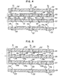
- F I G. 1 shows a sectional view of a multilayered ceramic chip carrier 1 carrying a chip 11.
- Chip 11 is supported by means of C-4 solder balls bonded to conductor pads 15 which are connected to conductive vias 45 which rest upon conductive straps 44 which extend back into the page of the drawing to connect to other vias.
- Straps 44 are connected to respective vias 5, 6, 7 and 8 which extend down to straps 41, 42 and 43 which also extend into the page to provide interconnections between vias and pins 17.
- Other vias 4 and 5 extend directly from straps 44 or other metal lines to pins 17 via pads 3 upon which pins 17 are brazed.
- carrier 1 is a laminated arrangement of ceramic sheets 2 into which metal conductors and capacitors 9 are included to provide a chip carrier with maximum capacitance, minimal inductance and short connection lines with low resistance. Stacked layers of arrays of capacitors 9' are interconnected as desired with the vias 5, 6, 7, and 8 as illustrated in a simplified way in FIG. 1. Because the capacitors are very small and occupy a small volume of the overall carrier, they do not affect the overall thermal expansion characteristics of the carrier adversely. In addition, because there are so many of the capacitors in the carrier, there is a large total value of capacitance. This is explained below in greater detail with reference to FIGS. 1 and 2.
- the pads 15 are connected (not shown) to signal lines x and y of fan-out metallurgy 40 in a conventional fashion.
- the x and y thin film metallization is within the layer 46 just beneath the upper surface of the carrier 1.
- interposer structures 10 are shown carrying "Large Scale Integrated” (LSI) circuit silicon chips 11.
- interposer structures 10 are carried on a ceramic substrate 12.
- Solder ball joints 14 (known as C-4 joints) are employed to bond chips 11 to interposer structures 10.
- Solder ball joints 18 bond interposer structures 10 to substrate 12 in a conventional manner.
- the solder ball joints 14 of chip 11 rest upon pads 15 on the interposer structures 10.
- Joints 18 rest on pads 16 on the substrate 12.
- Upon the lower surface of substrate 12 are pins 17 adapted to be inserted into receptacles in an even larger circuit board, not shown.
- the interposer structures 10 are required to provide (a) mechanical support for chips 11 mounted by joints 14 and (b) a capacitance per chip of about 20 nf (10 -9 farads) per chip. There are similar requirements for carrier 1 in FIG. 1.
- the interposer or chip carrier structure To satisfy requirement (a), it is necessary for the interposer or chip carrier structure to have a relatively low "coefficient of thermal expansion" (a) close to that of the silicon material of which the chips 11 are composed.
- the value of the coefficient of expansion of the interposer structure 10 or carrier 1 is between that of silicon and that of the substrate 12 which is principally composed of materials such as alumina and silica.
- the a of silicon is 3 x 10 -6 per °C and that of substrate 12 is about 6 x 10 -6 per ° C if it is composed of alumina and silica.
- ⁇ r a high "dielectric constant" ( ⁇ r ) is necessary to provide the required capacitance in the geometrical configuration of the carrier 1 or the interposer structure 10.
- High e materials such as barium or strontium titanates have a values of about 10 x 10 per °C.
- the main structure of the carrier 1 connected to C-4 joints or the interposer 10 connected to the solder ball joints 14 and 18 retains the low a of the low ⁇ r material, yet it has the required value of capacitance.
- FIG. 4 an exploded sectional view is shown of a stack of ceramic sheets 128, 120, 127 and 131 with space indicated between sheets 127 and 131 to indicate that there can be included numerous other layers. Numerous layers identical to layers 120 and 127 are to be placed in that array alternately to form capacitors between sheets 128 and 131.
- the green sheets from which layers 120 and 127 were formed were perforated (as are sheets 20 in F IG. 8 as described below).
- a metal paste is deposited to form vias 129, 130 and 133 and contact pads 129', 130' and 133'. When the sheets are assembled, through vias are formed and contacts are formed for providing electrical connections to the capacitors formed in the sheets 120 and 127.
- a high dielectric constant material 122 which is sandwiched between conductor layers 124, 125 and 132, thereby forming capacitors in a matrix which extends back into the page and which extends to the right and the left for some distance as far as required and down several layers to whatever depth is required.
- the pads 129', 133' and 130' are shown at voltages V 1 negative, V 2 positive and V 3 negative as an example of the values of the bias voltages which might be applied to the various terminals of the capacitors formed in the stack of ceramic sheets.
- Conductor 125 is shown on the upper surface of the layer 127 connecting the via 129 to the capacitor elements formed by dielectric 122 in perforation 121 and conductors 125, 124, and 132. Similarly, the conductor 125' connects to other dielectric elements 122 adjacent to via 130. Conductors 125 and 125' complement conductors 124 and 132.
- FIG. 5 is an exploded view of the modified capacitor array of FIG. 4 wherein the perforations 221a in the green sheets 228, 220, 227 and 231 are all filled with metal for vias 229, 229a, 233, 230 and 230a.
- the high dielectric constant material 222 is placed between the conductor 224 (connected to via 233 and lands 233') and the lands 229' and 230' of vias 229a and 230a which are connected to vias 229 and 230 by means of conductors 225 and 225' on green sheet 227.
- the capacitors are formed between the layers 220 and 228 of ceramic material. Again, the section shown in FIG.
- FI G. 6.1 shows a perspective view of one capacitive element of a matrix of capacitive elements in a laminated ceramic sheet printed circuit device in accordance with this invention where the capacitive elements are formed between the ceramic layers.
- the dielectric layer 322 is sandwiched between two metallic layers 324' and 325 as shown in greater detail in FIG. 6.2.
- the electrodes 324' and 325 are connected to conductive vias 330 and 333 as shown in FIG. 6.2 also.
- FIG. 6.2 there are several ceramic layers 328, 320, 327 and 331 with a number of pairs of layers 320 and 327 with as many as required to achieve the quantity of capacitance required.
- Vias 329, 333 and 330 are arranged similarly to those above with the pads 329 1 , 333' and 330' analogous as well.
- On the left and right sides on the lower surface of layer 320 are metallic layers 324 and 324' which sandwich the dielectric dots 322 beneath them. The dots 322 rest upon metallization layer 325 which forms the other electrode plate of the two capacitors shown.
- Metallization 325 is connected to vias 333 by means of one of the pads 333'.
- all of the capacitor materials between the ceramic layers are screened onto the ceramic layers through silk screen masks. That is, layers 324, 324' of metal on ceramic substrate 320 and metallization 325 and dielectric material 322 are screened upon the upper surface of ceramic substrate 327.
- FIG. 7.1 shows an exploded view of a ceramic carrier comprising ceramic sheets 428, 420, 427, 431 and containing a capacitor matrix according to the format of FIG. 4 with the modification that the ceramic capacitors are formed between the multiple ceramic layers (e.g. 420, 427) and that a void or partially filled space is formed above and below each of the capacitors.
- FIG. 6.2 there is a sandwich of a conductor 424, a dielectric 422 and a lower conductor 425.
- volatile or partially volatile paste 450 which is shown in FIG. 7.2. as a void 460 in the assembled and fired carrier structure.
- the interposer structure 10 of FIG. 2 can be fabricated by means of a "multilayered ceramic” (MLC) technology.
- MLC multilayered ceramic
- FIG. 9 another screening operation is employed to deposit metal filled paste to form a blanket metallic capacitor plate (electrode) 24 over the area in which high E material forming discs 22 was deposited in holes 21 as shown in FIG. 9.
- This screening process also fills holes 21a with vias 29 and 30 of metal filled paste in the pattern shown and provides pads 29' above vias 29. The same process applies to holes 21a in layer 27 in FIG. 10, in reverse from left to right.
- a capacitor structure is fabricated by stacking several sheets 28 (top), 20 and 27 (middle-right to left mirror image) and 31 (bottom) at least.
- the top sheet 28 consists of a ceramic sheet with electrical vias 29 and 30 connected to electrode pads 29' and 30'.
- sheet 28 includes no dielectric discs 22.
- Several high E r filled sheets 20 of the variety shown in FIG. 9 are included in the structure.
- sheets 27 which are the mirror image of sheets 20 are stacked alternately with sheets 20.
- Metal plates 24 on sheets 20 are connected to electrodes 30' and vias 30 respectively below and above.
- Metal capacitor plates 25 are connected to vias 29 below and above, which connect to electrode pads 29'.
- Electrode pads 29' and vias 29 and electrode pads 30' and vias 30 extend from sheet to sheet to form an overall via 29 and an overall via 30 at each site with the interior vias connecting the other vias together by providing a large enough surface to correct for misalignment of the vias and the electrode pads 29' and 30'.
- a bottom sheet 31 is screened with a metal layer 32 to form the bottom capacitor plate, and it connects to vias 30 above and below. Via 30 connects to an electrode pad 30' on the lower surface of sheet 31. Vias 29 are provided on the left end with a pair of electrode pads 29' above and below. Sheet 31 includes no dielectric discs (dots) 22.
- the composite structure is then sintered in an appropriate ambient atmosphere compatible with both high and low ⁇ r materials and metal.
- the capacitance of a 30 x 30 matrix of holes is about 10 nf per layer. Success using this approach requires avoiding air or low ⁇ gaps at the metal-ceramic interfaces. This problem does not usually arise since relatively ductile metals will conform to the relatively small distortions (less than 1 ⁇ m) if good metal-to-ceramic adhesion is attained.
- F IG . 12 shows a multilayered ceramic capacitor 70 which employs a matrix of holes into which high dielectric constant material is inserted to provide high capacitance. Thin layers of metal serving as electrodes are deposited upon the interfaces between layers of ceramic material as the capacitor is being assembled. Solder balls 96, 97, 98 and 99 are illustrative of the C-4 solder ball array which is employed to connect to a chip carrier.
- the capacitor 70 is adapted for attachment to the upper surface of a chip carrier such as carrier 12 or even an interposer 10 in FIG. 2.
- FIG. 13 shows a sectional view of the capacitor of FIG. 12 taken along line FIG. 13- FIG . 13 in F IG. 12.
- solder balls 96, 97, 98 and 99 are shown at the base of the capacitor.
- electrode 90 which is designated - to indicate polarity.
- solder ball 97 which is designated + to indicate positive electrical polarity is a pair of capacitor plates 91 and 92 which are deposited upon opposite surfaces of a ceramic layer 83. The plates 91 and 92 are thus connected to the same polarity.
- ceramic layer 86 (perforated and containing dielectric discs 22) is between plate 94 and plate 95. Plate 95 is connected to positive solder ball 99.
- the next ceramic layer is layer 87 laminated to plate 95, and the last ceramic layer is layer 88.
- plates 90-95 there are extensions as can be seen by reference to FI G . 14 wherein the extension of plate 90 is tab 101, and the extensions of plates 91, 92 and 93 are tabs 102, 103 and 104 respectively. It can be seen that plates 91 and 92 are connected in FIG. 13 by means of a half-disc 100 which bridges the space between tabs 102 and 103. Additional discs 100 are shown in FIG. 13 for the purpose of connecting plate 90 to solder ball 96, plate 93 and plate 94 to solder ball 98 and for connecting plate electrode 95 to solder ball 99.
- disc 100 can be extended across to join several sets of capacitor plates if the tabs extending therefrom are staggered.
Abstract
Description
- This invention relates to laminated ceramic sheet printed circuit devices including capacitance means, for example, carriers for supporting integrated circuit chips.
- The principal problem solved by this invention is the provision of relatively high capacitance in a laminated ceramic sheet printed circuit device having a coefficient of thermal expansion which is a satisfactory match to that of a silicon integrated circuit chip. Thus, an object of this invention is to provide a laminated ceramic sheet printed circuit integrated chip carrier or interposer with built in capacitance having a large value of capacitance, and a low and well matched coefficient of thermal expansion for the entire structure to minimize mechanical stresses caused by mismatch of coefficients of thermal expansion between the materials of the structure.
- Another object of this invention is to provide a laminated ceramic sheet printed circuit device with a high value of capacitance, minimal inductance, and an integral structure with minimum stress composed of a large number of individual capacitors which preferably are connected in parallel.
- Laminated ceramic sheet printed circuit device including capacitance means formed from printed circuitry and dielectric material having a substantially higher dielectric constant than that of the ceramic sheets is characterised according to the invention by the higher dielectric constant material of the capacitance means being in the form of a matrix of disc-shaped bits of material so disposed within the device that the device has a coefficient of thermal expansion which is substantially the same as that of the ceramic sheet material and is a satisfactory match to that of a silicon integrated circuit chip.
- How the invention can be carried out will now be described by way of example, with reference to the accompanying drawings, in which :-
- FIG. 1 is a sectional view of a chip carrier including an array of capacitors, in accordance with this invention;
- FIG. 2 represents an end view of a chip carrier upon which a pair of interposer structures are mounted carrying VLSI semiconductor chips;
- FIG. 3 is a graph of normalized values of the dielectric constant E and coefficient of thermal expansion a as a function of percentage composition of two materials of opposite varieties with high dielectric constant and also a high coefficient of thermal expansion at one end and low values of the dielectric constant and the coefficient of thermal expansion at the other end;
- FIG. 4 is an exploded sectional view, prior to lamination, of a chip carrier in accordance with this invention comprising a plurality of ceramic sheets with associated vias and connectors composed of metal plus high dielectric constant discs which reside in holes in the ceramic sheets, providing an array of capacitors on multiple levels in the structure;
- FIG. 5 is a modified form (shown prior to lamination) of the carrier of FIG. 4 wherein the capacitors in the structure are formed by metal discs formed in apertures or holes in the ceramic sheets capped by high dielectric constant discs with electrodes upon the other surface thereof completing the capacitors;
- FIG. 6.1 is a perspective view of a laminated third form of capacitor in accordance with the concept of FIG. 1 and applicable in a modification of the structures of FIGS. 4 and 5 wherein the capacitors are formed by laminating metallic and dielectric layers between the ceramic green sheets prior to firing for forming an array of capacitor elements within the structure;
- FIG. 6.2 shows the capacitor structure, prior to lamination, employing capacitors in accordance with FIG. 6.1 in an exploded sectional view similar to those of FIGS. 4 and 5;
- FIG. 7.1 shows a similar view to FIGS. 4, 5, and 6.2 for an unfired, unlaminated modification of the array of capacitors in a chip carrier segment wherein the capacitors are formed between green sheets with volatile or-partially volatile paste layers filled with inert particles above and below;
- FIG. 7.2 shows the structure of FIG. 7.1 after firing with voids or partially filled voids provided above and below the capacitors where the volatile portion of the paste has been driven off during firing of the green sheets of ceramic material;
- FIG. 8 shows a sectioned perspective view of a perforated sheet for use on a chip carrier or interposer with discs of high dielectric material inserted into some of the perforations;
- FIG. 9 is a view of the structure of FIG. 8 after it has been further processed to include metallization upon the upper surface of the sheet, where desired, which is applied in the form of a metal filled paste which fills the remaining perforations and covers the sections where a capacitor plate is desired to be located;
- FIG. 10 is an exploded view of an assembly comprising a number of ceramic sheets, each of which has been processed to acquire a structure similar to that shown in FIG. 9, for forming a multilayered ceramic capacitor;
- FIG. 11 represents an elevation of the assembly of FIG. 10;
- FIG. 12 represents a vertically oriented multilayered ceramic capacitor structure in accordance with this invention;
- FIG. 13 is a section taken on line FIG. 13-FIG. 13 in FIG. 12; and
- FIG. 14 is an exploded view of a portion of the vertical capacitor of FIGS. 12 and 13.
- FIG. 1 shows a sectional view of a multilayered
ceramic chip carrier 1 carrying achip 11.Chip 11 is supported by means of C-4 solder balls bonded toconductor pads 15 which are connected toconductive vias 45 which rest uponconductive straps 44 which extend back into the page of the drawing to connect to other vias.Straps 44 are connected torespective vias straps pins 17.Other vias 4 and 5 extend directly fromstraps 44 or other metal lines topins 17 via pads 3 upon whichpins 17 are brazed. The basic structure ofcarrier 1 is a laminated arrangement ofceramic sheets 2 into which metal conductors andcapacitors 9 are included to provide a chip carrier with maximum capacitance, minimal inductance and short connection lines with low resistance. Stacked layers of arrays of capacitors 9' are interconnected as desired with thevias carrier 1, some of thepads 15 are connected (not shown) to signal lines x and y of fan-outmetallurgy 40 in a conventional fashion. The x and y thin film metallization is within thelayer 46 just beneath the upper surface of thecarrier 1. - In FIG. 2
interposer structures 10 are shown carrying "Large Scale Integrated" (LSI)circuit silicon chips 11. Inturn interposer structures 10 are carried on aceramic substrate 12. Solder ball joints 14 (known as C-4 joints) are employed to bondchips 11 to interposerstructures 10.Solder ball joints 18bond interposer structures 10 tosubstrate 12 in a conventional manner. Thesolder ball joints 14 ofchip 11 rest uponpads 15 on theinterposer structures 10.Joints 18 rest onpads 16 on thesubstrate 12. Upon the lower surface ofsubstrate 12 arepins 17 adapted to be inserted into receptacles in an even larger circuit board, not shown. - The
interposer structures 10 are required to provide (a) mechanical support forchips 11 mounted byjoints 14 and (b) a capacitance per chip of about 20 nf (10-9 farads) per chip. There are similar requirements forcarrier 1 in FIG. 1. - To satisfy requirement (a), it is necessary for the interposer or chip carrier structure to have a relatively low "coefficient of thermal expansion" (a) close to that of the silicon material of which the
chips 11 are composed. Preferably, the value of the coefficient of expansion of theinterposer structure 10 orcarrier 1 is between that of silicon and that of thesubstrate 12 which is principally composed of materials such as alumina and silica. The a of silicon is 3 x 10⁻⁶ per °C and that ofsubstrate 12 is about 6 x 10⁻⁶ per °C if it is composed of alumina and silica. - To satisfy requirement (b), a high "dielectric constant" (εr) is necessary to provide the required capacitance in the geometrical configuration of the
carrier 1 or theinterposer structure 10. High e materials such as barium or strontium titanates have a values of about 10 x 10 per °C. - A dilemma is presented because the materials which satisfy requirement (a) conflict with requirement (b). Attempts to mix particles of material with a high εr and a high a with particles of a material with a low εr and a low a have not been successful. As the low εr and low a material is added to the high εr and high a material, there is a more rapid decrease in the εr of the composite mixed materials (the
carrier 1 or the interposer structure 10) than the decrease in the a value (see FIG. 3). The cause of the more rapid decrease in the εr of the composite material is dilution which can be explained by analogy to the connection of a capacitor CHi of high εr in series with a capacitor C of low εr. For example,
- The effective capacitance Cmix is primarily attributable to the low εr capacitor. For example, if CHi = 1000 and CLo = 10, then C . = 9.90 which is extremely close to 10 but slightly below it. mix In other words, the low εr material in a matrix strongly influences the effective εr of the matrix. Other attempts to fabricate the capacitor by depositing thin (e.g., micro-meter or thinner) layers of metal/high εr material/metal on a low expansion substrate have failed because of cracking, pinholes, and low reliabity.
- In accordance with this invention, with respect to the main structure of the
carrier 1 connected to C-4 joints or theinterposer 10 connected to thesolder ball joints - Referring to FIG. 4, an exploded sectional view is shown of a stack of
ceramic sheets sheets layers sheets layers sheets 20 in FIG. 8 as described below). Into certain of theperforations 121a a metal paste is deposited to form vias 129, 130 and 133 and contact pads 129', 130' and 133'. When the sheets are assembled, through vias are formed and contacts are formed for providing electrical connections to the capacitors formed in thesheets perforations 121, which are arranged in a predetermined pattern, is deposited a high dielectricconstant material 122 which is sandwiched between conductor layers 124, 125 and 132, thereby forming capacitors in a matrix which extends back into the page and which extends to the right and the left for some distance as far as required and down several layers to whatever depth is required. The pads 129', 133' and 130' are shown at voltages V1 negative, V2 positive and V3 negative as an example of the values of the bias voltages which might be applied to the various terminals of the capacitors formed in the stack of ceramic sheets.Conductor 125 is shown on the upper surface of thelayer 127 connecting the via 129 to the capacitor elements formed by dielectric 122 inperforation 121 andconductors dielectric elements 122 adjacent to via 130.Conductors 125 and 125'complement conductors - FIG. 5 is an exploded view of the modified capacitor array of FIG. 4 wherein the
perforations 221a in thegreen sheets vias constant material 222 is placed between the conductor 224 (connected to via 233 and lands 233') and the lands 229' and 230' of vias 229a and 230a which are connected tovias conductors 225 and 225' ongreen sheet 227. In this case, the capacitors are formed between thelayers layers lower layer 231 would be required since the actual capacitors are formed by the three upper layers shown in FIG. 5. - FIG. 6.1 shows a perspective view of one capacitive element of a matrix of capacitive elements in a laminated ceramic sheet printed circuit device in accordance with this invention where the capacitive elements are formed between the ceramic layers. The
dielectric layer 322 is sandwiched between twometallic layers 324' and 325 as shown in greater detail in FIG. 6.2. Theelectrodes 324' and 325 are connected toconductive vias - In FIG. 6.2, there are several
ceramic layers layers Vias pads 3291, 333' and 330' analogous as well. On the left and right sides on the lower surface oflayer 320 aremetallic layers 324 and 324' which sandwich thedielectric dots 322 beneath them. Thedots 322 rest uponmetallization layer 325 which forms the other electrode plate of the two capacitors shown.Metallization 325 is connected tovias 333 by means of one of the pads 333'. In this embodiment, all of the capacitor materials between the ceramic layers are screened onto the ceramic layers through silk screen masks. That is, layers 324, 324' of metal onceramic substrate 320 andmetallization 325 anddielectric material 322 are screened upon the upper surface ofceramic substrate 327. - FIG. 7.1 shows an exploded view of a ceramic carrier comprising
ceramic sheets conductor 424, a dielectric 422 and alower conductor 425. Above and below the conductors is volatile or partiallyvolatile paste 450 which is shown in FIG. 7.2. as a void 460 in the assembled and fired carrier structure. - The
interposer structure 10 of FIG. 2 can be fabricated by means of a "multilayered ceramic" (MLC) technology. A method of depositing signal lines, via interconnections, etc. to form a structure generally similar to the structure of FIG. 4 will now be described - with reference to FIGS. 8 to 11. - A. Referring to FIGS. 8 and 9, in the first step of manufacturing the
structure 10 green (unfired)ceramic sheets 20 of soft pliable material about 0.10 mm thick are punched withholes holes 21a are spaced farther apart to provide electrical contact throughmetallic electrode vias 29 and 30 (in FIG. 9). Theholes 21 are then filled with a dielectric paste to formdielectric discs 22 made of a high εr material as shown in FIG. 3. A screening process is used to squeegee the dielectric paste to formdiscs 22 through a hole in a mask into theholes 21 ofgreen sheet 20. Then the dielectric paste is allowed to dry.Holes 21a are protected by the mask and remain empty. - B. Next in FIG. 9 another screening operation is employed to deposit metal filled paste to form a blanket metallic capacitor plate (electrode) 24 over the area in which high E
material forming discs 22 was deposited inholes 21 as shown in FIG. 9. This screening process also fillsholes 21a withvias vias 29. The same process applies toholes 21a inlayer 27 in FIG. 10, in reverse from left to right. - C. Referring to FIG. 10, a capacitor structure is fabricated by stacking several sheets 28 (top), 20 and 27 (middle-right to left mirror image) and 31 (bottom) at least. Several additional sets of
sheets top sheet 28 consists of a ceramic sheet withelectrical vias sheet 28 includes nodielectric discs 22. Several high E r filledsheets 20 of the variety shown in FIG. 9 are included in the structure. In addition,sheets 27 which are the mirror image ofsheets 20 are stacked alternately withsheets 20.Metal plates 24 onsheets 20 are connected to electrodes 30' and vias 30 respectively below and above.Metal capacitor plates 25 are connected tovias 29 below and above, which connect to electrode pads 29'. - Electrode pads 29' and vias 29 and electrode pads 30' and vias 30 extend from sheet to sheet to form an overall via 29 and an overall via 30 at each site with the interior vias connecting the other vias together by providing a large enough surface to correct for misalignment of the vias and the electrode pads 29' and 30'.
- A
bottom sheet 31 is screened with ametal layer 32 to form the bottom capacitor plate, and it connects to vias 30 above and below. Via 30 connects to an electrode pad 30' on the lower surface ofsheet 31.Vias 29 are provided on the left end with a pair of electrode pads 29' above and below.Sheet 31 includes no dielectric discs (dots) 22. - Lamination of the stack of
green sheets metallic plates discs 22 combine to form capacitors. That explains the need to have themetallic plates column 29 or viacolumn 30. Via 29 is the positive electrode, for example, and via 30 is then the negative electrode. Some of the external electrode pads 29' and 30' are connected to C-4 solder balls if desired, as arepads 15 in FIG. 1 which support thesilicon chips 11. Capacitance can be increased as required by increasing the number of layers similar tolayers - D. The composite structure is then sintered in an appropriate ambient atmosphere compatible with both high and low εr materials and metal.
- An example of a compatible system of materials which is co- sinterable in air is as follows:
- Low Er - glass ceramic (MgO-Al2O3-SiO2-TiO2) or alkaline earth porcelain

- High εr - BaTiO3
- Metal - Pd/Au
- Sintering the composite structure results in a high capacitance because of the presence of controlled amounts of high εr material in parallel with low Er material between the metallic plates (24 and 25 and 25 and 32 in FIG. 10). The low a of the material of the
substrate 12 is retained since the supporting structure (i.e., the connected matrix) is of low a. The high a material is in tension after sintering and thus will tend to lower the a of thesubstrate 12. - Using typical numbers:

- The capacitance of a 30 x 30 matrix of holes is about 10 nf per layer. Success using this approach requires avoiding air or low ε gaps at the metal-ceramic interfaces. This problem does not usually arise since relatively ductile metals will conform to the relatively small distortions (less than 1 µm) if good metal-to-ceramic adhesion is attained.
- In addition to the solution of the critical low a high εr problem, several other advantages of this design are listed below:
- 1. In the embodiment of the capacitor within the
chip carrier 1 orinterposer structure 10, conductive vias can be interspersed within the capacitor structure and isolated from the capacitor electrode plates. Also fan-out patterns for signal lines may be deposited on top of the interposer structure by the usual Cr-Cu-Cr surface metallization. This will eliminate the need for highly conductive metal (e.g., Cu), which requires a reducing ambient, to be cofired with titanates. - 2. The capacitance structure as described can be fabricated within the
larger substrate 1 in FIG. 1 or 12 in FIG. 2 thereby removing the need for aninterposer structure 10 and its joining problem. Such an embodiment is particularly useful if the cofiring problem mentioned in 1) is solved and Cu is used for signal lines. - 3. The capacitance structure as described can be used as a discrete capacitor placed alongside the chip on top of the module. Such a capacitor is shown in FIGS. 12-14 and described below. Its electrical contact by area array allows low inductance connections to be made.
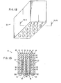
- FIG. 12 shows a multilayered
ceramic capacitor 70 which employs a matrix of holes into which high dielectric constant material is inserted to provide high capacitance. Thin layers of metal serving as electrodes are deposited upon the interfaces between layers of ceramic material as the capacitor is being assembled.Solder balls capacitor 70 is adapted for attachment to the upper surface of a chip carrier such ascarrier 12 or even aninterposer 10 in FIG. 2. FIG. 13 shows a sectional view of the capacitor of FIG. 12 taken along line FIG. 13- FIG. 13 in FIG. 12. Thesolder balls ball 96 iselectrode 90 which is designated - to indicate polarity. Connected tosolder ball 97 which is designated + to indicate positive electrical polarity is a pair ofcapacitor plates ceramic layer 83. Theplates ceramic material 80, 81 (carrying plate 90) layer 82 (perforated and containing dielectric discs 22), withplate 91 next, thenceramic layer 83 followed byplate 92, ceramic layer 84 (perforated and containing dielectric discs 22), negative plate layer 93 (connected to negative solder ball 98),ceramic layer 85, plate layer 94 (connected tosolder ball 98 also). Next ceramic layer 86 (perforated and containing dielectric discs 22) is betweenplate 94 andplate 95.Plate 95 is connected topositive solder ball 99. The next ceramic layer islayer 87 laminated to plate 95, and the last ceramic layer islayer 88. On the lower ends of the plates 90-95 there are extensions as can be seen by reference to FIG. 14 wherein the extension ofplate 90 istab 101, and the extensions ofplates tabs plates disc 100 which bridges the space betweentabs Additional discs 100 are shown in FIG. 13 for the purpose of connectingplate 90 tosolder ball 96,plate 93 andplate 94 tosolder ball 98 and for connectingplate electrode 95 tosolder ball 99. - In a modification of FIG. 13,
disc 100 can be extended across to join several sets of capacitor plates if the tabs extending therefrom are staggered. - In FIG. 14 the locations of the solder balls are not exploded as much as shown by the
ellipses solder balls capacitor plate several tabs discs 100 and the solder balls shown in FIG. 12. FIG. 14 gives a better view of the sides of theindividual layers - When a capacitor composed of
plates electrode 97 rises in potential current will be flowing up into bothplates plates
Claims (8)
Applications Claiming Priority (2)
| Application Number | Priority Date | Filing Date | Title |
|---|---|---|---|
| US176949 | 1980-08-11 | ||
| US06/176,949 US4349862A (en) | 1980-08-11 | 1980-08-11 | Capacitive chip carrier and multilayer ceramic capacitors |
Publications (2)
| Publication Number | Publication Date |
|---|---|
| EP0045877A1 true EP0045877A1 (en) | 1982-02-17 |
| EP0045877B1 EP0045877B1 (en) | 1984-10-31 |
Family
ID=22646554
Family Applications (1)
| Application Number | Title | Priority Date | Filing Date |
|---|---|---|---|
| EP81105736A Expired EP0045877B1 (en) | 1980-08-11 | 1981-07-21 | Laminated ceramic sheet printed circuit components including capacitance means |
Country Status (4)
| Country | Link |
|---|---|
| US (1) | US4349862A (en) |
| EP (1) | EP0045877B1 (en) |
| JP (1) | JPS5737818A (en) |
| DE (1) | DE3166953D1 (en) |
Cited By (16)
| Publication number | Priority date | Publication date | Assignee | Title |
|---|---|---|---|---|
| EP0111890A2 (en) * | 1982-12-15 | 1984-06-27 | Nec Corporation | Monolithic multicomponents ceramic substrate with at least one dielectric layer of a composition having a Perovskite structure |
| FR2556503A1 (en) * | 1983-12-08 | 1985-06-14 | Eurofarad | ALUMINA INTERCONNECTION SUBSTRATE FOR ELECTRONIC COMPONENT |
| US4714952A (en) * | 1984-11-01 | 1987-12-22 | Nec Corporation | Capacitor built-in integrated circuit packaged unit and process of fabrication thereof |
| EP0337686A2 (en) * | 1988-04-12 | 1989-10-18 | Hitachi, Ltd. | Semiconductor chip module |
| US5049979A (en) * | 1990-06-18 | 1991-09-17 | Microelectronics And Computer Technology Corporation | Combined flat capacitor and tab integrated circuit chip and method |
| EP0451500A2 (en) * | 1990-04-09 | 1991-10-16 | International Business Machines Corporation | Printed circuit boards and cards having buried thin film capacitors and processing techniques for fabricating said boards and cards |
| EP0491542A1 (en) * | 1990-12-17 | 1992-06-24 | Hughes Aircraft Company | Via capacitors within multi-layer 3-dimensional structures/substrates |
| WO1992022994A1 (en) * | 1991-06-14 | 1992-12-23 | Telefonaktiebolaget Lm Ericsson | A device comprising laminated conductive patterns and easily selectable dielectrics |
| EP0526707A1 (en) * | 1991-08-05 | 1993-02-10 | Hughes Aircraft Company | Low temperature co-fired ceramic structure containing buried capacitors |
| US5219787A (en) * | 1990-07-23 | 1993-06-15 | Microelectronics And Computer Technology Corporation | Trenching techniques for forming channels, vias and components in substrates |
| EP0574206A2 (en) * | 1992-06-08 | 1993-12-15 | Nippon CMK Corp. | Multilayer printed circuit board and method for manufacturing the same |
| US5272600A (en) * | 1992-09-02 | 1993-12-21 | Microelectronics And Computer Technology Corporation | Electrical interconnect device with interwoven power and ground lines and capacitive vias |
| EP0581712A2 (en) * | 1992-07-29 | 1994-02-02 | International Business Machines Corporation | MLC conductor pattern off-set design to eliminate line to via cracking |
| WO1994023554A1 (en) * | 1993-04-07 | 1994-10-13 | Zycon Corporation | Annular circuit components coupled with printed circuit board through-hole |
| WO2015048708A1 (en) * | 2013-09-30 | 2015-04-02 | Anaren, Inc. | High power rf circuit |
| EP4199070A1 (en) * | 2021-12-16 | 2023-06-21 | INTEL Corporation | Coupled fins with blind trench structures |
Families Citing this family (92)
| Publication number | Priority date | Publication date | Assignee | Title |
|---|---|---|---|---|
| JPS5842262A (en) * | 1981-09-07 | 1983-03-11 | Toshiba Corp | Connection of lead wire for hybrid integrated circuit |
| US4791391A (en) * | 1983-03-30 | 1988-12-13 | E. I. Du Pont De Nemours And Company | Planar filter connector having thick film capacitors |
| US4616290A (en) * | 1983-04-19 | 1986-10-07 | Murata Manufacturing Co., Ltd. | Electric double layer capacitor |
| US4598470A (en) * | 1983-06-20 | 1986-07-08 | International Business Machines Corporation | Method for providing improved electrical and mechanical connection between I/O pin and transverse via substrate |
| US4727410A (en) * | 1983-11-23 | 1988-02-23 | Cabot Technical Ceramics, Inc. | High density integrated circuit package |
| US4617730A (en) * | 1984-08-13 | 1986-10-21 | International Business Machines Corporation | Method of fabricating a chip interposer |
| US4652977A (en) * | 1984-09-13 | 1987-03-24 | Schlumberger Technology Corporation | Microelectronics module |
| US4705606A (en) * | 1985-01-31 | 1987-11-10 | Gould Inc. | Thin-film electrical connections for integrated circuits |
| US4996584A (en) * | 1985-01-31 | 1991-02-26 | Gould, Inc. | Thin-film electrical connections for integrated circuits |
| US4731699A (en) * | 1985-10-08 | 1988-03-15 | Nec Corporation | Mounting structure for a chip |
| US4700473A (en) * | 1986-01-03 | 1987-10-20 | Motorola Inc. | Method of making an ultra high density pad array chip carrier |
| US4945399A (en) * | 1986-09-30 | 1990-07-31 | International Business Machines Corporation | Electronic package with integrated distributed decoupling capacitors |
| GB2197540B (en) * | 1986-11-12 | 1991-04-17 | Murata Manufacturing Co | A circuit structure. |
| US4803595A (en) * | 1986-11-17 | 1989-02-07 | International Business Machines Corporation | Interposer chip technique for making engineering changes between interconnected semiconductor chips |
| US4744008A (en) * | 1986-11-18 | 1988-05-10 | International Business Machines Corporation | Flexible film chip carrier with decoupling capacitors |
| US4858077A (en) * | 1987-11-25 | 1989-08-15 | Hitachi, Ltd. | Condenser-containing, ceramic multi-layer circuit board and semiconductor module and computer having the circuit board |
| US4864465A (en) * | 1988-05-10 | 1989-09-05 | The United States Of America | Viad chip capacitor and method for making same |
| US6124625A (en) * | 1988-05-31 | 2000-09-26 | Micron Technology, Inc. | Chip decoupling capacitor |
| US5687109A (en) * | 1988-05-31 | 1997-11-11 | Micron Technology, Inc. | Integrated circuit module having on-chip surge capacitors |
| US4831494A (en) * | 1988-06-27 | 1989-05-16 | International Business Machines Corporation | Multilayer capacitor |
| USRE35064E (en) * | 1988-08-01 | 1995-10-17 | Circuit Components, Incorporated | Multilayer printed wiring board |
| JP2776909B2 (en) * | 1988-09-14 | 1998-07-16 | 株式会社日立製作所 | Carrier board |
| CA2002213C (en) * | 1988-11-10 | 1999-03-30 | Iwona Turlik | High performance integrated circuit chip package and method of making same |
| US5056216A (en) * | 1990-01-26 | 1991-10-15 | Sri International | Method of forming a plurality of solder connections |
| US5357403A (en) * | 1990-06-29 | 1994-10-18 | General Electric Company | Adaptive lithography in a high density interconnect structure whose signal layers have fixed patterns |
| US5148265A (en) | 1990-09-24 | 1992-09-15 | Ist Associates, Inc. | Semiconductor chip assemblies with fan-in leads |
| US5148266A (en) * | 1990-09-24 | 1992-09-15 | Ist Associates, Inc. | Semiconductor chip assemblies having interposer and flexible lead |
| US7198969B1 (en) | 1990-09-24 | 2007-04-03 | Tessera, Inc. | Semiconductor chip assemblies, methods of making same and components for same |
| US5679977A (en) * | 1990-09-24 | 1997-10-21 | Tessera, Inc. | Semiconductor chip assemblies, methods of making same and components for same |
| US5254493A (en) * | 1990-10-30 | 1993-10-19 | Microelectronics And Computer Technology Corporation | Method of fabricating integrated resistors in high density substrates |
| US5120572A (en) * | 1990-10-30 | 1992-06-09 | Microelectronics And Computer Technology Corporation | Method of fabricating electrical components in high density substrates |
| US5132613A (en) * | 1990-11-30 | 1992-07-21 | International Business Machines Corporation | Low inductance side mount decoupling test structure |
| US5177594A (en) * | 1991-01-09 | 1993-01-05 | International Business Machines Corporation | Semiconductor chip interposer module with engineering change wiring and distributed decoupling capacitance |
| US5177670A (en) * | 1991-02-08 | 1993-01-05 | Hitachi, Ltd. | Capacitor-carrying semiconductor module |
| US5379191A (en) * | 1991-02-26 | 1995-01-03 | Microelectronics And Computer Technology Corporation | Compact adapter package providing peripheral to area translation for an integrated circuit chip |
| US5749049A (en) * | 1991-11-01 | 1998-05-05 | Worp; Nicholas Jacob | Method and apparatus for measuring the inherent capacitance of a circuit supporting substrate |
| JP2772184B2 (en) * | 1991-11-07 | 1998-07-02 | 株式会社東芝 | Semiconductor device |
| US5339212A (en) * | 1992-12-03 | 1994-08-16 | International Business Machines Corporation | Sidewall decoupling capacitor |
| US6728113B1 (en) * | 1993-06-24 | 2004-04-27 | Polychip, Inc. | Method and apparatus for non-conductively interconnecting integrated circuits |
| JP3461204B2 (en) | 1993-09-14 | 2003-10-27 | 株式会社東芝 | Multi-chip module |
| US5530288A (en) * | 1994-10-12 | 1996-06-25 | International Business Machines Corporation | Passive interposer including at least one passive electronic component |
| US6000126A (en) * | 1996-03-29 | 1999-12-14 | General Dynamics Information Systems, Inc. | Method and apparatus for connecting area grid arrays to printed wire board |
| US5764485A (en) * | 1996-04-19 | 1998-06-09 | Lebaschi; Ali | Multi-layer PCB blockade-via pad-connection |
| DE19638195A1 (en) * | 1996-09-19 | 1998-04-02 | Bosch Gmbh Robert | Lead-free dielectric paste |
| US7321485B2 (en) | 1997-04-08 | 2008-01-22 | X2Y Attenuators, Llc | Arrangement for energy conditioning |
| US7336468B2 (en) | 1997-04-08 | 2008-02-26 | X2Y Attenuators, Llc | Arrangement for energy conditioning |
| US9054094B2 (en) | 1997-04-08 | 2015-06-09 | X2Y Attenuators, Llc | Energy conditioning circuit arrangement for integrated circuit |
| JP4032459B2 (en) * | 1997-08-05 | 2008-01-16 | 株式会社デンソー | Hybrid integrated circuit substrate and method of manufacturing the same |
| US6005197A (en) * | 1997-08-25 | 1999-12-21 | Lucent Technologies Inc. | Embedded thin film passive components |
| CN1257053C (en) * | 1997-11-18 | 2006-05-24 | 松下电器产业株式会社 | Stacked body and capacitor |
| US5973391A (en) * | 1997-12-11 | 1999-10-26 | Read-Rite Corporation | Interposer with embedded circuitry and method for using the same to package microelectronic units |
| US6072690A (en) * | 1998-01-15 | 2000-06-06 | International Business Machines Corporation | High k dielectric capacitor with low k sheathed signal vias |
| US6178082B1 (en) * | 1998-02-26 | 2001-01-23 | International Business Machines Corporation | High temperature, conductive thin film diffusion barrier for ceramic/metal systems |
| US6114756A (en) | 1998-04-01 | 2000-09-05 | Micron Technology, Inc. | Interdigitated capacitor design for integrated circuit leadframes |
| US6414391B1 (en) * | 1998-06-30 | 2002-07-02 | Micron Technology, Inc. | Module assembly for stacked BGA packages with a common bus bar in the assembly |
| US5973928A (en) * | 1998-08-18 | 1999-10-26 | International Business Machines Corporation | Multi-layer ceramic substrate decoupling |
| TW395601U (en) * | 1998-08-20 | 2000-06-21 | Hon Hai Prec Ind Co Ltd | Connector with BGA arrangement for connecting to pc board |
| US6274937B1 (en) * | 1999-02-01 | 2001-08-14 | Micron Technology, Inc. | Silicon multi-chip module packaging with integrated passive components and method of making |
| US6617681B1 (en) * | 1999-06-28 | 2003-09-09 | Intel Corporation | Interposer and method of making same |
| TW512653B (en) * | 1999-11-26 | 2002-12-01 | Ibiden Co Ltd | Multilayer circuit board and semiconductor device |
| JP2001185442A (en) * | 1999-12-27 | 2001-07-06 | Murata Mfg Co Ltd | Connection structure of multiplayer capacitor and decoupling capacitor and wiring substrate |
| US6351391B1 (en) | 2000-05-15 | 2002-02-26 | International Business Machines Corporation | Signal busses on printed board structures mounting ASIC chips with signal termination resistor devices using planar signal terminating devices |
| US6407929B1 (en) * | 2000-06-29 | 2002-06-18 | Intel Corporation | Electronic package having embedded capacitors and method of fabrication therefor |
| US6399892B1 (en) | 2000-09-19 | 2002-06-04 | International Business Machines Corporation | CTE compensated chip interposer |
| US6388207B1 (en) | 2000-12-29 | 2002-05-14 | Intel Corporation | Electronic assembly with trench structures and methods of manufacture |
| US6477032B2 (en) * | 2001-01-31 | 2002-11-05 | Avx Corporation | Low inductance chip with center via contact |
| US6729019B2 (en) * | 2001-07-11 | 2004-05-04 | Formfactor, Inc. | Method of manufacturing a probe card |
| US6963493B2 (en) * | 2001-11-08 | 2005-11-08 | Avx Corporation | Multilayer electronic devices with via components |
| US6768650B2 (en) * | 2002-02-07 | 2004-07-27 | International Business Machines Corporation | Method and structure for reduction of impedance using decoupling capacitor |
| JP3678212B2 (en) * | 2002-05-20 | 2005-08-03 | ウシオ電機株式会社 | Super high pressure mercury lamp |
| US6791133B2 (en) * | 2002-07-19 | 2004-09-14 | International Business Machines Corporation | Interposer capacitor built on silicon wafer and joined to a ceramic substrate |
| US6755700B2 (en) * | 2002-11-12 | 2004-06-29 | Modevation Enterprises Inc. | Reset speed control for watercraft |
| US6806563B2 (en) * | 2003-03-20 | 2004-10-19 | International Business Machines Corporation | Composite capacitor and stiffener for chip carrier |
| TWI236124B (en) * | 2004-06-30 | 2005-07-11 | Airoha Tech Corp | Multilayer leadframe module with embedded passive components and method of producing the same |
| US7348661B2 (en) * | 2004-09-24 | 2008-03-25 | Intel Corporation | Array capacitor apparatuses to filter input/output signal |
| US7425760B1 (en) | 2004-10-13 | 2008-09-16 | Sun Microsystems, Inc. | Multi-chip module structure with power delivery using flexible cables |
| US7426780B2 (en) * | 2004-11-10 | 2008-09-23 | Enpirion, Inc. | Method of manufacturing a power module |
| JP4499548B2 (en) * | 2004-12-24 | 2010-07-07 | 新光電気工業株式会社 | Capacitor parts |
| JP2008535207A (en) | 2005-03-01 | 2008-08-28 | エックストゥーワイ アテニュエイターズ,エルエルシー | Regulator with coplanar conductor |
| US7435627B2 (en) * | 2005-08-11 | 2008-10-14 | International Business Machines Corporation | Techniques for providing decoupling capacitance |
| US8631560B2 (en) | 2005-10-05 | 2014-01-21 | Enpirion, Inc. | Method of forming a magnetic device having a conductive clip |
| US7688172B2 (en) | 2005-10-05 | 2010-03-30 | Enpirion, Inc. | Magnetic device having a conductive clip |
| US20100044089A1 (en) * | 2007-03-01 | 2010-02-25 | Akinobu Shibuya | Interposer integrated with capacitors and method for manufacturing the same |
| US8476735B2 (en) * | 2007-05-29 | 2013-07-02 | Taiwan Semiconductor Manufacturing Company, Ltd. | Programmable semiconductor interposer for electronic package and method of forming |
| US7920042B2 (en) | 2007-09-10 | 2011-04-05 | Enpirion, Inc. | Micromagnetic device and method of forming the same |
| US8266793B2 (en) * | 2008-10-02 | 2012-09-18 | Enpirion, Inc. | Module having a stacked magnetic device and semiconductor device and method of forming the same |
| US9054086B2 (en) | 2008-10-02 | 2015-06-09 | Enpirion, Inc. | Module having a stacked passive element and method of forming the same |
| US8339802B2 (en) | 2008-10-02 | 2012-12-25 | Enpirion, Inc. | Module having a stacked magnetic device and semiconductor device and method of forming the same |
| US8760847B2 (en) | 2010-11-30 | 2014-06-24 | Pratt & Whitney Canada Corp. | Low inductance capacitor assembly |
| US9852941B2 (en) | 2014-10-03 | 2017-12-26 | Analog Devices, Inc. | Stacked conductor structure and methods for manufacture of same |
| US10084310B1 (en) * | 2016-02-08 | 2018-09-25 | National Technology & Engineering Solutions Of Sandia, Llc | Low-inductance direct current power bus |
| US11071213B2 (en) * | 2019-07-24 | 2021-07-20 | The Boeing Company | Methods of manufacturing a high impedance surface (HIS) enhanced by discrete passives |
Citations (2)
| Publication number | Priority date | Publication date | Assignee | Title |
|---|---|---|---|---|
| US2913632A (en) * | 1955-08-08 | 1959-11-17 | Austin N Stanton | Micro-circuits, electric devices there-for, and methods for making same |
| DE2546400A1 (en) * | 1975-10-16 | 1977-04-21 | Siemens Ag | RC network for mass prodn. - consists of RC layers and contact pads on pastic foil base with thick thermoplastic covering |
Family Cites Families (9)
| Publication number | Priority date | Publication date | Assignee | Title |
|---|---|---|---|---|
| GB856584A (en) * | 1956-03-20 | 1960-12-21 | Barton Lee Weller | Improvements in or relating to composite electrical components and methods of manufacturing same |
| US3273033A (en) * | 1963-08-29 | 1966-09-13 | Litton Systems Inc | Multidielectric thin film capacitors |
| US4109377A (en) * | 1976-02-03 | 1978-08-29 | International Business Machines Corporation | Method for preparing a multilayer ceramic |
| US4202007A (en) * | 1978-06-23 | 1980-05-06 | International Business Machines Corporation | Multi-layer dielectric planar structure having an internal conductor pattern characterized with opposite terminations disposed at a common edge surface of the layers |
| US4249196A (en) * | 1978-08-21 | 1981-02-03 | Burroughs Corporation | Integrated circuit module with integral capacitor |
| US4210950A (en) * | 1978-09-29 | 1980-07-01 | Bell Telephone Laboratories, Incorporated | High-ratio-accuracy capacitor geometries for integrated circuits |
| US4247881A (en) * | 1979-04-02 | 1981-01-27 | Sprague Electric Company | Discoidal monolithic ceramic capacitor |
| US4237522A (en) * | 1979-06-29 | 1980-12-02 | International Business Machines Corporation | Chip package with high capacitance, stacked vlsi/power sheets extending through slots in substrate |
| US4274124A (en) * | 1979-12-26 | 1981-06-16 | International Business Machines Corporation | Thick film capacitor having very low internal inductance |
-
1980
- 1980-08-11 US US06/176,949 patent/US4349862A/en not_active Expired - Lifetime
-
1981
- 1981-06-12 JP JP8977081A patent/JPS5737818A/en active Granted
- 1981-07-21 DE DE8181105736T patent/DE3166953D1/en not_active Expired
- 1981-07-21 EP EP81105736A patent/EP0045877B1/en not_active Expired
Patent Citations (2)
| Publication number | Priority date | Publication date | Assignee | Title |
|---|---|---|---|---|
| US2913632A (en) * | 1955-08-08 | 1959-11-17 | Austin N Stanton | Micro-circuits, electric devices there-for, and methods for making same |
| DE2546400A1 (en) * | 1975-10-16 | 1977-04-21 | Siemens Ag | RC network for mass prodn. - consists of RC layers and contact pads on pastic foil base with thick thermoplastic covering |
Non-Patent Citations (1)
| Title |
|---|
| IBM Technical Disclosure Bulletin, Vol. 22, No. 5, October 1979 New York A.H. JOHNSON et al. "Multilayer Ceramic Fixed Layer Substrate Design" pages 1841, 1842 *paragraphs 1 to 4; fig.* * |
Cited By (24)
| Publication number | Priority date | Publication date | Assignee | Title |
|---|---|---|---|---|
| EP0111890A2 (en) * | 1982-12-15 | 1984-06-27 | Nec Corporation | Monolithic multicomponents ceramic substrate with at least one dielectric layer of a composition having a Perovskite structure |
| EP0111890A3 (en) * | 1982-12-15 | 1986-12-30 | Nec Corporation | Monolithic multicomponents ceramic substrate with at least one dielectric layer of a composition having a perovskite structure |
| FR2556503A1 (en) * | 1983-12-08 | 1985-06-14 | Eurofarad | ALUMINA INTERCONNECTION SUBSTRATE FOR ELECTRONIC COMPONENT |
| EP0145599A2 (en) * | 1983-12-08 | 1985-06-19 | Eurofarad Efd | Alumina interconnection substrate for an electronic component, and method for its production |
| EP0145599A3 (en) * | 1983-12-08 | 1985-07-10 | Eurofarad Efd | Alumina interconnection substrate for an electronic component, and method for its production |
| US4714952A (en) * | 1984-11-01 | 1987-12-22 | Nec Corporation | Capacitor built-in integrated circuit packaged unit and process of fabrication thereof |
| EP0337686A2 (en) * | 1988-04-12 | 1989-10-18 | Hitachi, Ltd. | Semiconductor chip module |
| EP0337686A3 (en) * | 1988-04-12 | 1991-05-22 | Hitachi, Ltd. | Semiconductor chip module |
| EP0451500A2 (en) * | 1990-04-09 | 1991-10-16 | International Business Machines Corporation | Printed circuit boards and cards having buried thin film capacitors and processing techniques for fabricating said boards and cards |
| EP0451500A3 (en) * | 1990-04-09 | 1995-02-08 | Ibm | |
| US5049979A (en) * | 1990-06-18 | 1991-09-17 | Microelectronics And Computer Technology Corporation | Combined flat capacitor and tab integrated circuit chip and method |
| US5219787A (en) * | 1990-07-23 | 1993-06-15 | Microelectronics And Computer Technology Corporation | Trenching techniques for forming channels, vias and components in substrates |
| EP0491542A1 (en) * | 1990-12-17 | 1992-06-24 | Hughes Aircraft Company | Via capacitors within multi-layer 3-dimensional structures/substrates |
| WO1992022994A1 (en) * | 1991-06-14 | 1992-12-23 | Telefonaktiebolaget Lm Ericsson | A device comprising laminated conductive patterns and easily selectable dielectrics |
| US5319330A (en) * | 1991-06-14 | 1994-06-07 | Telefonaktiebolaget L M Ericsson | Device comprising laminated conductive patterns and easily selectable dielectrics |
| EP0526707A1 (en) * | 1991-08-05 | 1993-02-10 | Hughes Aircraft Company | Low temperature co-fired ceramic structure containing buried capacitors |
| EP0574206A3 (en) * | 1992-06-08 | 1994-01-12 | Nippon CMK Corp. | Multilayer printed circuit board and method for manufacturing the same |
| EP0574206A2 (en) * | 1992-06-08 | 1993-12-15 | Nippon CMK Corp. | Multilayer printed circuit board and method for manufacturing the same |
| EP0581712A2 (en) * | 1992-07-29 | 1994-02-02 | International Business Machines Corporation | MLC conductor pattern off-set design to eliminate line to via cracking |
| EP0581712A3 (en) * | 1992-07-29 | 1994-04-06 | Ibm | |
| US5272600A (en) * | 1992-09-02 | 1993-12-21 | Microelectronics And Computer Technology Corporation | Electrical interconnect device with interwoven power and ground lines and capacitive vias |
| WO1994023554A1 (en) * | 1993-04-07 | 1994-10-13 | Zycon Corporation | Annular circuit components coupled with printed circuit board through-hole |
| WO2015048708A1 (en) * | 2013-09-30 | 2015-04-02 | Anaren, Inc. | High power rf circuit |
| EP4199070A1 (en) * | 2021-12-16 | 2023-06-21 | INTEL Corporation | Coupled fins with blind trench structures |
Also Published As
| Publication number | Publication date |
|---|---|
| JPS5737818A (en) | 1982-03-02 |
| JPS6348172B2 (en) | 1988-09-28 |
| DE3166953D1 (en) | 1984-12-06 |
| EP0045877B1 (en) | 1984-10-31 |
| US4349862A (en) | 1982-09-14 |
Similar Documents
| Publication | Publication Date | Title |
|---|---|---|
| EP0045877B1 (en) | Laminated ceramic sheet printed circuit components including capacitance means | |
| US4202007A (en) | Multi-layer dielectric planar structure having an internal conductor pattern characterized with opposite terminations disposed at a common edge surface of the layers | |
| EP0100175B1 (en) | Chip capacitor having a compliant termination | |
| EP0042987B1 (en) | Electronic circuit chip carrier | |
| US6072690A (en) | High k dielectric capacitor with low k sheathed signal vias | |
| US4645552A (en) | Process for fabricating dimensionally stable interconnect boards | |
| US4648179A (en) | Process of making interconnection structure for semiconductor device | |
| US3549784A (en) | Ceramic-metallic composite substrate | |
| JPS63132415A (en) | Decoupling capacitor for pin-grid array package | |
| CN1159249A (en) | Improvements in ceramic chip fuses | |
| US4910643A (en) | Thick film, multi-layer, ceramic interconnected circuit board | |
| US4193082A (en) | Multi-layer dielectric structure | |
| US5625528A (en) | Monolithic, buried-substrate, ceramic multiple capacitors isolated, one to the next, by dual-dielectric-constant, three-layer-laminate isolation layers | |
| US8541694B2 (en) | Multilayer wiring board | |
| US5740010A (en) | Printing and adhering patterned metal on laid-up multi-layer green wafer before firing so as to later form precise integral co-fired conductive traces and pads on top and bottom surfaces of monolithic, buried-substrate, capacitors | |
| US5655209A (en) | Multilayer ceramic substrates having internal capacitor, and process for producing same | |
| US4652977A (en) | Microelectronics module | |
| US6676784B2 (en) | Process for the manufacture of multilayer ceramic substrates | |
| JPH05299291A (en) | High dielectric-const. flexible sheet, multilayer circuit board having the same, bus bar and multilayer capacitor | |
| US6011684A (en) | Monolithic integrated multiple electronic components internally interconnected and externally connected by conductive side castellations to the monolith that are of varying width particularly monolithic multiple capacitors | |
| JP3084209B2 (en) | Electronic component and manufacturing method thereof | |
| EP0359513A2 (en) | Semiconductor chip carrier and method of making it | |
| JPH0754778B2 (en) | Ceramic board with built-in capacitor | |
| JPH05347227A (en) | Laminated thin film capacitor | |
| JP3909285B2 (en) | Wiring board |
Legal Events
| Date | Code | Title | Description |
|---|---|---|---|
| PUAI | Public reference made under article 153(3) epc to a published international application that has entered the european phase |
Free format text: ORIGINAL CODE: 0009012 |
|
| AK | Designated contracting states |
Designated state(s): DE FR GB IT |
|
| 17P | Request for examination filed |
Effective date: 19820309 |
|
| ITF | It: translation for a ep patent filed |
Owner name: IBM - DR. ALFREDO BRAVI |
|
| GRAA | (expected) grant |
Free format text: ORIGINAL CODE: 0009210 |
|
| AK | Designated contracting states |
Designated state(s): DE FR GB IT |
|
| REF | Corresponds to: |
Ref document number: 3166953 Country of ref document: DE Date of ref document: 19841206 |
|
| ET | Fr: translation filed | ||
| PLBE | No opposition filed within time limit |
Free format text: ORIGINAL CODE: 0009261 |
|
| STAA | Information on the status of an ep patent application or granted ep patent |
Free format text: STATUS: NO OPPOSITION FILED WITHIN TIME LIMIT |
|
| 26N | No opposition filed | ||
| ITTA | It: last paid annual fee | ||
| PGFP | Annual fee paid to national office [announced via postgrant information from national office to epo] |
Ref country code: FR Payment date: 19960704 Year of fee payment: 16 |
|
| PGFP | Annual fee paid to national office [announced via postgrant information from national office to epo] |
Ref country code: GB Payment date: 19970625 Year of fee payment: 17 |
|
| PG25 | Lapsed in a contracting state [announced via postgrant information from national office to epo] |
Ref country code: FR Free format text: LAPSE BECAUSE OF NON-PAYMENT OF DUE FEES Effective date: 19980331 |
|
| REG | Reference to a national code |
Ref country code: FR Ref legal event code: ST |
|
| PG25 | Lapsed in a contracting state [announced via postgrant information from national office to epo] |
Ref country code: GB Free format text: LAPSE BECAUSE OF NON-PAYMENT OF DUE FEES Effective date: 19980721 |
|
| GBPC | Gb: european patent ceased through non-payment of renewal fee |
Effective date: 19980721 |
|
| PGFP | Annual fee paid to national office [announced via postgrant information from national office to epo] |
Ref country code: DE Payment date: 19990715 Year of fee payment: 19 |
|
| PG25 | Lapsed in a contracting state [announced via postgrant information from national office to epo] |
Ref country code: DE Free format text: LAPSE BECAUSE OF NON-PAYMENT OF DUE FEES Effective date: 20010501 |