EP0035299B1 - Display device - Google Patents
Display device Download PDFInfo
- Publication number
- EP0035299B1 EP0035299B1 EP81200186A EP81200186A EP0035299B1 EP 0035299 B1 EP0035299 B1 EP 0035299B1 EP 81200186 A EP81200186 A EP 81200186A EP 81200186 A EP81200186 A EP 81200186A EP 0035299 B1 EP0035299 B1 EP 0035299B1
- Authority
- EP
- European Patent Office
- Prior art keywords
- layer
- electrodes
- display device
- supporting plate
- electrode
- Prior art date
- Legal status (The legal status is an assumption and is not a legal conclusion. Google has not performed a legal analysis and makes no representation as to the accuracy of the status listed.)
- Expired
Links
- 229910052782 aluminium Inorganic materials 0.000 claims description 24
- 239000004411 aluminium Substances 0.000 claims description 24
- XAGFODPZIPBFFR-UHFFFAOYSA-N aluminium Chemical compound [Al] XAGFODPZIPBFFR-UHFFFAOYSA-N 0.000 claims description 24
- 239000007772 electrode material Substances 0.000 claims description 13
- 238000010894 electron beam technology Methods 0.000 claims description 12
- 238000000034 method Methods 0.000 claims description 11
- 239000011521 glass Substances 0.000 claims description 9
- 238000004519 manufacturing process Methods 0.000 claims description 9
- 230000003287 optical effect Effects 0.000 claims description 9
- 238000001259 photo etching Methods 0.000 claims description 7
- 230000001419 dependent effect Effects 0.000 claims description 6
- 238000000151 deposition Methods 0.000 claims description 4
- 239000000463 material Substances 0.000 claims description 4
- 238000007743 anodising Methods 0.000 claims description 2
- 230000003014 reinforcing effect Effects 0.000 claims description 2
- PXHVJJICTQNCMI-UHFFFAOYSA-N Nickel Chemical compound [Ni] PXHVJJICTQNCMI-UHFFFAOYSA-N 0.000 description 17
- 229910052759 nickel Inorganic materials 0.000 description 9
- 238000006073 displacement reaction Methods 0.000 description 4
- PNEYBMLMFCGWSK-UHFFFAOYSA-N Alumina Chemical compound [O-2].[O-2].[O-2].[Al+3].[Al+3] PNEYBMLMFCGWSK-UHFFFAOYSA-N 0.000 description 3
- VYZAMTAEIAYCRO-UHFFFAOYSA-N Chromium Chemical compound [Cr] VYZAMTAEIAYCRO-UHFFFAOYSA-N 0.000 description 3
- 229910052804 chromium Inorganic materials 0.000 description 3
- 239000011651 chromium Substances 0.000 description 3
- 238000010276 construction Methods 0.000 description 3
- 230000000694 effects Effects 0.000 description 3
- 238000009713 electroplating Methods 0.000 description 3
- 239000013078 crystal Substances 0.000 description 2
- 239000011159 matrix material Substances 0.000 description 2
- GRYLNZFGIOXLOG-UHFFFAOYSA-N Nitric acid Chemical group O[N+]([O-])=O GRYLNZFGIOXLOG-UHFFFAOYSA-N 0.000 description 1
- HJSXWIZOWRQPPY-UHFFFAOYSA-N O=S=O.O=S=O.[Ni+2] Chemical compound O=S=O.O=S=O.[Ni+2] HJSXWIZOWRQPPY-UHFFFAOYSA-N 0.000 description 1
- 239000003086 colorant Substances 0.000 description 1
- 230000003247 decreasing effect Effects 0.000 description 1
- 238000004070 electrodeposition Methods 0.000 description 1
- 238000005530 etching Methods 0.000 description 1
- 229910003437 indium oxide Inorganic materials 0.000 description 1
- PJXISJQVUVHSOJ-UHFFFAOYSA-N indium(iii) oxide Chemical compound [O-2].[O-2].[O-2].[In+3].[In+3] PJXISJQVUVHSOJ-UHFFFAOYSA-N 0.000 description 1
- 239000011810 insulating material Substances 0.000 description 1
- 239000007788 liquid Substances 0.000 description 1
- 229910017604 nitric acid Inorganic materials 0.000 description 1
- 230000002787 reinforcement Effects 0.000 description 1
- 229910052709 silver Inorganic materials 0.000 description 1
- 238000001228 spectrum Methods 0.000 description 1
- XOLBLPGZBRYERU-UHFFFAOYSA-N tin dioxide Chemical compound O=[Sn]=O XOLBLPGZBRYERU-UHFFFAOYSA-N 0.000 description 1
- 229910001887 tin oxide Inorganic materials 0.000 description 1
Images


Classifications
-
- G—PHYSICS
- G09—EDUCATION; CRYPTOGRAPHY; DISPLAY; ADVERTISING; SEALS
- G09F—DISPLAYING; ADVERTISING; SIGNS; LABELS OR NAME-PLATES; SEALS
- G09F9/00—Indicating arrangements for variable information in which the information is built-up on a support by selection or combination of individual elements
- G09F9/30—Indicating arrangements for variable information in which the information is built-up on a support by selection or combination of individual elements in which the desired character or characters are formed by combining individual elements
- G09F9/37—Indicating arrangements for variable information in which the information is built-up on a support by selection or combination of individual elements in which the desired character or characters are formed by combining individual elements being movable elements
- G09F9/372—Indicating arrangements for variable information in which the information is built-up on a support by selection or combination of individual elements in which the desired character or characters are formed by combining individual elements being movable elements the positions of the elements being controlled by the application of an electric field
-
- G—PHYSICS
- G02—OPTICS
- G02B—OPTICAL ELEMENTS, SYSTEMS OR APPARATUS
- G02B26/00—Optical devices or arrangements for the control of light using movable or deformable optical elements
- G02B26/001—Optical devices or arrangements for the control of light using movable or deformable optical elements based on interference in an adjustable optical cavity
-
- G—PHYSICS
- G02—OPTICS
- G02F—OPTICAL DEVICES OR ARRANGEMENTS FOR THE CONTROL OF LIGHT BY MODIFICATION OF THE OPTICAL PROPERTIES OF THE MEDIA OF THE ELEMENTS INVOLVED THEREIN; NON-LINEAR OPTICS; FREQUENCY-CHANGING OF LIGHT; OPTICAL LOGIC ELEMENTS; OPTICAL ANALOGUE/DIGITAL CONVERTERS
- G02F1/00—Devices or arrangements for the control of the intensity, colour, phase, polarisation or direction of light arriving from an independent light source, e.g. switching, gating or modulating; Non-linear optics
- G02F1/01—Devices or arrangements for the control of the intensity, colour, phase, polarisation or direction of light arriving from an independent light source, e.g. switching, gating or modulating; Non-linear optics for the control of the intensity, phase, polarisation or colour
- G02F1/21—Devices or arrangements for the control of the intensity, colour, phase, polarisation or direction of light arriving from an independent light source, e.g. switching, gating or modulating; Non-linear optics for the control of the intensity, phase, polarisation or colour by interference
Definitions
- the invention relates to a display device comprising a transparent first supporting plate having a transflective layer, and a partially reflective layer which reflects to substantially the same extent as the transflective layer and which is spaced apart from the transflective layer and which is secured so as to be movable to the first supporting plate in such manner that when light is incident on the device, interference phenomena occur dependent on the distance between the transflective layer and the partially reflective layer.
- a transflective layer is meant a layer which partially transmits and partially reflects impinging light.
- the invention also relates to a method of manufacturing such a display device.
- the invention further relates to a data processing device and to a projection television device having such a display device.
- Such a display device is disclosed in United States Patent Specification 2,534,846.
- an incident light beam is partly reflected and partly transmitted by the reflective layer after which the transmitted light is partly reflected by the partially reflective layer.
- the coefficient of reflection of the transflective and partially reflective layer are approximately equal to each other so that the two layers constitute a so-called Fabry-Perot Interferometer.
- the transflective and partially reflective layers are provided on opposite sides of a piezoelectric crystal.
- the distance between the transflective and reflective layer is controlled by means of a voltage provided across the layers so that the thickness of the piezoelectric crystal varies to a greater or smaller extent.
- the construction and control of such a device are not suitable for use in a display device in which the picture is constructed from a large number of individually controllable display elements.
- a further object of the invention is to provide a display device which is suitable for displaying alphanumerical and video information.
- Still a further object of the invention is to provide a display device which can be both voltage-controlled and charge-controlled.
- Still another object of the invention is to provide a display device with which information can be observed in colour.
- a display device of a kind mentioned in the opening paragraph is characterized in that the partially reflective layer constitutes a pattern of resiliently connected electrodes and the transflective layer is divided into regions which are common for one or more resiliently connected electrodes.
- An embodiment of display device which can be constructed as a so-called cross-bar display, is characterized in that the pattern of resiliently connected electrodes constitutes a first grid of parallel strips and the common regions of the transflective layer constitute a second grid of parallel strips which cross the strips of the first grid.
- a further embodiment of a display device is characterized in that the pattern of resiliently connected electrodes constitutes a first set of electrodes and the regions of the transflective layer constitute a second set of electrodes.
- a resiliently connected electrode is attracted to an electrode of the transflective layer as a result of the electrostatic force, which movement, however, is counteracted by the resilience of the resiliently connected electrode.
- Below a given voltage dependent on the distance between the electrodes a stable equilibrium occurs between the electrostatic force and the resilience so that over a certain region of the electrode distance the distance between a resilient electrode and an electrode of the transflective layer can be adjusted.
- the equilibrium between the electrostatic force and the resilience becomes unstable so that the resiliently connected electrode is accelerated towards the electrode of the transflective layer.
- a further embodiment of a display device is characterized in that the pattern of resiliently connected electrodes constitutes a first set of electrodes and a second supporting plate which is provided with a set of electrodes which is in registration with the regions of the transflective layer is spaced apart from the first supporting plate.
- the distance between a resiliently connected electrode and a region of the transflective layer is varied by applying a voltage across an electrode of the second supporting plate and a resiliently connected electrode. Since the distance between the second supporting plate and the partially reflective layer of the resiliently connected electrodes can be chosen to be larger than the distance between the first supporting plate and the partially reflective layer of resilient electrodes, the range within which a stable equilibrium occurs between the electrostatic force and the resilience is larger than in the above-described previous embodiment. As a result of this, for controlling the observed reflection between maximum and minimum intensity, zero order effects may be used. The advantage of this is that the angle independence of the observed phenomena is large.
- the electrodes of the first set are interconnected and the electrodes of the second set are strip-shaped is characterized in that a second supporting plate is provided at some distance from the first supporting plate and has a third set of strip-shaped electrodes which cross the strip-shaped electrodes of the second set.
- the resiliently connected electrodes may engage either the first supporting plate or the second supporting plate.
- a display device having two supporting plates provided with electrodes and having resiliently connected electrodes between the supporting plates is known per se from Netherlands Patent Application 7510103. This Application, however, deals with a liquid-filled display device, while the distance between the supporting plates is much larger than the small distance between the supporting plates required for interference in a display device according to the invention.
- a display device comprises means to provide charge on the resilient electrodes.
- the control of the display device by means of charge has the advantage that throughout the distance between a resiliently connected electrode and an electrode of the transflective layer the electrostatic force occurring as a result of the charging can be in equilibrium with the resilience of a resiliently connected electrode.
- a further embodiment of a charge control display device is characterized in that the first supporting plate forms part of a glass envelope which comprises an electron gun to generate an electron beam directed onto the first supporting plate, which beam scans the first supporting plate according to a regular pattern and charges the resiliently connected electrodes.
- the resilient electrodes are provided with the desired charge by modulating the electron beam in known manner in accordance with the presented information.
- Such a display device is suitable for a data processing device which comprises a light source, first optical means to obtain a parallel light beam which is incident on the display device, which display device modulates the incident light.
- Coloured pictures can be obtained by using a light source which emits red, green and blue light.
- Such a display device is particularly suitable for a projection television device which has at least two display devices, each of which display devices comprises a light source which emits light of one colour, first optical means to obtain a parallel light beam which is incident on the display device which modulates the incident light, and second optical means to project the modulated light on a screen which is common for the display devices.
- Each display device is used to modulate light of one colour, the pictures of the display devices being projected on a screen so as to be overlapping so that a coloured picture is observed.
- a projection televison device is disclosed in United States Patent Specification 3,746,911 in which mirrors, which can be deformed, are charged by means of an electron beam. Dependent on the charge, the mirrors are curved more less. The reflected light is displayed on a screen by means of a Schlieren optical system.
- the effective part of the resilient electrodes is provided by electro deposition with a reinforcement layer of electrode material which can be etched by means of the second etchant.
- a transflective layer 1 and a partially reflective layer 2 present at a distance d therefrom.
- the coefficient of reflection of a layer 1 and layer 2 is approximately the same.
- a part of an incident light beam 3 is reflected by the transflective layer 1 and a part is transmitted.
- the transmitted light is partially reflected by the partially reflective layer 2.
- the light not reflected by the layer 2 can be transmitted or be absorbed by the layer 2.
- a number of parallel partial beams 5a, 5b and 5c are formed with decreasing intensity.
- the intensity of the reflected light as a result of the occurring interference can be controlled, by varying the distance d for a given wavelength, between substantially 0 and a maximum value which depends on the reflection coefficient of the layers 1 and 2.
- the incident light beam is composed of light of several wavelengths, reflected light of the successive wavelengths is observed when the distance d is varied.
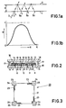
- Fig. 1 b shows the relative intensity p of the total reflected light as a function of the phase difference ⁇ determined by the distance between the layers 1 and 2, between the light reflected directly at the layer 1 and reflected at the layer 2, for a reflection coefficient of the layers 1 and 2 of 0.5.
- Fig. 2 is a diagrammatic sectional view of an embodiment of a display device.
- a plurality of strip-shaped transflective electrodes 11 are provided on a glass supporting plate 10.
- the electrodes 11 are formed by a 0.05 ⁇ m thick layer 12 of indium oxide or tin oxide on which a 0.01 to 0.02 ⁇ m thick layer 13 of chromium is provided. Instead of the layers 12 and 13, one layer only of chromium may be provided, if desired.
- Electrodes 14 are resiliently connected to pillars 1 5 at a distance of 0.3 pm from the strip-shaped electrodes 11.
- the electrodes 14 are interconnected in such manner that strip-shaped electrodes 16 are formed which are substantially at right angles to the strip-shaped electrodes 11.
- the resilient electrodes 14 are manufactured from nickel and have a thickness of 0.3 pm.
- the pillars 15 are manufactured from aluminium oxide.
- the pillars 15 may also be manufactured from the layer of nickel of the resilient electrodes themselves, which will be explained in detail with reference to Fig. 10d.
- Fig. 3 is a plan view of an individual resilient electrode 20.
- Each electrode 20 comprises a central portion 21 which via thin strips 23 is secured to the pillars 25 shown in broken lines by means of the pads 24.
- the strips 23 constitute resilient elements of the display element so that the central portion 21 of the electrodes 20 can be moved parallel to itself in a direction perpendicular to the electrodes.
- the electrode 20 has an area of 200x200 ⁇ m 2
- Fig. 4a shows diagrammatically one display element in which a transflective electrode 31 is provided on a glass supporting plate 30 and a resilient electrode 33 is provided at a distance a therefrom by means of the pillars 32.
- the resilient electrode 33 may be represented as a central reinforced portion 34 which is connected to the pads 35 by means of the springs 36 having a collective spring constant C.
- V When a voltage V is applied across the electrodes 31 and 33 the central portion 34 experiences an electrostatic force directed towards electrode 31 and an oppositely directed resilience.
- the electrode 34 is in equilibrium when it holds that: where x is the displacement of the portion 34 and ⁇ o is the permittivity of the space between electrodes 31 and 33.
- Fig. 4b the above equation is shown as a plot of V against X. For voltages below the equilibrium between the electrostatic force and the resilience is stable. For voltages above V 1 the equilibrium becomes labile and the electrode 34 flips towards electrode 31.
- the display device can be operated in various manners.
- the reflection of the incident light can be controlled from zero to maximum intensity.
- the incident light beam comprises light of various wavelengths
- reflected light of the respective wavelengths and hence colours are observed when varying the distance between the electrodes.
- the bistable mode in which the resilient electrode 34 can be only in two extreme positions.
- an embodiment slightly varied with respect to Fig. 4a is necessary as shown in Fig. 4c, in which corresponding components are referred to by the same reference numerals.
- the resilient electrode 34 flips to electrode 31.
- the electrode 31 has a number of insulating pillars 37 the height of which has been chosen to be so that when the electrode 34 engages the pillars 37 the distance between the resilient electrode 34 and electrode 31 is just equal to the distance for which the reflection of the incident light beam is zero.
- the extreme positions of the resilient electrode 33 can be chosen to be so that in one position the reflection of light of the first wavelength and in the other position reflection of light of the second wavelength is maximum.
- the display device with ambient light. When the angle at which the display device is observed is varied, the wavelength and hence the colour of the reflected light will vary, it is true, but the contrast of the observed picture is maintained.
- Fig. 5a is a sectional view of another embodiment of a display device.
- a number of strip-shaped transflective regions 41 provided on a glass supporting plate 40.
- a plurality of resilient electrodes 42 is provided at a distance a from the regions 41 by means of pillars 43.
- the resilient electrodes 42 are interconnected and constitute strip-shape electrodes which cross the strip-shaped regions 41.
- Spaced apart from the first supporting plate 40 is a second supporting plate 44 which is kept supported by a frame 45.
- a number of strip-shaped electrodes 46 are provided on the supporting plate 44 so as to be in registration with the strip-shaped regions 41 on the supporting plate 40 and which are at a distance b from the resilient electrodes 42.
- the distance between the resilient electrodes 42 and the strip-shaped transflective regions 41 is varied by applying a voltage across the resilient electrodes 42 and the strip-shaped electrodes 46 on the second supporting plate 44.
- This embodiment has the advantage that the resilient electrodes 42 can be driven over a large range.
- the distance b between the electrodes 46 and the resilient electrodes 42 can as a matter of fact be chosen to be larger than the distance a between the resilient electrodes 42 and the strip-shaped transflective regions 41.
- the distance of tb over which the resilience is in stable equilibrium with the electrostatic force thus is larger than the distance 3a as is the case in the Fig. 2 embodiment.
- the Fig. 2 embodiment it is not possible in the case of voltage control to use the zero order maximum in the intensity of the reflected light since the displacement of the resilient electrode over a distance 3a is not sufficient to make the distance between the resilient electrode and the transflective layer equal to the distance for which the reflection of the light is equal to zero.
- due to the larger distance 3b over which the resilient electrode can be moved it is possible, starting from the zero order maximum to move the resilient electrode so that the reflection of the light is equal to zero.
- the use of zero order effects has the advantage that the picture can be observed at a large angle in contrast with higher order effects where, upon variation of the angle at which the image is observed, successively maximum reflection and no reflection is observed.
- the distance a is, for example, 0.05 ⁇ m and the distance b is, for example, 10 ⁇ m, so that the maximum distance between the resilient electrodes 42 and the strip-shaped regions 41 is substantially 3 ym.
- Fig. 5b is a sectional view of a further embodiment of a display device. Corresponding components are referred to by the same reference numerals as in Fig. 5a.
- a number of strip-shaped electrodes 46 are provided on the supporting plate 44 and intersect the strip-shaped electrodes 41 at right angles.
- a number of pillars 47 of insulating material are provided on the electrodes 41 and 46.
- the device is bistable, that is to say the resilient electrodes 42 may be only in two extreme positions. By applying suitable voltages across the electrodes 41, 42 and 46, the resilient electrodes 42 may engage either the pillars 47 on electrodes 41 or pillars 47 on electrodes 46. The height of the pillars 47 is chosen.
- the display device with ambient light.
- a transflective electrode 51 is provided on a glass supporting plate 50.
- a resilient electrode 52 which may be represented by a central reinforced portion 53 which is connected to pads 54 by means of springs 55 is provided at a distance a from the electrode 51 by means of pillars 56.
- the resilient electrode 53 is charged by means of an electron beam 57.
- A is the area of the electrode 53. From this formula it appears that the force is proportional to the square of the charge and is independent of the distance between the resilient electrode 53 and the electrode 51.
- Fig. 6b shows how the displacement of the resilient electrode 53 depends on the charge q provided by the electron beam 57. From this it appears that when the resilient electrode 53 and the electrode 51 are separated by any amount between 0 and a the electrostatic force is in stable equilibrium with the resilience so that the electron 53 can be driven over the whole distance a.
- Fig. 7a shows a practical embodiment of a display device in which the resilient electrodes are charged by means of an electron beam.
- a glass envelope 60 comprises a display window 61, a cone 62 and a neck portion 63.
- On the inside of the display window 61 a matrix of display elements 64 is provided.
- An electron gun 65 to generate an electron beam 66 is provided in the neck 63.
- the electron gun 65 may be of any known construction and needs no further explanation.
- the electron beam 66 is deflected, the matrix 64 of display elements being scanned according to a frame of parallel lines.
- the electron beam 66 is modulated in known manner with the presented video information.
- the individual picture elements are provided with a charge as a result of which the resilient electrodes are attracted to a greater or less extent to the fixed common electrode on the display window 61 which is earthed.
- the display window For displaying motion television pictures the display window should be scanned as a whole by the electron beam 25 times per second. The charge on each of the resilient electrodes should therefore leak away in approximately 1/25 sec. This relaxation time of the resilient electrode is produced by connecting the resilient electrode via a resistor to the earthed electrode on the display window.
- Fig. 7b is a perspective view of a manner in which this can be realized.
- a resilient electrode 64 is spaced apart from the display window 61 by means of a pillar 69.
- An electrode 68 insulated from the pillar 69 is provided on the display window and is earthed.
- the resilient electrode 64 is connected to the electrode 68 via the resistor 70 so that the charge on the resilient electrode 64 can leak away in a certain period of time via the pillars 69 and resistors 70.
- Such a display device is suitable for use in a data processing device (data display).
- Fig. 8 shows an embodiment of such a device.
- Reference numeral 75 is a display device as shown in Fig. 7a.
- the display window 76 of the display device 75 is illuminated uniformly at a given angle by a light source 77 which is placed at the focal point of a parabolic mirror 78.
- Fig. 9 is a plan view of an embodiment of a projection television device in accordance with the invention.
- the device comprises three display devices 80, 81 and 82.
- Three light sources 83, 84 and 85 which are placed at the focal points of parabolic mirrors 86, 87 and 88, ensure that a parallel light beam is incident on each of the display devices 80, 81 and 82.
- the light sources 83, 84 and 85 emit red, green and blue light, respectively, so that red, green and blue pictures, respectively, are reflected by the display devices 80, 81 and 82.
- the three mono-coloured pictures are projected on the screen 92 by means of the lenses 89, 90 and 91 in such manner that the three pictures overlap each other. A coloured picture is observed on the screen.
- Fig. 10a shows a glass supporting plate 100 on which a pattern 101 of chromium is vapour-deposited in a thickness of 0.01 to 0.02 ⁇ m.
- a 0.4 ⁇ m thick aluminium layer 102 is provided across it.
- a layer 103 of a photolacquer is then provided on the aluminium layer 102.
- Apertures 104 are provided in the layer 103 in known manner. The apertures 104 correspond to the areas in the aluminium layer 102 which should remain connected to the supporting plate 100. At the area of the apertures 104 the aluminium is then anodized after which the layer 103 is removed. These anodized regions are denoted in Fig.
- a nickel layer 106 in a thickness of 0.15 ⁇ m is provided on the aluminium layer 102.
- the nickel layer 106 is provided by electroplating said layer from a nickel sulphanate bath. As a result of this a nickel layer is obtained which engages the aluminium layer 102 substantially without mechanical stresses.
- the etchant is nitric acid which does not attack the underlying aluminium layer 102, and the anodized regions 105.
- the central portions of the resilient electrodes are provided with a reinforcing layer 107 of Ni or Ag which is provided by electroplating.
- Etching with concentrated H 3 p o 4 at 60°C is then carried out which does not attack the nickel layer 106 and the anodized regions 104 but does attack the aluminium layer 102.
- the aluminium layer 102 is removed by so-called "underetching" via the edges of the electrodes, after which the construction shown in Fig. 10c is obtained.
- the aluminium in the stage shown in Fig. 10a is not anodized but etched away at the area of the apertures 104.
- the nickel layer 106 is then provided which now also covers the walls of the apertures in the aluminium layer 102.
- Fig. 10d shows the result hereof.
- the resilient electrodes are kept at a distance from the supporting plate 100 by nickel pillars.
- the method continues in the same manner as the first embodiment.
- the flatness of the resilient electrodes is particularly good due to the electroplating of the layer 107.
- the distance between resilient electrodes and the transflective regions 101 can be determined with very great accuracy by means of the thickness of the layer of vapour-deposited aluminium.
Description
- The invention relates to a display device comprising a transparent first supporting plate having a transflective layer, and a partially reflective layer which reflects to substantially the same extent as the transflective layer and which is spaced apart from the transflective layer and which is secured so as to be movable to the first supporting plate in such manner that when light is incident on the device, interference phenomena occur dependent on the distance between the transflective layer and the partially reflective layer. By a transflective layer is meant a layer which partially transmits and partially reflects impinging light.
- The invention also relates to a method of manufacturing such a display device. The invention further relates to a data processing device and to a projection television device having such a display device.
- Such a display device is disclosed in United States Patent Specification 2,534,846. In this device an incident light beam is partly reflected and partly transmitted by the reflective layer after which the transmitted light is partly reflected by the partially reflective layer. The coefficient of reflection of the transflective and partially reflective layer are approximately equal to each other so that the two layers constitute a so-called Fabry-Perot Interferometer. Dependent on the distance and the medium between the transflective layer and the partially reflective layer, interference occurs between the light reflected directly by the transflective layer and the light reflected by the partially reflective layer. The transflective and partially reflective layers are provided on opposite sides of a piezoelectric crystal. The distance between the transflective and reflective layer is controlled by means of a voltage provided across the layers so that the thickness of the piezoelectric crystal varies to a greater or smaller extent. The construction and control of such a device, however, are not suitable for use in a display device in which the picture is constructed from a large number of individually controllable display elements.
- It is therefore the object of the invention to provide a display device which can be constructed in a simple manner by means of a large number of display elements.
- A further object of the invention is to provide a display device which is suitable for displaying alphanumerical and video information.
- Still a further object of the invention is to provide a display device which can be both voltage-controlled and charge-controlled.
- Still another object of the invention is to provide a display device with which information can be observed in colour.
- For that purpose, according to the invention, a display device of a kind mentioned in the opening paragraph is characterized in that the partially reflective layer constitutes a pattern of resiliently connected electrodes and the transflective layer is divided into regions which are common for one or more resiliently connected electrodes.
- An embodiment of display device, which can be constructed as a so-called cross-bar display, is characterized in that the pattern of resiliently connected electrodes constitutes a first grid of parallel strips and the common regions of the transflective layer constitute a second grid of parallel strips which cross the strips of the first grid.
- A further embodiment of a display device is characterized in that the pattern of resiliently connected electrodes constitutes a first set of electrodes and the regions of the transflective layer constitute a second set of electrodes. By applying a voltage across the electrodes of the first set and the electrodes of the second set, a resiliently connected electrode is attracted to an electrode of the transflective layer as a result of the electrostatic force, which movement, however, is counteracted by the resilience of the resiliently connected electrode. Below a given voltage dependent on the distance between the electrodes a stable equilibrium occurs between the electrostatic force and the resilience so that over a certain region of the electrode distance the distance between a resilient electrode and an electrode of the transflective layer can be adjusted. At larger values of the voltage the equilibrium between the electrostatic force and the resilience becomes unstable so that the resiliently connected electrode is accelerated towards the electrode of the transflective layer.
- Still a further embodiment of a display device is characterized in that the pattern of resiliently connected electrodes constitutes a first set of electrodes and a second supporting plate which is provided with a set of electrodes which is in registration with the regions of the transflective layer is spaced apart from the first supporting plate. The distance between a resiliently connected electrode and a region of the transflective layer is varied by applying a voltage across an electrode of the second supporting plate and a resiliently connected electrode. Since the distance between the second supporting plate and the partially reflective layer of the resiliently connected electrodes can be chosen to be larger than the distance between the first supporting plate and the partially reflective layer of resilient electrodes, the range within which a stable equilibrium occurs between the electrostatic force and the resilience is larger than in the above-described previous embodiment. As a result of this, for controlling the observed reflection between maximum and minimum intensity, zero order effects may be used. The advantage of this is that the angle independence of the observed phenomena is large.
- Again another embodiment in which the electrodes of the first set are interconnected and the electrodes of the second set are strip-shaped is characterized in that a second supporting plate is provided at some distance from the first supporting plate and has a third set of strip-shaped electrodes which cross the strip-shaped electrodes of the second set. By applying suitable voltages across electrodes of the first, second and third sets, the resiliently connected electrodes may engage either the first supporting plate or the second supporting plate. It is to be noted that a display device having two supporting plates provided with electrodes and having resiliently connected electrodes between the supporting plates is known per se from Netherlands Patent Application 7510103. This Application, however, deals with a liquid-filled display device, while the distance between the supporting plates is much larger than the small distance between the supporting plates required for interference in a display device according to the invention.
- Another embodiment of a display device is characterized in that the display device comprises means to provide charge on the resilient electrodes. The control of the display device by means of charge has the advantage that throughout the distance between a resiliently connected electrode and an electrode of the transflective layer the electrostatic force occurring as a result of the charging can be in equilibrium with the resilience of a resiliently connected electrode.
- A further embodiment of a charge control display device is characterized in that the first supporting plate forms part of a glass envelope which comprises an electron gun to generate an electron beam directed onto the first supporting plate, which beam scans the first supporting plate according to a regular pattern and charges the resiliently connected electrodes. The resilient electrodes are provided with the desired charge by modulating the electron beam in known manner in accordance with the presented information.
- Such a display device is suitable for a data processing device which comprises a light source, first optical means to obtain a parallel light beam which is incident on the display device, which display device modulates the incident light.
- Coloured pictures can be obtained by using a light source which emits red, green and blue light.
- Such a display device is particularly suitable for a projection television device which has at least two display devices, each of which display devices comprises a light source which emits light of one colour, first optical means to obtain a parallel light beam which is incident on the display device which modulates the incident light, and second optical means to project the modulated light on a screen which is common for the display devices. Each display device is used to modulate light of one colour, the pictures of the display devices being projected on a screen so as to be overlapping so that a coloured picture is observed.
- It is to be noted that a projection televison device is disclosed in United States Patent Specification 3,746,911 in which mirrors, which can be deformed, are charged by means of an electron beam. Dependent on the charge, the mirrors are curved more less. The reflected light is displayed on a screen by means of a Schlieren optical system.
- In such a projection television device, however, annoying diffraction patterns occur which are caused by the gaps between the mirrors. Moreover, the required Schlieren optical system is a complicated optical system since this is required to display the reflected light of the curved mirrors on the screen but is also required to block the reflected light of the non=curved mirrors.
- A first method of manufacturing a display device is characterized by the following steps:
- a) providing a pattern of a transflective material on a supporting plate,
- b) providing a layer of aluminium which can be etched by means of a first etchant,
- c) anodizing regions of the layer of aluminium which should remain connected to the supporting plate,
- d) electro depositing a layer of an electrode material which can be etched by means of a second etchant,
- e) providing the electrode pattern in the layer of electrode material by means of a photo-etching method and the second etchant,
- f) removing the non-anodized parts of the aluminium via the edges of the layer of electrode material by means of the first etchant.
- A second method of manufacturing a display device is characterized by the following steps:
- a) providing a pattern of a transflective material on a supporting plate,
- b) providing a layer of aluminium which can be etched by means of a first etchant,
- c) removing regions in the layer of aluminium by means of a photo-etching method and the first etchant,
- d) electro depositing a layer of an electrode material which can be etched by means of a second etchant,
- e) providing an electrode pattern in the layer of electrode material by means of a photo-etching method and the second etchant,
- f) removing the layer of aluminium via the edges of the layer of electrode material by means of the first etchant.
- In order to ensure the parallelism of the part of the resilient electrode which is effective for display with the transflective layer and to make this independent of the actual resilient flexible parts of the resilient electrodes, according to a further embodiment of the first or second method the effective part of the resilient electrodes, after step e, is provided by electro deposition with a reinforcement layer of electrode material which can be etched by means of the second etchant.
- In this manner it is possible to manufacture resiliently connected electrodes with a very large smoothness, which electrodes are present at a very short distance from the supporting plate substantially without mechanical stresses.
- The invention will now be illustrated with reference to the accompanying drawing, of which
- Figs. 1 a and 1 b are diagrammatic drawings to illustrate the operating principle of the display device,
- Fig. 2 is a sectional view of a first embodiment of a display device,
- Fig. 3 is a plan view of a resilient electrode,
- Figs. 4a and 4b illustrate the operation of the display device in the case in which the display device is voltage-controlled,
- Fig. 4c illustrates the operation of a modified display device in accordance with the invention,
- Figs. 5a and 5b are sectional views of further embodiments of a display device,
- Figs. 6a and 6b illustrate the operation of the display device in the case in which the display device is charge-controlled,
- Fig. 7a is a sectional view of a fourth embodiment of a display device,
- Fig. 7b shows a detail of the display device of Fig. 7a,
- Fig. 8 shows an embodiment of a device having a display device in accordance with the invention,
- Fig. 9 shows an embodiment of a projection television device in accordance with the invention,
- Figs. 10a, b, c and d illustrate the methods of manufacturing a display device in accordance with the invention.
- The operating principle of a display device in accordance with the invention will be explained with reference to Fig. 1a. Shown diagrammatically are a
transflective layer 1 and a partiallyreflective layer 2 present at a distance d therefrom. The coefficient of reflection of alayer 1 andlayer 2 is approximately the same. A part of an incident light beam 3 is reflected by thetransflective layer 1 and a part is transmitted. The transmitted light is partially reflected by the partiallyreflective layer 2. The light not reflected by thelayer 2 can be transmitted or be absorbed by thelayer 2. By repeated internal reflections at thelayers partial beams layer 1, the intensity of the reflected light as a result of the occurring interference can be controlled, by varying the distance d for a given wavelength, between substantially 0 and a maximum value which depends on the reflection coefficient of thelayers - Fig. 1 b shows the relative intensity p of the total reflected light as a function of the phase difference α determined by the distance between the
layers layer 1 and reflected at thelayer 2, for a reflection coefficient of thelayers - Fig. 2 is a diagrammatic sectional view of an embodiment of a display device. A plurality of strip-shaped
transflective electrodes 11 are provided on aglass supporting plate 10. Theelectrodes 11 are formed by a 0.05 µm thick layer 12 of indium oxide or tin oxide on which a 0.01 to 0.02 µmthick layer 13 of chromium is provided. Instead of thelayers 12 and 13, one layer only of chromium may be provided, if desired.Electrodes 14 are resiliently connected topillars 1 5 at a distance of 0.3 pm from the strip-shapedelectrodes 11. Theelectrodes 14 are interconnected in such manner that strip-shapedelectrodes 16 are formed which are substantially at right angles to the strip-shapedelectrodes 11. In this manner a so-called cross-bar display is obtained in which theelectrodes 14 constitute the columns and theelectrodes 16 constitute the rows of the display device. Theresilient electrodes 14 are manufactured from nickel and have a thickness of 0.3 pm. Thepillars 15 are manufactured from aluminium oxide. Thepillars 15 may also be manufactured from the layer of nickel of the resilient electrodes themselves, which will be explained in detail with reference to Fig. 10d. - Fig. 3 is a plan view of an individual
resilient electrode 20. Eachelectrode 20 comprises acentral portion 21 which viathin strips 23 is secured to thepillars 25 shown in broken lines by means of thepads 24. Thestrips 23 constitute resilient elements of the display element so that thecentral portion 21 of theelectrodes 20 can be moved parallel to itself in a direction perpendicular to the electrodes. Theelectrode 20 has an area of 200x200 µm2 - The operation of a resilient electrode will be explained in detail with reference to Figs. 4a and 4b. Fig. 4a shows diagrammatically one display element in which a
transflective electrode 31 is provided on aglass supporting plate 30 and aresilient electrode 33 is provided at a distance a therefrom by means of thepillars 32. Theresilient electrode 33 may be represented as a central reinforcedportion 34 which is connected to thepads 35 by means of thesprings 36 having a collective spring constant C. When a voltage V is applied across theelectrodes central portion 34 experiences an electrostatic force directed towardselectrode 31 and an oppositely directed resilience. Theelectrode 34 is in equilibrium when it holds that:
portion 34 and εo is the permittivity of the space betweenelectrodes - In Fig. 4b, the above equation is shown as a plot of V against X. For voltages below

electrode 34 flips towardselectrode 31. - The display device can be operated in various manners. According to a first manner, the electrodes are controlled by voltages which are smaller than V1 so that the
electrode 34 can move over a distance X=1/3 a taken from the position in which theelectrode 34 is at a distance a from theelectrode 31 at a voltage V=0. When a light beam of wavelength À1 i.e. light of one colour impinges on the display device, at an angle a to the normal of the first supporting plate and when the distance between theresilient electrode 33 andelectrode 31 at V=0 is equal to a=t λ1/cos a, then, by varying the distance over a range of t a, the reflection of the incident light can be controlled from zero to maximum intensity. When the incident light beam comprises light of various wavelengths, reflected light of the respective wavelengths and hence colours are observed when varying the distance between the electrodes. It is also possible to use the bistable mode in which theresilient electrode 34 can be only in two extreme positions. For this purpose an embodiment slightly varied with respect to Fig. 4a is necessary as shown in Fig. 4c, in which corresponding components are referred to by the same reference numerals. At a voltage V=0 theelectrode 34 is at a distance a from theelectrode 31. This distance a has been chosen so that maximum reflection occurs for light of a wavelength λ1 incident at an angle a. At a voltage exceeding V, theresilient electrode 34 flips toelectrode 31. In order to prevent shortcircuit, theelectrode 31 has a number of insulatingpillars 37 the height of which has been chosen to be so that when theelectrode 34 engages thepillars 37 the distance between theresilient electrode 34 andelectrode 31 is just equal to the distance for which the reflection of the incident light beam is zero. When an incident light beam is used having light of two wavelengths, the extreme positions of theresilient electrode 33 can be chosen to be so that in one position the reflection of light of the first wavelength and in the other position reflection of light of the second wavelength is maximum. It is also possible to use the display device with ambient light. When the angle at which the display device is observed is varied, the wavelength and hence the colour of the reflected light will vary, it is true, but the contrast of the observed picture is maintained. - Fig. 5a is a sectional view of another embodiment of a display device. A number of strip-shaped
transflective regions 41 provided on aglass supporting plate 40. A plurality ofresilient electrodes 42, is provided at a distance a from theregions 41 by means ofpillars 43. Theresilient electrodes 42 are interconnected and constitute strip-shape electrodes which cross the strip-shapedregions 41. Spaced apart from the first supportingplate 40 is a second supportingplate 44 which is kept supported by aframe 45. A number of strip-shapedelectrodes 46 are provided on the supportingplate 44 so as to be in registration with the strip-shapedregions 41 on the supportingplate 40 and which are at a distance b from theresilient electrodes 42. The distance between theresilient electrodes 42 and the strip-shapedtransflective regions 41 is varied by applying a voltage across theresilient electrodes 42 and the strip-shapedelectrodes 46 on the second supportingplate 44. This embodiment has the advantage that theresilient electrodes 42 can be driven over a large range. The distance b between theelectrodes 46 and theresilient electrodes 42 can as a matter of fact be chosen to be larger than the distance a between theresilient electrodes 42 and the strip-shapedtransflective regions 41. The distance of tb over which the resilience is in stable equilibrium with the electrostatic force thus is larger than the distance 3a as is the case in the Fig. 2 embodiment. - In the Fig. 2 embodiment it is not possible in the case of voltage control to use the zero order maximum in the intensity of the reflected light since the displacement of the resilient electrode over a distance 3a is not sufficient to make the distance between the resilient electrode and the transflective layer equal to the distance for which the reflection of the light is equal to zero. In the present embodiment, due to the larger distance 3b over which the resilient electrode can be moved it is possible, starting from the zero order maximum to move the resilient electrode so that the reflection of the light is equal to zero. The use of zero order effects has the advantage that the picture can be observed at a large angle in contrast with higher order effects where, upon variation of the angle at which the image is observed, successively maximum reflection and no reflection is observed. The distance a is, for example, 0.05 µm and the distance b is, for example, 10 µm, so that the maximum distance between the
resilient electrodes 42 and the strip-shapedregions 41 is substantially 3 ym. - Fig. 5b is a sectional view of a further embodiment of a display device. Corresponding components are referred to by the same reference numerals as in Fig. 5a. A number of strip-shaped
electrodes 46 are provided on the supportingplate 44 and intersect the strip-shapedelectrodes 41 at right angles. A number ofpillars 47 of insulating material are provided on theelectrodes resilient electrodes 42 may be only in two extreme positions. By applying suitable voltages across theelectrodes resilient electrodes 42 may engage either thepillars 47 onelectrodes 41 orpillars 47 onelectrodes 46. The height of thepillars 47 is chosen. to be so that, for example, with an incident light beam of two wavelengths in one extreme position of the resilient electrode the reflection of the light of the first wavelength is maximum and in the other extreme position the reflection of the light of the second wavelength is maximum. It is also possible to use the display device with ambient light. - The operating principle of a further embodiment of the display device will be explained with reference to Figs. 6a and 6b. Only one display element is shown diagrammatically. A
transflective electrode 51 is provided on aglass supporting plate 50. Aresilient electrode 52 which may be represented by a central reinforcedportion 53 which is connected topads 54 by means ofsprings 55 is provided at a distance a from theelectrode 51 by means ofpillars 56. Theresilient electrode 53 is charged by means of anelectron beam 57. As a result of acharge Q electrode 53 experiences an electrostatic force
electrode 53. From this formula it appears that the force is proportional to the square of the charge and is independent of the distance between theresilient electrode 53 and theelectrode 51. As a result of theelectrostatic force electrode 53 also experiences an oppositely directed resilience FV=CX, where C is the collective spring constant of thesprings 55 and X is the displacement of theelectrode 53. - Fig. 6b shows how the displacement of the
resilient electrode 53 depends on the charge q provided by theelectron beam 57. From this it appears that when theresilient electrode 53 and theelectrode 51 are separated by any amount between 0 and a the electrostatic force is in stable equilibrium with the resilience so that theelectron 53 can be driven over the whole distance a. Fig. 7a shows a practical embodiment of a display device in which the resilient electrodes are charged by means of an electron beam. Aglass envelope 60 comprises adisplay window 61, acone 62 and aneck portion 63. On the inside of the display window 61 a matrix ofdisplay elements 64 is provided. Anelectron gun 65 to generate anelectron beam 66 is provided in theneck 63. Theelectron gun 65 may be of any known construction and needs no further explanation. By means of a system of deflection coils 67 placed around the glass envelope theelectron beam 66 is deflected, thematrix 64 of display elements being scanned according to a frame of parallel lines. Theelectron beam 66 is modulated in known manner with the presented video information. In this manner the individual picture elements are provided with a charge as a result of which the resilient electrodes are attracted to a greater or less extent to the fixed common electrode on thedisplay window 61 which is earthed. - For displaying motion television pictures the display window should be scanned as a whole by the
electron beam 25 times per second. The charge on each of the resilient electrodes should therefore leak away in approximately 1/25 sec. This relaxation time of the resilient electrode is produced by connecting the resilient electrode via a resistor to the earthed electrode on the display window. - Fig. 7b is a perspective view of a manner in which this can be realized. A
resilient electrode 64 is spaced apart from thedisplay window 61 by means of apillar 69. Anelectrode 68 insulated from thepillar 69 is provided on the display window and is earthed. Theresilient electrode 64 is connected to theelectrode 68 via theresistor 70 so that the charge on theresilient electrode 64 can leak away in a certain period of time via thepillars 69 andresistors 70. - Such a display device is suitable for use in a data processing device (data display). Fig. 8 shows an embodiment of such a device.
Reference numeral 75 is a display device as shown in Fig. 7a. Thedisplay window 76 of thedisplay device 75 is illuminated uniformly at a given angle by alight source 77 which is placed at the focal point of aparabolic mirror 78. The spectrum of the light emitted by thelight source 77 comprises three narrow bands around the wavelengths λ1=0.6 µm (red), A,=0.54 µm (green and A3=0.45 µm (blue). Dependent on the distance between the resilient electrode and the electrodes on the display window which is determined by the quantity of charge which the electron beam deposits on the resilient electrodes in accordance with the presented information, light of a given wavelength and hence colour is reflected. Herewith it is possible, for example, to display coloured letters against a differently coloured background. A bright colour picture the brightness of which is determined for the greater part by the intensity of the light beam incident on the display screen is observed by anobserver 79. - Fig. 9 is a plan view of an embodiment of a projection television device in accordance with the invention. The device comprises three
display devices light sources parabolic mirrors display devices - The
light sources display devices screen 92 by means of thelenses - An embodiment of a method of manufacturing a display device will be explained with reference to Fig. 10. Fig. 10a shows a
glass supporting plate 100 on which apattern 101 of chromium is vapour-deposited in a thickness of 0.01 to 0.02 µm. A 0.4 µmthick aluminium layer 102 is provided across it. Alayer 103 of a photolacquer is then provided on thealuminium layer 102.Apertures 104 are provided in thelayer 103 in known manner. Theapertures 104 correspond to the areas in thealuminium layer 102 which should remain connected to the supportingplate 100. At the area of theapertures 104 the aluminium is then anodized after which thelayer 103 is removed. These anodized regions are denoted in Fig. 10b byreference numeral 105. Anickel layer 106 in a thickness of 0.15 µm is provided on thealuminium layer 102. Thenickel layer 106 is provided by electroplating said layer from a nickel sulphanate bath. As a result of this a nickel layer is obtained which engages thealuminium layer 102 substantially without mechanical stresses. By means of a known photo-etching method the shape of the resilient electrode as shown in Fig. 3 is etched in thelayer 106. The etchant is nitric acid which does not attack theunderlying aluminium layer 102, and the anodizedregions 105. In order to ensure the parallelism of the central parts of the resilient electrodes (see Fig. 3) with theelectrodes 101 and to make it independent of the actual resilient flexible parts of the electrodes, the central portions of the resilient electrodes are provided with a reinforcinglayer 107 of Ni or Ag which is provided by electroplating. Etching with concentrated H3 po4 at 60°C is then carried out which does not attack thenickel layer 106 and the anodizedregions 104 but does attack thealuminium layer 102. Thealuminium layer 102 is removed by so-called "underetching" via the edges of the electrodes, after which the construction shown in Fig. 10c is obtained. According to a second embodiment of a method of manufacturing a display device, the aluminium in the stage shown in Fig. 10a is not anodized but etched away at the area of theapertures 104. Thenickel layer 106 is then provided which now also covers the walls of the apertures in thealuminium layer 102. Fig. 10d shows the result hereof. The resilient electrodes are kept at a distance from the supportingplate 100 by nickel pillars. The method continues in the same manner as the first embodiment. The flatness of the resilient electrodes is particularly good due to the electroplating of thelayer 107. The distance between resilient electrodes and thetransflective regions 101 can be determined with very great accuracy by means of the thickness of the layer of vapour-deposited aluminium.
Claims (12)
Applications Claiming Priority (2)
| Application Number | Priority Date | Filing Date | Title |
|---|---|---|---|
| NL8001281A NL8001281A (en) | 1980-03-04 | 1980-03-04 | DISPLAY DEVICE. |
| NL8001281 | 1980-03-04 |
Publications (3)
| Publication Number | Publication Date |
|---|---|
| EP0035299A2 EP0035299A2 (en) | 1981-09-09 |
| EP0035299A3 EP0035299A3 (en) | 1981-09-23 |
| EP0035299B1 true EP0035299B1 (en) | 1983-09-21 |
Family
ID=19834928
Family Applications (1)
| Application Number | Title | Priority Date | Filing Date |
|---|---|---|---|
| EP81200186A Expired EP0035299B1 (en) | 1980-03-04 | 1981-02-18 | Display device |
Country Status (7)
| Country | Link |
|---|---|
| US (2) | US4403248A (en) |
| EP (1) | EP0035299B1 (en) |
| JP (1) | JPS56137384A (en) |
| CA (1) | CA1158436A (en) |
| DE (1) | DE3160906D1 (en) |
| ES (1) | ES499962A0 (en) |
| NL (1) | NL8001281A (en) |
Cited By (50)
| Publication number | Priority date | Publication date | Assignee | Title |
|---|---|---|---|---|
| WO2007041302A3 (en) * | 2005-09-30 | 2007-05-31 | Qualcomm Mems Technologies Inc | Mems device and interconnects for same |
| US7660031B2 (en) | 2004-09-27 | 2010-02-09 | Qualcomm Mems Technologies, Inc. | Device and method for modifying actuation voltage thresholds of a deformable membrane in an interferometric modulator |
| US7684104B2 (en) | 2004-09-27 | 2010-03-23 | Idc, Llc | MEMS using filler material and method |
| US7706044B2 (en) | 2003-05-26 | 2010-04-27 | Qualcomm Mems Technologies, Inc. | Optical interference display cell and method of making the same |
| US7706042B2 (en) | 2006-12-20 | 2010-04-27 | Qualcomm Mems Technologies, Inc. | MEMS device and interconnects for same |
| US7711239B2 (en) | 2006-04-19 | 2010-05-04 | Qualcomm Mems Technologies, Inc. | Microelectromechanical device and method utilizing nanoparticles |
| US7719752B2 (en) | 2007-05-11 | 2010-05-18 | Qualcomm Mems Technologies, Inc. | MEMS structures, methods of fabricating MEMS components on separate substrates and assembly of same |
| US7723015B2 (en) | 2003-04-15 | 2010-05-25 | Qualcomm Mems Technologies, Inc. | Method for manufacturing an array of interferometeric modulators |
| US7733552B2 (en) | 2007-03-21 | 2010-06-08 | Qualcomm Mems Technologies, Inc | MEMS cavity-coating layers and methods |
| US7763546B2 (en) | 2006-08-02 | 2010-07-27 | Qualcomm Mems Technologies, Inc. | Methods for reducing surface charges during the manufacture of microelectromechanical systems devices |
| US7795061B2 (en) | 2005-12-29 | 2010-09-14 | Qualcomm Mems Technologies, Inc. | Method of creating MEMS device cavities by a non-etching process |
| US7835093B2 (en) | 2005-08-19 | 2010-11-16 | Qualcomm Mems Technologies, Inc. | Methods for forming layers within a MEMS device using liftoff processes |
| US7864403B2 (en) | 2009-03-27 | 2011-01-04 | Qualcomm Mems Technologies, Inc. | Post-release adjustment of interferometric modulator reflectivity |
| US7863079B2 (en) | 2008-02-05 | 2011-01-04 | Qualcomm Mems Technologies, Inc. | Methods of reducing CD loss in a microelectromechanical device |
| US7952789B2 (en) | 2006-03-02 | 2011-05-31 | Qualcomm Mems Technologies, Inc. | MEMS devices with multi-component sacrificial layers |
| US8064124B2 (en) | 2006-01-18 | 2011-11-22 | Qualcomm Mems Technologies, Inc. | Silicon-rich silicon nitrides as etch stops in MEMS manufacture |
| US8068268B2 (en) | 2007-07-03 | 2011-11-29 | Qualcomm Mems Technologies, Inc. | MEMS devices having improved uniformity and methods for making them |
| US8085458B2 (en) | 2005-10-28 | 2011-12-27 | Qualcomm Mems Technologies, Inc. | Diffusion barrier layer for MEMS devices |
| US8098416B2 (en) | 2006-06-01 | 2012-01-17 | Qualcomm Mems Technologies, Inc. | Analog interferometric modulator device with electrostatic actuation and release |
| US8098417B2 (en) | 2007-05-09 | 2012-01-17 | Qualcomm Mems Technologies, Inc. | Electromechanical system having a dielectric movable membrane |
| US8102590B2 (en) | 2006-06-30 | 2012-01-24 | Qualcomm Mems Technologies, Inc. | Method of manufacturing MEMS devices providing air gap control |
| US8105496B2 (en) | 1994-05-05 | 2012-01-31 | Qualcomm Mems Technologies, Inc. | Method of fabricating MEMS devices (such as IMod) comprising using a gas phase etchant to remove a layer |
| US8115988B2 (en) | 2004-07-29 | 2012-02-14 | Qualcomm Mems Technologies, Inc. | System and method for micro-electromechanical operation of an interferometric modulator |
| US8115987B2 (en) | 2007-02-01 | 2012-02-14 | Qualcomm Mems Technologies, Inc. | Modulating the intensity of light from an interferometric reflector |
| US8149497B2 (en) | 2005-07-22 | 2012-04-03 | Qualcomm Mems Technologies, Inc. | Support structure for MEMS device and methods therefor |
| US8164821B2 (en) | 2008-02-22 | 2012-04-24 | Qualcomm Mems Technologies, Inc. | Microelectromechanical device with thermal expansion balancing layer or stiffening layer |
| US8174752B2 (en) | 2008-03-07 | 2012-05-08 | Qualcomm Mems Technologies, Inc. | Interferometric modulator in transmission mode |
| US8213075B2 (en) | 2004-09-27 | 2012-07-03 | Qualcomm Mems Technologies, Inc. | Method and device for multistate interferometric light modulation |
| US8226836B2 (en) | 2004-09-27 | 2012-07-24 | Qualcomm Mems Technologies, Inc. | Mirror and mirror layer for optical modulator and method |
| US8243360B2 (en) | 2004-09-27 | 2012-08-14 | Qualcomm Mems Technologies, Inc. | Device having a conductive light absorbing mask and method for fabricating same |
| US8270062B2 (en) | 2009-09-17 | 2012-09-18 | Qualcomm Mems Technologies, Inc. | Display device with at least one movable stop element |
| US8270056B2 (en) | 2009-03-23 | 2012-09-18 | Qualcomm Mems Technologies, Inc. | Display device with openings between sub-pixels and method of making same |
| US8278726B2 (en) | 2002-09-20 | 2012-10-02 | Qualcomm Mems Technologies, Inc. | Controlling electromechanical behavior of structures within a microelectromechanical systems device |
| US8289613B2 (en) | 2004-09-27 | 2012-10-16 | Qualcomm Mems Technologies, Inc. | Electromechanical device with optical function separated from mechanical and electrical function |
| US8358266B2 (en) | 2008-09-02 | 2013-01-22 | Qualcomm Mems Technologies, Inc. | Light turning device with prismatic light turning features |
| US8358458B2 (en) | 2008-06-05 | 2013-01-22 | Qualcomm Mems Technologies, Inc. | Low temperature amorphous silicon sacrificial layer for controlled adhesion in MEMS devices |
| US8368124B2 (en) | 2002-09-20 | 2013-02-05 | Qualcomm Mems Technologies, Inc. | Electromechanical devices having etch barrier layers |
| US8368997B2 (en) | 2007-07-02 | 2013-02-05 | Qualcomm Mems Technologies, Inc. | Electromechanical device with optical function separated from mechanical and electrical function |
| US8390547B2 (en) | 2004-09-27 | 2013-03-05 | Qualcomm Mems Technologies, Inc. | Conductive bus structure for interferometric modulator array |
| US8405899B2 (en) | 2004-09-27 | 2013-03-26 | Qualcomm Mems Technologies, Inc | Photonic MEMS and structures |
| US8488228B2 (en) | 2009-09-28 | 2013-07-16 | Qualcomm Mems Technologies, Inc. | Interferometric display with interferometric reflector |
| US8659816B2 (en) | 2011-04-25 | 2014-02-25 | Qualcomm Mems Technologies, Inc. | Mechanical layer and methods of making the same |
| US8797632B2 (en) | 2010-08-17 | 2014-08-05 | Qualcomm Mems Technologies, Inc. | Actuation and calibration of charge neutral electrode of a display device |
| US8817357B2 (en) | 2010-04-09 | 2014-08-26 | Qualcomm Mems Technologies, Inc. | Mechanical layer and methods of forming the same |
| US8928967B2 (en) | 1998-04-08 | 2015-01-06 | Qualcomm Mems Technologies, Inc. | Method and device for modulating light |
| US8941631B2 (en) | 2007-11-16 | 2015-01-27 | Qualcomm Mems Technologies, Inc. | Simultaneous light collection and illumination on an active display |
| US8963159B2 (en) | 2011-04-04 | 2015-02-24 | Qualcomm Mems Technologies, Inc. | Pixel via and methods of forming the same |
| US9057872B2 (en) | 2010-08-31 | 2015-06-16 | Qualcomm Mems Technologies, Inc. | Dielectric enhanced mirror for IMOD display |
| US9110289B2 (en) | 1998-04-08 | 2015-08-18 | Qualcomm Mems Technologies, Inc. | Device for modulating light with multiple electrodes |
| US9134527B2 (en) | 2011-04-04 | 2015-09-15 | Qualcomm Mems Technologies, Inc. | Pixel via and methods of forming the same |
Families Citing this family (237)
| Publication number | Priority date | Publication date | Assignee | Title |
|---|---|---|---|---|
| NL8103377A (en) * | 1981-07-16 | 1983-02-16 | Philips Nv | DISPLAY DEVICE. |
| NL8200354A (en) * | 1982-02-01 | 1983-09-01 | Philips Nv | PASSIVE DISPLAY. |
| NL8201222A (en) * | 1982-03-24 | 1983-10-17 | Philips Nv | TUNABLE FABRY-PEROT INTERFEROMETER AND ROENTGEN IMAGE DEVICE EQUIPPED WITH SUCH AN INTERFEROMETER. |
| US4680579A (en) * | 1983-09-08 | 1987-07-14 | Texas Instruments Incorporated | Optical system for projection display using spatial light modulator device |
| NL8402201A (en) * | 1984-07-12 | 1986-02-03 | Philips Nv | PASSIVE DISPLAY. |
| US4617608A (en) * | 1984-12-28 | 1986-10-14 | At&T Bell Laboratories | Variable gap device and method of manufacture |
| US5835255A (en) * | 1986-04-23 | 1998-11-10 | Etalon, Inc. | Visible spectrum modulator arrays |
| EP0290093A1 (en) * | 1987-05-07 | 1988-11-09 | Koninklijke Philips Electronics N.V. | Electroscopic fluid display and method of manufacturing thereof |
| DE8717791U1 (en) * | 1987-06-16 | 1990-02-15 | Binder, Helmut, 8720 Schweinfurt, De | |
| US4879602A (en) * | 1987-09-04 | 1989-11-07 | New York Institute Of Technology | Electrode patterns for solid state light modulator |
| US4878122A (en) * | 1987-09-04 | 1989-10-31 | New York Institute Of Technology | Light modulator video display apparatus |
| US4954789A (en) * | 1989-09-28 | 1990-09-04 | Texas Instruments Incorporated | Spatial light modulator |
| US5233459A (en) * | 1991-03-06 | 1993-08-03 | Massachusetts Institute Of Technology | Electric display device |
| US7830587B2 (en) | 1993-03-17 | 2010-11-09 | Qualcomm Mems Technologies, Inc. | Method and device for modulating light with semiconductor substrate |
| US7839556B2 (en) * | 1994-05-05 | 2010-11-23 | Qualcomm Mems Technologies, Inc. | Method and device for modulating light |
| US7808694B2 (en) | 1994-05-05 | 2010-10-05 | Qualcomm Mems Technologies, Inc. | Method and device for modulating light |
| US8014059B2 (en) | 1994-05-05 | 2011-09-06 | Qualcomm Mems Technologies, Inc. | System and method for charge control in a MEMS device |
| US7123216B1 (en) | 1994-05-05 | 2006-10-17 | Idc, Llc | Photonic MEMS and structures |
| US7800809B2 (en) * | 1994-05-05 | 2010-09-21 | Qualcomm Mems Technologies, Inc. | System and method for a MEMS device |
| US6710908B2 (en) | 1994-05-05 | 2004-03-23 | Iridigm Display Corporation | Controlling micro-electro-mechanical cavities |
| US7138984B1 (en) | 2001-06-05 | 2006-11-21 | Idc, Llc | Directly laminated touch sensitive screen |
| US7619810B2 (en) * | 1994-05-05 | 2009-11-17 | Idc, Llc | Systems and methods of testing micro-electromechanical devices |
| US7738157B2 (en) | 1994-05-05 | 2010-06-15 | Qualcomm Mems Technologies, Inc. | System and method for a MEMS device |
| US7460291B2 (en) * | 1994-05-05 | 2008-12-02 | Idc, Llc | Separable modulator |
| US7852545B2 (en) * | 1994-05-05 | 2010-12-14 | Qualcomm Mems Technologies, Inc. | Method and device for modulating light |
| US7776631B2 (en) | 1994-05-05 | 2010-08-17 | Qualcomm Mems Technologies, Inc. | MEMS device and method of forming a MEMS device |
| US8081369B2 (en) * | 1994-05-05 | 2011-12-20 | Qualcomm Mems Technologies, Inc. | System and method for a MEMS device |
| US6680792B2 (en) | 1994-05-05 | 2004-01-20 | Iridigm Display Corporation | Interferometric modulation of radiation |
| US20010003487A1 (en) * | 1996-11-05 | 2001-06-14 | Mark W. Miles | Visible spectrum modulator arrays |
| US6040937A (en) * | 1994-05-05 | 2000-03-21 | Etalon, Inc. | Interferometric modulation |
| US7826120B2 (en) * | 1994-05-05 | 2010-11-02 | Qualcomm Mems Technologies, Inc. | Method and device for multi-color interferometric modulation |
| US5636052A (en) * | 1994-07-29 | 1997-06-03 | Lucent Technologies Inc. | Direct view display based on a micromechanical modulation |
| US5640214A (en) * | 1994-09-30 | 1997-06-17 | Texas Instruments Incorporated | Printer and display systems with bidirectional light collection structures |
| US5612753A (en) * | 1995-01-27 | 1997-03-18 | Texas Instruments Incorporated | Full-color projection display system using two light modulators |
| US7898722B2 (en) * | 1995-05-01 | 2011-03-01 | Qualcomm Mems Technologies, Inc. | Microelectromechanical device with restoring electrode |
| US6046840A (en) * | 1995-06-19 | 2000-04-04 | Reflectivity, Inc. | Double substrate reflective spatial light modulator with self-limiting micro-mechanical elements |
| US7907319B2 (en) | 1995-11-06 | 2011-03-15 | Qualcomm Mems Technologies, Inc. | Method and device for modulating light with optical compensation |
| US5681103A (en) * | 1995-12-04 | 1997-10-28 | Ford Global Technologies, Inc. | Electrostatic shutter particularly for an automotive headlamp |
| US5829870A (en) * | 1995-12-04 | 1998-11-03 | Ford Global Technologies, Inc. | Variable headlamp system for an automotive vehicle using an electrostatic shutter |
| US7929197B2 (en) * | 1996-11-05 | 2011-04-19 | Qualcomm Mems Technologies, Inc. | System and method for a MEMS device |
| US7471444B2 (en) | 1996-12-19 | 2008-12-30 | Idc, Llc | Interferometric modulation of radiation |
| US7830588B2 (en) | 1996-12-19 | 2010-11-09 | Qualcomm Mems Technologies, Inc. | Method of making a light modulating display device and associated transistor circuitry and structures thereof |
| DE19709798A1 (en) * | 1997-03-10 | 1998-09-17 | Clariant Gmbh | Pigment preparations and processes for their preparation |
| US6473220B1 (en) | 1998-01-22 | 2002-10-29 | Trivium Technologies, Inc. | Film having transmissive and reflective properties |
| US7532377B2 (en) | 1998-04-08 | 2009-05-12 | Idc, Llc | Movable micro-electromechanical device |
| US8023724B2 (en) * | 1999-07-22 | 2011-09-20 | Photon-X, Inc. | Apparatus and method of information extraction from electromagnetic energy based upon multi-characteristic spatial geometry processing |
| WO2003007049A1 (en) * | 1999-10-05 | 2003-01-23 | Iridigm Display Corporation | Photonic mems and structures |
| US7099065B2 (en) * | 2000-08-03 | 2006-08-29 | Reflectivity, Inc. | Micromirrors with OFF-angle electrodes and stops |
| US6962771B1 (en) * | 2000-10-13 | 2005-11-08 | Taiwan Semiconductor Manufacturing Company, Ltd. | Dual damascene process |
| FR2824643B1 (en) * | 2001-05-10 | 2003-10-31 | Jean Pierre Lazzari | LIGHT MODULATION DEVICE |
| KR100853131B1 (en) * | 2001-07-10 | 2008-08-20 | 이리다임 디스플레이 코포레이션 | Method and apparatus for driving electronic device |
| US6589625B1 (en) | 2001-08-01 | 2003-07-08 | Iridigm Display Corporation | Hermetic seal and method to create the same |
| US6794119B2 (en) | 2002-02-12 | 2004-09-21 | Iridigm Display Corporation | Method for fabricating a structure for a microelectromechanical systems (MEMS) device |
| US6574033B1 (en) | 2002-02-27 | 2003-06-03 | Iridigm Display Corporation | Microelectromechanical systems device and method for fabricating same |
| US7345824B2 (en) * | 2002-03-26 | 2008-03-18 | Trivium Technologies, Inc. | Light collimating device |
| US7595934B2 (en) | 2002-03-26 | 2009-09-29 | Brilliant Film Llc | Integrated sub-assembly having a light collimating or transflecting device |
| US7405860B2 (en) * | 2002-11-26 | 2008-07-29 | Texas Instruments Incorporated | Spatial light modulators with light blocking/absorbing areas |
| TWI289708B (en) | 2002-12-25 | 2007-11-11 | Qualcomm Mems Technologies Inc | Optical interference type color display |
| TW200413810A (en) | 2003-01-29 | 2004-08-01 | Prime View Int Co Ltd | Light interference display panel and its manufacturing method |
| TW594360B (en) | 2003-04-21 | 2004-06-21 | Prime View Int Corp Ltd | A method for fabricating an interference display cell |
| US7573550B2 (en) * | 2003-05-20 | 2009-08-11 | Brilliant Film, Llc | Devices for use in non-emissive displays |
| US7221495B2 (en) | 2003-06-24 | 2007-05-22 | Idc Llc | Thin film precursor stack for MEMS manufacturing |
| TWI251712B (en) * | 2003-08-15 | 2006-03-21 | Prime View Int Corp Ltd | Interference display plate |
| TW593127B (en) * | 2003-08-18 | 2004-06-21 | Prime View Int Co Ltd | Interference display plate and manufacturing method thereof |
| TWI231865B (en) | 2003-08-26 | 2005-05-01 | Prime View Int Co Ltd | An interference display cell and fabrication method thereof |
| CN100367080C (en) * | 2003-08-27 | 2008-02-06 | 高通Mems科技公司 | Light interference display panel and its mfg. method |
| TW593126B (en) | 2003-09-30 | 2004-06-21 | Prime View Int Co Ltd | A structure of a micro electro mechanical system and manufacturing the same |
| US7012726B1 (en) | 2003-11-03 | 2006-03-14 | Idc, Llc | MEMS devices with unreleased thin film components |
| US7161728B2 (en) | 2003-12-09 | 2007-01-09 | Idc, Llc | Area array modulation and lead reduction in interferometric modulators |
| US7142346B2 (en) * | 2003-12-09 | 2006-11-28 | Idc, Llc | System and method for addressing a MEMS display |
| US7532194B2 (en) | 2004-02-03 | 2009-05-12 | Idc, Llc | Driver voltage adjuster |
| US7342705B2 (en) | 2004-02-03 | 2008-03-11 | Idc, Llc | Spatial light modulator with integrated optical compensation structure |
| US7119945B2 (en) * | 2004-03-03 | 2006-10-10 | Idc, Llc | Altering temporal response of microelectromechanical elements |
| US7706050B2 (en) | 2004-03-05 | 2010-04-27 | Qualcomm Mems Technologies, Inc. | Integrated modulator illumination |
| US7855824B2 (en) * | 2004-03-06 | 2010-12-21 | Qualcomm Mems Technologies, Inc. | Method and system for color optimization in a display |
| US7060895B2 (en) | 2004-05-04 | 2006-06-13 | Idc, Llc | Modifying the electro-mechanical behavior of devices |
| US7476327B2 (en) * | 2004-05-04 | 2009-01-13 | Idc, Llc | Method of manufacture for microelectromechanical devices |
| US7164520B2 (en) | 2004-05-12 | 2007-01-16 | Idc, Llc | Packaging for an interferometric modulator |
| US7787170B2 (en) * | 2004-06-15 | 2010-08-31 | Texas Instruments Incorporated | Micromirror array assembly with in-array pillars |
| US7113322B2 (en) * | 2004-06-23 | 2006-09-26 | Reflectivity, Inc | Micromirror having offset addressing electrode |
| US7256922B2 (en) | 2004-07-02 | 2007-08-14 | Idc, Llc | Interferometric modulators with thin film transistors |
| US7560299B2 (en) | 2004-08-27 | 2009-07-14 | Idc, Llc | Systems and methods of actuating MEMS display elements |
| US7499208B2 (en) | 2004-08-27 | 2009-03-03 | Udc, Llc | Current mode display driver circuit realization feature |
| US7889163B2 (en) | 2004-08-27 | 2011-02-15 | Qualcomm Mems Technologies, Inc. | Drive method for MEMS devices |
| US7515147B2 (en) | 2004-08-27 | 2009-04-07 | Idc, Llc | Staggered column drive circuit systems and methods |
| US7551159B2 (en) | 2004-08-27 | 2009-06-23 | Idc, Llc | System and method of sensing actuation and release voltages of an interferometric modulator |
| US7602375B2 (en) | 2004-09-27 | 2009-10-13 | Idc, Llc | Method and system for writing data to MEMS display elements |
| US8310441B2 (en) | 2004-09-27 | 2012-11-13 | Qualcomm Mems Technologies, Inc. | Method and system for writing data to MEMS display elements |
| US7583429B2 (en) | 2004-09-27 | 2009-09-01 | Idc, Llc | Ornamental display device |
| US7424198B2 (en) | 2004-09-27 | 2008-09-09 | Idc, Llc | Method and device for packaging a substrate |
| US7920135B2 (en) | 2004-09-27 | 2011-04-05 | Qualcomm Mems Technologies, Inc. | Method and system for driving a bi-stable display |
| US7813026B2 (en) | 2004-09-27 | 2010-10-12 | Qualcomm Mems Technologies, Inc. | System and method of reducing color shift in a display |
| US7893919B2 (en) | 2004-09-27 | 2011-02-22 | Qualcomm Mems Technologies, Inc. | Display region architectures |
| US7936497B2 (en) | 2004-09-27 | 2011-05-03 | Qualcomm Mems Technologies, Inc. | MEMS device having deformable membrane characterized by mechanical persistence |
| US8878825B2 (en) | 2004-09-27 | 2014-11-04 | Qualcomm Mems Technologies, Inc. | System and method for providing a variable refresh rate of an interferometric modulator display |
| US7304784B2 (en) | 2004-09-27 | 2007-12-04 | Idc, Llc | Reflective display device having viewable display on both sides |
| US8008736B2 (en) | 2004-09-27 | 2011-08-30 | Qualcomm Mems Technologies, Inc. | Analog interferometric modulator device |
| US7586484B2 (en) | 2004-09-27 | 2009-09-08 | Idc, Llc | Controller and driver features for bi-stable display |
| US7369294B2 (en) | 2004-09-27 | 2008-05-06 | Idc, Llc | Ornamental display device |
| US7289256B2 (en) | 2004-09-27 | 2007-10-30 | Idc, Llc | Electrical characterization of interferometric modulators |
| US7429334B2 (en) | 2004-09-27 | 2008-09-30 | Idc, Llc | Methods of fabricating interferometric modulators by selectively removing a material |
| US7130104B2 (en) * | 2004-09-27 | 2006-10-31 | Idc, Llc | Methods and devices for inhibiting tilting of a mirror in an interferometric modulator |
| US7302157B2 (en) | 2004-09-27 | 2007-11-27 | Idc, Llc | System and method for multi-level brightness in interferometric modulation |
| US7843410B2 (en) | 2004-09-27 | 2010-11-30 | Qualcomm Mems Technologies, Inc. | Method and device for electrically programmable display |
| US7415186B2 (en) | 2004-09-27 | 2008-08-19 | Idc, Llc | Methods for visually inspecting interferometric modulators for defects |
| US8124434B2 (en) | 2004-09-27 | 2012-02-28 | Qualcomm Mems Technologies, Inc. | Method and system for packaging a display |
| US7807488B2 (en) * | 2004-09-27 | 2010-10-05 | Qualcomm Mems Technologies, Inc. | Display element having filter material diffused in a substrate of the display element |
| US7317568B2 (en) | 2004-09-27 | 2008-01-08 | Idc, Llc | System and method of implementation of interferometric modulators for display mirrors |
| US7405861B2 (en) | 2004-09-27 | 2008-07-29 | Idc, Llc | Method and device for protecting interferometric modulators from electrostatic discharge |
| US7668415B2 (en) | 2004-09-27 | 2010-02-23 | Qualcomm Mems Technologies, Inc. | Method and device for providing electronic circuitry on a backplate |
| US7545550B2 (en) | 2004-09-27 | 2009-06-09 | Idc, Llc | Systems and methods of actuating MEMS display elements |
| US7161730B2 (en) | 2004-09-27 | 2007-01-09 | Idc, Llc | System and method for providing thermal compensation for an interferometric modulator display |
| US7916103B2 (en) | 2004-09-27 | 2011-03-29 | Qualcomm Mems Technologies, Inc. | System and method for display device with end-of-life phenomena |
| US7310179B2 (en) * | 2004-09-27 | 2007-12-18 | Idc, Llc | Method and device for selective adjustment of hysteresis window |
| US7710632B2 (en) | 2004-09-27 | 2010-05-04 | Qualcomm Mems Technologies, Inc. | Display device having an array of spatial light modulators with integrated color filters |
| US7653371B2 (en) | 2004-09-27 | 2010-01-26 | Qualcomm Mems Technologies, Inc. | Selectable capacitance circuit |
| US7136213B2 (en) | 2004-09-27 | 2006-11-14 | Idc, Llc | Interferometric modulators having charge persistence |
| US7626581B2 (en) | 2004-09-27 | 2009-12-01 | Idc, Llc | Device and method for display memory using manipulation of mechanical response |
| WO2006037044A1 (en) | 2004-09-27 | 2006-04-06 | Idc, Llc | Method and device for multistate interferometric light modulation |
| US20060076634A1 (en) | 2004-09-27 | 2006-04-13 | Lauren Palmateer | Method and system for packaging MEMS devices with incorporated getter |
| US7710629B2 (en) | 2004-09-27 | 2010-05-04 | Qualcomm Mems Technologies, Inc. | System and method for display device with reinforcing substance |
| US7327510B2 (en) | 2004-09-27 | 2008-02-05 | Idc, Llc | Process for modifying offset voltage characteristics of an interferometric modulator |
| US20060176487A1 (en) | 2004-09-27 | 2006-08-10 | William Cummings | Process control monitors for interferometric modulators |
| US7417735B2 (en) | 2004-09-27 | 2008-08-26 | Idc, Llc | Systems and methods for measuring color and contrast in specular reflective devices |
| US7692839B2 (en) | 2004-09-27 | 2010-04-06 | Qualcomm Mems Technologies, Inc. | System and method of providing MEMS device with anti-stiction coating |
| US7535466B2 (en) | 2004-09-27 | 2009-05-19 | Idc, Llc | System with server based control of client device display features |
| US8004504B2 (en) * | 2004-09-27 | 2011-08-23 | Qualcomm Mems Technologies, Inc. | Reduced capacitance display element |
| US7679627B2 (en) * | 2004-09-27 | 2010-03-16 | Qualcomm Mems Technologies, Inc. | Controller and driver features for bi-stable display |
| US7554714B2 (en) | 2004-09-27 | 2009-06-30 | Idc, Llc | Device and method for manipulation of thermal response in a modulator |
| US7321456B2 (en) | 2004-09-27 | 2008-01-22 | Idc, Llc | Method and device for corner interferometric modulation |
| US20060176241A1 (en) * | 2004-09-27 | 2006-08-10 | Sampsell Jeffrey B | System and method of transmitting video data |
| US7373026B2 (en) * | 2004-09-27 | 2008-05-13 | Idc, Llc | MEMS device fabricated on a pre-patterned substrate |
| US7701631B2 (en) | 2004-09-27 | 2010-04-20 | Qualcomm Mems Technologies, Inc. | Device having patterned spacers for backplates and method of making the same |
| US7612932B2 (en) * | 2004-09-27 | 2009-11-03 | Idc, Llc | Microelectromechanical device with optical function separated from mechanical and electrical function |
| US7724993B2 (en) | 2004-09-27 | 2010-05-25 | Qualcomm Mems Technologies, Inc. | MEMS switches with deforming membranes |
| US7359066B2 (en) | 2004-09-27 | 2008-04-15 | Idc, Llc | Electro-optical measurement of hysteresis in interferometric modulators |
| US7808703B2 (en) | 2004-09-27 | 2010-10-05 | Qualcomm Mems Technologies, Inc. | System and method for implementation of interferometric modulator displays |
| US7345805B2 (en) | 2004-09-27 | 2008-03-18 | Idc, Llc | Interferometric modulator array with integrated MEMS electrical switches |
| US7355780B2 (en) * | 2004-09-27 | 2008-04-08 | Idc, Llc | System and method of illuminating interferometric modulators using backlighting |
| US7299681B2 (en) | 2004-09-27 | 2007-11-27 | Idc, Llc | Method and system for detecting leak in electronic devices |
| US7368803B2 (en) | 2004-09-27 | 2008-05-06 | Idc, Llc | System and method for protecting microelectromechanical systems array using back-plate with non-flat portion |
| US7492502B2 (en) | 2004-09-27 | 2009-02-17 | Idc, Llc | Method of fabricating a free-standing microstructure |
| US7259449B2 (en) | 2004-09-27 | 2007-08-21 | Idc, Llc | Method and system for sealing a substrate |
| US7460246B2 (en) | 2004-09-27 | 2008-12-02 | Idc, Llc | Method and system for sensing light using interferometric elements |
| US7532195B2 (en) | 2004-09-27 | 2009-05-12 | Idc, Llc | Method and system for reducing power consumption in a display |
| US7573547B2 (en) * | 2004-09-27 | 2009-08-11 | Idc, Llc | System and method for protecting micro-structure of display array using spacers in gap within display device |
| US7349136B2 (en) | 2004-09-27 | 2008-03-25 | Idc, Llc | Method and device for a display having transparent components integrated therein |
| US7719500B2 (en) | 2004-09-27 | 2010-05-18 | Qualcomm Mems Technologies, Inc. | Reflective display pixels arranged in non-rectangular arrays |
| US7184202B2 (en) * | 2004-09-27 | 2007-02-27 | Idc, Llc | Method and system for packaging a MEMS device |
| US7446926B2 (en) * | 2004-09-27 | 2008-11-04 | Idc, Llc | System and method of providing a regenerating protective coating in a MEMS device |
| US7343080B2 (en) | 2004-09-27 | 2008-03-11 | Idc, Llc | System and method of testing humidity in a sealed MEMS device |
| US7453579B2 (en) | 2004-09-27 | 2008-11-18 | Idc, Llc | Measurement of the dynamic characteristics of interferometric modulators |
| US7405924B2 (en) | 2004-09-27 | 2008-07-29 | Idc, Llc | System and method for protecting microelectromechanical systems array using structurally reinforced back-plate |
| US7630119B2 (en) | 2004-09-27 | 2009-12-08 | Qualcomm Mems Technologies, Inc. | Apparatus and method for reducing slippage between structures in an interferometric modulator |
| US7553684B2 (en) | 2004-09-27 | 2009-06-30 | Idc, Llc | Method of fabricating interferometric devices using lift-off processing techniques |
| US7446927B2 (en) | 2004-09-27 | 2008-11-04 | Idc, Llc | MEMS switch with set and latch electrodes |
| US7675669B2 (en) * | 2004-09-27 | 2010-03-09 | Qualcomm Mems Technologies, Inc. | Method and system for driving interferometric modulators |
| US7527995B2 (en) | 2004-09-27 | 2009-05-05 | Qualcomm Mems Technologies, Inc. | Method of making prestructure for MEMS systems |
| US7092143B2 (en) * | 2004-10-19 | 2006-08-15 | Reflectivity, Inc | Micromirror array device and a method for making the same |
| TW200628877A (en) | 2005-02-04 | 2006-08-16 | Prime View Int Co Ltd | Method of manufacturing optical interference type color display |
| US7295363B2 (en) | 2005-04-08 | 2007-11-13 | Texas Instruments Incorporated | Optical coating on light transmissive substrates of micromirror devices |
| US7920136B2 (en) | 2005-05-05 | 2011-04-05 | Qualcomm Mems Technologies, Inc. | System and method of driving a MEMS display device |
| WO2006121784A1 (en) * | 2005-05-05 | 2006-11-16 | Qualcomm Incorporated, Inc. | Dynamic driver ic and display panel configuration |
| US7948457B2 (en) | 2005-05-05 | 2011-05-24 | Qualcomm Mems Technologies, Inc. | Systems and methods of actuating MEMS display elements |
| US7884989B2 (en) | 2005-05-27 | 2011-02-08 | Qualcomm Mems Technologies, Inc. | White interferometric modulators and methods for forming the same |
| EP1910216A1 (en) | 2005-07-22 | 2008-04-16 | QUALCOMM Incorporated | Support structure for mems device and methods therefor |
| US7355779B2 (en) | 2005-09-02 | 2008-04-08 | Idc, Llc | Method and system for driving MEMS display elements |
| US7460293B2 (en) * | 2005-09-30 | 2008-12-02 | Hewlett-Packard Development Company, L.P. | Display system |
| GB0521251D0 (en) | 2005-10-19 | 2005-11-30 | Qinetiq Ltd | Optical modulation |
| US8391630B2 (en) | 2005-12-22 | 2013-03-05 | Qualcomm Mems Technologies, Inc. | System and method for power reduction when decompressing video streams for interferometric modulator displays |
| US7636151B2 (en) | 2006-01-06 | 2009-12-22 | Qualcomm Mems Technologies, Inc. | System and method for providing residual stress test structures |
| US7916980B2 (en) | 2006-01-13 | 2011-03-29 | Qualcomm Mems Technologies, Inc. | Interconnect structure for MEMS device |
| US7652814B2 (en) | 2006-01-27 | 2010-01-26 | Qualcomm Mems Technologies, Inc. | MEMS device with integrated optical element |
| US8194056B2 (en) | 2006-02-09 | 2012-06-05 | Qualcomm Mems Technologies Inc. | Method and system for writing data to MEMS display elements |
| US7530696B2 (en) * | 2006-02-13 | 2009-05-12 | Hewlett-Packard Development Company, L.P. | Projectors and operation thereof |
| US7582952B2 (en) | 2006-02-21 | 2009-09-01 | Qualcomm Mems Technologies, Inc. | Method for providing and removing discharging interconnect for chip-on-glass output leads and structures thereof |
| US7547568B2 (en) | 2006-02-22 | 2009-06-16 | Qualcomm Mems Technologies, Inc. | Electrical conditioning of MEMS device and insulating layer thereof |
| US7550810B2 (en) | 2006-02-23 | 2009-06-23 | Qualcomm Mems Technologies, Inc. | MEMS device having a layer movable at asymmetric rates |
| US7643203B2 (en) | 2006-04-10 | 2010-01-05 | Qualcomm Mems Technologies, Inc. | Interferometric optical display system with broadband characteristics |
| EP1979268A2 (en) * | 2006-04-13 | 2008-10-15 | Qualcomm Mems Technologies, Inc. | Packaging a mems device using a frame |
| US7903047B2 (en) | 2006-04-17 | 2011-03-08 | Qualcomm Mems Technologies, Inc. | Mode indicator for interferometric modulator displays |
| US7527996B2 (en) | 2006-04-19 | 2009-05-05 | Qualcomm Mems Technologies, Inc. | Non-planar surface structures and process for microelectromechanical systems |
| US7623287B2 (en) | 2006-04-19 | 2009-11-24 | Qualcomm Mems Technologies, Inc. | Non-planar surface structures and process for microelectromechanical systems |
| US7417784B2 (en) | 2006-04-19 | 2008-08-26 | Qualcomm Mems Technologies, Inc. | Microelectromechanical device and method utilizing a porous surface |
| US8049713B2 (en) | 2006-04-24 | 2011-11-01 | Qualcomm Mems Technologies, Inc. | Power consumption optimized display update |
| US7369292B2 (en) | 2006-05-03 | 2008-05-06 | Qualcomm Mems Technologies, Inc. | Electrode and interconnect materials for MEMS devices |
| US7321457B2 (en) | 2006-06-01 | 2008-01-22 | Qualcomm Incorporated | Process and structure for fabrication of MEMS device having isolated edge posts |
| US7405863B2 (en) | 2006-06-01 | 2008-07-29 | Qualcomm Mems Technologies, Inc. | Patterning of mechanical layer in MEMS to reduce stresses at supports |
| US7471442B2 (en) | 2006-06-15 | 2008-12-30 | Qualcomm Mems Technologies, Inc. | Method and apparatus for low range bit depth enhancements for MEMS display architectures |
| US7702192B2 (en) | 2006-06-21 | 2010-04-20 | Qualcomm Mems Technologies, Inc. | Systems and methods for driving MEMS display |
| US7385744B2 (en) | 2006-06-28 | 2008-06-10 | Qualcomm Mems Technologies, Inc. | Support structure for free-standing MEMS device and methods for forming the same |
| US7835061B2 (en) | 2006-06-28 | 2010-11-16 | Qualcomm Mems Technologies, Inc. | Support structures for free-standing electromechanical devices |
| US7777715B2 (en) | 2006-06-29 | 2010-08-17 | Qualcomm Mems Technologies, Inc. | Passive circuits for de-multiplexing display inputs |
| US7388704B2 (en) | 2006-06-30 | 2008-06-17 | Qualcomm Mems Technologies, Inc. | Determination of interferometric modulator mirror curvature and airgap variation using digital photographs |
| US7566664B2 (en) | 2006-08-02 | 2009-07-28 | Qualcomm Mems Technologies, Inc. | Selective etching of MEMS using gaseous halides and reactive co-etchants |
| EP1943551A2 (en) | 2006-10-06 | 2008-07-16 | Qualcomm Mems Technologies, Inc. | Light guide |
| JP2010510530A (en) | 2006-10-06 | 2010-04-02 | クォルコム・メムズ・テクノロジーズ・インコーポレーテッド | Optical loss structure integrated into lighting equipment |
| US7629197B2 (en) | 2006-10-18 | 2009-12-08 | Qualcomm Mems Technologies, Inc. | Spatial light modulator |
| US7545552B2 (en) | 2006-10-19 | 2009-06-09 | Qualcomm Mems Technologies, Inc. | Sacrificial spacer process and resultant structure for MEMS support structure |
| US7535621B2 (en) | 2006-12-27 | 2009-05-19 | Qualcomm Mems Technologies, Inc. | Aluminum fluoride films for microelectromechanical system applications |
| US7742220B2 (en) | 2007-03-28 | 2010-06-22 | Qualcomm Mems Technologies, Inc. | Microelectromechanical device and method utilizing conducting layers separated by stops |
| US7715085B2 (en) | 2007-05-09 | 2010-05-11 | Qualcomm Mems Technologies, Inc. | Electromechanical system having a dielectric movable membrane and a mirror |
| US7643199B2 (en) * | 2007-06-19 | 2010-01-05 | Qualcomm Mems Technologies, Inc. | High aperture-ratio top-reflective AM-iMod displays |
| US7782517B2 (en) | 2007-06-21 | 2010-08-24 | Qualcomm Mems Technologies, Inc. | Infrared and dual mode displays |
| CN101755232A (en) * | 2007-07-25 | 2010-06-23 | 高通Mems科技公司 | Mems display devices and methods of fabricating the same |
| EP2183623A1 (en) | 2007-07-31 | 2010-05-12 | Qualcomm Mems Technologies, Inc. | Devices for enhancing colour shift of interferometric modulators |
| US7570415B2 (en) | 2007-08-07 | 2009-08-04 | Qualcomm Mems Technologies, Inc. | MEMS device and interconnects for same |
| US8072402B2 (en) | 2007-08-29 | 2011-12-06 | Qualcomm Mems Technologies, Inc. | Interferometric optical modulator with broadband reflection characteristics |
| US7773286B2 (en) | 2007-09-14 | 2010-08-10 | Qualcomm Mems Technologies, Inc. | Periodic dimple array |
| US7847999B2 (en) | 2007-09-14 | 2010-12-07 | Qualcomm Mems Technologies, Inc. | Interferometric modulator display devices |
| JP5478493B2 (en) * | 2007-09-17 | 2014-04-23 | クォルコム・メムズ・テクノロジーズ・インコーポレーテッド | Translucent / semi-transmissive light emitting interference device |
| WO2009052324A2 (en) | 2007-10-19 | 2009-04-23 | Qualcomm Mems Technologies, Inc. | Display with integrated photovoltaic device |
| US8058549B2 (en) | 2007-10-19 | 2011-11-15 | Qualcomm Mems Technologies, Inc. | Photovoltaic devices with integrated color interferometric film stacks |
| KR20100103467A (en) | 2007-10-23 | 2010-09-27 | 퀄컴 엠이엠스 테크놀로지스, 인크. | Adjustably transmissive mems-based devices |
| US8068710B2 (en) | 2007-12-07 | 2011-11-29 | Qualcomm Mems Technologies, Inc. | Decoupled holographic film and diffuser |
| US7715079B2 (en) | 2007-12-07 | 2010-05-11 | Qualcomm Mems Technologies, Inc. | MEMS devices requiring no mechanical support |
| WO2009108896A1 (en) * | 2008-02-27 | 2009-09-03 | Brilliant Film, Llc | Concentrators for solar power generating systems |
| US7612933B2 (en) | 2008-03-27 | 2009-11-03 | Qualcomm Mems Technologies, Inc. | Microelectromechanical device with spacing layer |
| US7898723B2 (en) | 2008-04-02 | 2011-03-01 | Qualcomm Mems Technologies, Inc. | Microelectromechanical systems display element with photovoltaic structure |
| US7969638B2 (en) | 2008-04-10 | 2011-06-28 | Qualcomm Mems Technologies, Inc. | Device having thin black mask and method of fabricating the same |
| US7746539B2 (en) | 2008-06-25 | 2010-06-29 | Qualcomm Mems Technologies, Inc. | Method for packing a display device and the device obtained thereof |
| US8023167B2 (en) | 2008-06-25 | 2011-09-20 | Qualcomm Mems Technologies, Inc. | Backlight displays |
| US7768690B2 (en) * | 2008-06-25 | 2010-08-03 | Qualcomm Mems Technologies, Inc. | Backlight displays |
| US20090323170A1 (en) * | 2008-06-30 | 2009-12-31 | Qualcomm Mems Technologies, Inc. | Groove on cover plate or substrate |
| US7859740B2 (en) | 2008-07-11 | 2010-12-28 | Qualcomm Mems Technologies, Inc. | Stiction mitigation with integrated mech micro-cantilevers through vertical stress gradient control |
| US7855826B2 (en) | 2008-08-12 | 2010-12-21 | Qualcomm Mems Technologies, Inc. | Method and apparatus to reduce or eliminate stiction and image retention in interferometric modulator devices |
| US7719754B2 (en) | 2008-09-30 | 2010-05-18 | Qualcomm Mems Technologies, Inc. | Multi-thickness layers for MEMS and mask-saving sequence for same |
| US8736590B2 (en) | 2009-03-27 | 2014-05-27 | Qualcomm Mems Technologies, Inc. | Low voltage driver scheme for interferometric modulators |
| KR20120090771A (en) | 2009-05-29 | 2012-08-17 | 퀄컴 엠이엠에스 테크놀로지스, 인크. | Illumination devices and methods of fabrication thereof |
| US7990604B2 (en) | 2009-06-15 | 2011-08-02 | Qualcomm Mems Technologies, Inc. | Analog interferometric modulator |
| US8379392B2 (en) | 2009-10-23 | 2013-02-19 | Qualcomm Mems Technologies, Inc. | Light-based sealing and device packaging |
| US20110235156A1 (en) * | 2010-03-26 | 2011-09-29 | Qualcomm Mems Technologies, Inc. | Methods and devices for pressure detection |
| US8848294B2 (en) | 2010-05-20 | 2014-09-30 | Qualcomm Mems Technologies, Inc. | Method and structure capable of changing color saturation |
| US8736939B2 (en) | 2011-11-04 | 2014-05-27 | Qualcomm Mems Technologies, Inc. | Matching layer thin-films for an electromechanical systems reflective display device |
| JP5987573B2 (en) * | 2012-09-12 | 2016-09-07 | セイコーエプソン株式会社 | Optical module, electronic device, and driving method |
| US20140192060A1 (en) * | 2013-01-08 | 2014-07-10 | Qualcomm Mems Technologies, Inc. | Controlling movable layer shape for electromechanical systems devices |
| US10230928B2 (en) | 2014-10-27 | 2019-03-12 | Texas Instruments Incorporated | Color recapture using polarization recovery in a color-field sequential display system |
Family Cites Families (15)
| Publication number | Priority date | Publication date | Assignee | Title |
|---|---|---|---|---|
| CH159709A (en) * | 1931-05-19 | 1933-01-31 | Carl Dr Mueller | Device for influencing rays by changing the shape of a reflecting surface and method for producing the same. |
| DE665978C (en) * | 1934-06-03 | 1938-10-07 | Hans Joachim Pabst Von Ohain | Process for converting mechanical or electrical vibrations into light fluctuations |
| US2534846A (en) * | 1946-06-20 | 1950-12-19 | Emi Ltd | Color filter |
| US3001447A (en) * | 1957-08-29 | 1961-09-26 | Zeiss Ikon A G Stuttgart | Image reproducing device for visible and invisible radiation images |
| US3567847A (en) * | 1969-01-06 | 1971-03-02 | Edgar E Price | Electro-optical display system |
| US3600798A (en) * | 1969-02-25 | 1971-08-24 | Texas Instruments Inc | Process for fabricating a panel array of electromechanical light valves |
| US3982890A (en) * | 1971-03-18 | 1976-09-28 | Cyclamatic, Inc. | Method and apparatus for curing concrete products |
| DE2242438A1 (en) * | 1972-08-29 | 1974-03-07 | Battelle Institut E V | INFRARED MODULATOR |
| US3902012A (en) * | 1973-07-16 | 1975-08-26 | Ibm | Color deformographic storage target |
| DE2336930A1 (en) * | 1973-07-20 | 1975-02-06 | Battelle Institut E V | INFRARED MODULATOR (II.) |
| NL7510103A (en) * | 1975-08-27 | 1977-03-01 | Philips Nv | ELECTROSTATICALLY CONTROLLED IMAGE DISPLAY DEVICE. |
| JPS5228856A (en) * | 1975-08-29 | 1977-03-04 | Westinghouse Electric Corp | Method of manufacturing light valve |
| US4124494A (en) * | 1978-01-11 | 1978-11-07 | Uop Inc. | Treating a petroleum distillate with a supported metal phthalocyanine and an alkanolamine hydroxide |
| US4205428A (en) * | 1978-02-23 | 1980-06-03 | The United States Of America As Represented By The Secretary Of The Air Force | Planar liquid crystal matrix array chip |
| JPS6019608B2 (en) * | 1978-10-03 | 1985-05-17 | シャープ株式会社 | Electrode pattern formation method |
-
1980
- 1980-03-04 NL NL8001281A patent/NL8001281A/en not_active Application Discontinuation
-
1981
- 1981-02-18 DE DE8181200186T patent/DE3160906D1/en not_active Expired
- 1981-02-18 EP EP81200186A patent/EP0035299B1/en not_active Expired
- 1981-02-26 CA CA000371839A patent/CA1158436A/en not_active Expired
- 1981-03-02 ES ES499962A patent/ES499962A0/en active Granted
- 1981-03-03 JP JP3041981A patent/JPS56137384A/en active Pending
- 1981-03-04 US US06/240,540 patent/US4403248A/en not_active Expired - Fee Related
-
1983
- 1983-04-22 US US06/487,782 patent/US4459182A/en not_active Expired - Fee Related
Cited By (62)
| Publication number | Priority date | Publication date | Assignee | Title |
|---|---|---|---|---|
| US8105496B2 (en) | 1994-05-05 | 2012-01-31 | Qualcomm Mems Technologies, Inc. | Method of fabricating MEMS devices (such as IMod) comprising using a gas phase etchant to remove a layer |
| US8928967B2 (en) | 1998-04-08 | 2015-01-06 | Qualcomm Mems Technologies, Inc. | Method and device for modulating light |
| US9110289B2 (en) | 1998-04-08 | 2015-08-18 | Qualcomm Mems Technologies, Inc. | Device for modulating light with multiple electrodes |
| US8278726B2 (en) | 2002-09-20 | 2012-10-02 | Qualcomm Mems Technologies, Inc. | Controlling electromechanical behavior of structures within a microelectromechanical systems device |
| US8368124B2 (en) | 2002-09-20 | 2013-02-05 | Qualcomm Mems Technologies, Inc. | Electromechanical devices having etch barrier layers |
| US7723015B2 (en) | 2003-04-15 | 2010-05-25 | Qualcomm Mems Technologies, Inc. | Method for manufacturing an array of interferometeric modulators |
| US7706044B2 (en) | 2003-05-26 | 2010-04-27 | Qualcomm Mems Technologies, Inc. | Optical interference display cell and method of making the same |
| US8115988B2 (en) | 2004-07-29 | 2012-02-14 | Qualcomm Mems Technologies, Inc. | System and method for micro-electromechanical operation of an interferometric modulator |
| US8638491B2 (en) | 2004-09-27 | 2014-01-28 | Qualcomm Mems Technologies, Inc. | Device having a conductive light absorbing mask and method for fabricating same |
| US8390547B2 (en) | 2004-09-27 | 2013-03-05 | Qualcomm Mems Technologies, Inc. | Conductive bus structure for interferometric modulator array |
| US9001412B2 (en) | 2004-09-27 | 2015-04-07 | Qualcomm Mems Technologies, Inc. | Electromechanical device with optical function separated from mechanical and electrical function |
| US7830589B2 (en) | 2004-09-27 | 2010-11-09 | Qualcomm Mems Technologies, Inc. | Device and method for modifying actuation voltage thresholds of a deformable membrane in an interferometric modulator |
| US8213075B2 (en) | 2004-09-27 | 2012-07-03 | Qualcomm Mems Technologies, Inc. | Method and device for multistate interferometric light modulation |
| US8405899B2 (en) | 2004-09-27 | 2013-03-26 | Qualcomm Mems Technologies, Inc | Photonic MEMS and structures |
| US7660031B2 (en) | 2004-09-27 | 2010-02-09 | Qualcomm Mems Technologies, Inc. | Device and method for modifying actuation voltage thresholds of a deformable membrane in an interferometric modulator |
| US8970939B2 (en) | 2004-09-27 | 2015-03-03 | Qualcomm Mems Technologies, Inc. | Method and device for multistate interferometric light modulation |
| US9086564B2 (en) | 2004-09-27 | 2015-07-21 | Qualcomm Mems Technologies, Inc. | Conductive bus structure for interferometric modulator array |
| US8243360B2 (en) | 2004-09-27 | 2012-08-14 | Qualcomm Mems Technologies, Inc. | Device having a conductive light absorbing mask and method for fabricating same |
| US8226836B2 (en) | 2004-09-27 | 2012-07-24 | Qualcomm Mems Technologies, Inc. | Mirror and mirror layer for optical modulator and method |
| US8289613B2 (en) | 2004-09-27 | 2012-10-16 | Qualcomm Mems Technologies, Inc. | Electromechanical device with optical function separated from mechanical and electrical function |
| US7684104B2 (en) | 2004-09-27 | 2010-03-23 | Idc, Llc | MEMS using filler material and method |
| US8149497B2 (en) | 2005-07-22 | 2012-04-03 | Qualcomm Mems Technologies, Inc. | Support structure for MEMS device and methods therefor |
| US8218229B2 (en) | 2005-07-22 | 2012-07-10 | Qualcomm Mems Technologies, Inc. | Support structure for MEMS device and methods therefor |
| US7835093B2 (en) | 2005-08-19 | 2010-11-16 | Qualcomm Mems Technologies, Inc. | Methods for forming layers within a MEMS device using liftoff processes |
| US8298847B2 (en) | 2005-08-19 | 2012-10-30 | Qualcomm Mems Technologies, Inc. | MEMS devices having support structures with substantially vertical sidewalls and methods for fabricating the same |
| WO2007041302A3 (en) * | 2005-09-30 | 2007-05-31 | Qualcomm Mems Technologies Inc | Mems device and interconnects for same |
| US8085458B2 (en) | 2005-10-28 | 2011-12-27 | Qualcomm Mems Technologies, Inc. | Diffusion barrier layer for MEMS devices |
| US8394656B2 (en) | 2005-12-29 | 2013-03-12 | Qualcomm Mems Technologies, Inc. | Method of creating MEMS device cavities by a non-etching process |
| US7795061B2 (en) | 2005-12-29 | 2010-09-14 | Qualcomm Mems Technologies, Inc. | Method of creating MEMS device cavities by a non-etching process |
| US8064124B2 (en) | 2006-01-18 | 2011-11-22 | Qualcomm Mems Technologies, Inc. | Silicon-rich silicon nitrides as etch stops in MEMS manufacture |
| US7952789B2 (en) | 2006-03-02 | 2011-05-31 | Qualcomm Mems Technologies, Inc. | MEMS devices with multi-component sacrificial layers |
| US7711239B2 (en) | 2006-04-19 | 2010-05-04 | Qualcomm Mems Technologies, Inc. | Microelectromechanical device and method utilizing nanoparticles |
| US8098416B2 (en) | 2006-06-01 | 2012-01-17 | Qualcomm Mems Technologies, Inc. | Analog interferometric modulator device with electrostatic actuation and release |
| US8102590B2 (en) | 2006-06-30 | 2012-01-24 | Qualcomm Mems Technologies, Inc. | Method of manufacturing MEMS devices providing air gap control |
| US8964280B2 (en) | 2006-06-30 | 2015-02-24 | Qualcomm Mems Technologies, Inc. | Method of manufacturing MEMS devices providing air gap control |
| US7763546B2 (en) | 2006-08-02 | 2010-07-27 | Qualcomm Mems Technologies, Inc. | Methods for reducing surface charges during the manufacture of microelectromechanical systems devices |
| US7706042B2 (en) | 2006-12-20 | 2010-04-27 | Qualcomm Mems Technologies, Inc. | MEMS device and interconnects for same |
| US8115987B2 (en) | 2007-02-01 | 2012-02-14 | Qualcomm Mems Technologies, Inc. | Modulating the intensity of light from an interferometric reflector |
| US7733552B2 (en) | 2007-03-21 | 2010-06-08 | Qualcomm Mems Technologies, Inc | MEMS cavity-coating layers and methods |
| US8164815B2 (en) | 2007-03-21 | 2012-04-24 | Qualcomm Mems Technologies, Inc. | MEMS cavity-coating layers and methods |
| US8098417B2 (en) | 2007-05-09 | 2012-01-17 | Qualcomm Mems Technologies, Inc. | Electromechanical system having a dielectric movable membrane |
| US8284475B2 (en) | 2007-05-11 | 2012-10-09 | Qualcomm Mems Technologies, Inc. | Methods of fabricating MEMS with spacers between plates and devices formed by same |
| US7719752B2 (en) | 2007-05-11 | 2010-05-18 | Qualcomm Mems Technologies, Inc. | MEMS structures, methods of fabricating MEMS components on separate substrates and assembly of same |
| US8368997B2 (en) | 2007-07-02 | 2013-02-05 | Qualcomm Mems Technologies, Inc. | Electromechanical device with optical function separated from mechanical and electrical function |
| US8068268B2 (en) | 2007-07-03 | 2011-11-29 | Qualcomm Mems Technologies, Inc. | MEMS devices having improved uniformity and methods for making them |
| US8941631B2 (en) | 2007-11-16 | 2015-01-27 | Qualcomm Mems Technologies, Inc. | Simultaneous light collection and illumination on an active display |
| US7863079B2 (en) | 2008-02-05 | 2011-01-04 | Qualcomm Mems Technologies, Inc. | Methods of reducing CD loss in a microelectromechanical device |
| US8164821B2 (en) | 2008-02-22 | 2012-04-24 | Qualcomm Mems Technologies, Inc. | Microelectromechanical device with thermal expansion balancing layer or stiffening layer |
| US8693084B2 (en) | 2008-03-07 | 2014-04-08 | Qualcomm Mems Technologies, Inc. | Interferometric modulator in transmission mode |
| US8174752B2 (en) | 2008-03-07 | 2012-05-08 | Qualcomm Mems Technologies, Inc. | Interferometric modulator in transmission mode |
| US8358458B2 (en) | 2008-06-05 | 2013-01-22 | Qualcomm Mems Technologies, Inc. | Low temperature amorphous silicon sacrificial layer for controlled adhesion in MEMS devices |
| US8358266B2 (en) | 2008-09-02 | 2013-01-22 | Qualcomm Mems Technologies, Inc. | Light turning device with prismatic light turning features |
| US8270056B2 (en) | 2009-03-23 | 2012-09-18 | Qualcomm Mems Technologies, Inc. | Display device with openings between sub-pixels and method of making same |
| US7864403B2 (en) | 2009-03-27 | 2011-01-04 | Qualcomm Mems Technologies, Inc. | Post-release adjustment of interferometric modulator reflectivity |
| US8270062B2 (en) | 2009-09-17 | 2012-09-18 | Qualcomm Mems Technologies, Inc. | Display device with at least one movable stop element |
| US8488228B2 (en) | 2009-09-28 | 2013-07-16 | Qualcomm Mems Technologies, Inc. | Interferometric display with interferometric reflector |
| US8817357B2 (en) | 2010-04-09 | 2014-08-26 | Qualcomm Mems Technologies, Inc. | Mechanical layer and methods of forming the same |
| US8797632B2 (en) | 2010-08-17 | 2014-08-05 | Qualcomm Mems Technologies, Inc. | Actuation and calibration of charge neutral electrode of a display device |
| US9057872B2 (en) | 2010-08-31 | 2015-06-16 | Qualcomm Mems Technologies, Inc. | Dielectric enhanced mirror for IMOD display |
| US8963159B2 (en) | 2011-04-04 | 2015-02-24 | Qualcomm Mems Technologies, Inc. | Pixel via and methods of forming the same |
| US9134527B2 (en) | 2011-04-04 | 2015-09-15 | Qualcomm Mems Technologies, Inc. | Pixel via and methods of forming the same |
| US8659816B2 (en) | 2011-04-25 | 2014-02-25 | Qualcomm Mems Technologies, Inc. | Mechanical layer and methods of making the same |
Also Published As
| Publication number | Publication date |
|---|---|
| NL8001281A (en) | 1981-10-01 |
| ES8201739A1 (en) | 1981-12-16 |
| JPS56137384A (en) | 1981-10-27 |
| DE3160906D1 (en) | 1983-10-27 |
| EP0035299A2 (en) | 1981-09-09 |
| CA1158436A (en) | 1983-12-13 |
| ES499962A0 (en) | 1981-12-16 |
| US4403248A (en) | 1983-09-06 |
| US4459182A (en) | 1984-07-10 |
| EP0035299A3 (en) | 1981-09-23 |
Similar Documents
| Publication | Publication Date | Title |
|---|---|---|
| EP0035299B1 (en) | Display device | |
| US5768009A (en) | Light valve target comprising electrostatically-repelled micro-mirrors | |
| US4662746A (en) | Spatial light modulator and method | |
| US4698602A (en) | Micromirror spatial light modulator | |
| US3896338A (en) | Color video display system comprising electrostatically deflectable light valves | |
| US5233459A (en) | Electric display device | |
| US5729386A (en) | Light projection method and a projection type image display apparatus for performing the same | |
| US7447891B2 (en) | Light modulator with concentric control-electrode structure | |
| US3746911A (en) | Electrostatically deflectable light valves for projection displays | |
| US5287215A (en) | Membrane light modulation systems | |
| EP1230574B1 (en) | A deflectable spatial light modulator having superimposed hinge and deflectable element | |
| KR0179363B1 (en) | Spatial light modulator | |
| US7733553B2 (en) | Light modulator with tunable optical state | |
| US7158278B2 (en) | Display device based on bistable electrostatic shutter | |
| JPS5912173B2 (en) | Passive image display device | |
| US6445433B1 (en) | Pixel structure having deformable material and method for forming a light valve | |
| JP2001305440A (en) | Light modulation element, and projection optical system using the same | |
| US6381061B2 (en) | Pixel structure having deformable material and method for forming a light valve | |
| US6813061B2 (en) | Electrostatic machine element, light diffraction modulation element and image display device | |
| EP0538776A1 (en) | Liquid crystal light valve with photosensitive layer having irregular diode pattern | |
| Warde et al. | Membrane-mirror light valve high-definition projection display | |
| KR100258105B1 (en) | Apparatus for actuated mirror arrays | |
| KR100262736B1 (en) | Apparatus of actuated mirror arrays | |
| KR0185926B1 (en) | Micromirror display device and fabrication method | |
| KR0131569B1 (en) | Optical path regulating apparatus for projector |
Legal Events
| Date | Code | Title | Description |
|---|---|---|---|
| PUAI | Public reference made under article 153(3) epc to a published international application that has entered the european phase |
Free format text: ORIGINAL CODE: 0009012 |
|
| PUAL | Search report despatched |
Free format text: ORIGINAL CODE: 0009013 |
|
| AK | Designated contracting states |
Designated state(s): CH DE FR GB IT NL |
|
| AK | Designated contracting states |
Designated state(s): CH DE FR GB IT NL |
|
| 17P | Request for examination filed |
Effective date: 19810907 |
|
| RAP1 | Party data changed (applicant data changed or rights of an application transferred) |
Owner name: N.V. PHILIPS' GLOEILAMPENFABRIEKEN |
|
| ITF | It: translation for a ep patent filed |
Owner name: ING. C. GREGORJ S.P.A. |
|
| GRAA | (expected) grant |
Free format text: ORIGINAL CODE: 0009210 |
|
| AK | Designated contracting states |
Designated state(s): CH DE FR GB IT LI NL |
|
| REF | Corresponds to: |
Ref document number: 3160906 Country of ref document: DE Date of ref document: 19831027 |
|
| ET | Fr: translation filed | ||
| PLBE | No opposition filed within time limit |
Free format text: ORIGINAL CODE: 0009261 |
|
| STAA | Information on the status of an ep patent application or granted ep patent |
Free format text: STATUS: NO OPPOSITION FILED WITHIN TIME LIMIT |
|
| 26N | No opposition filed | ||
| ITTA | It: last paid annual fee | ||
| PGFP | Annual fee paid to national office [announced via postgrant information from national office to epo] |
Ref country code: CH Payment date: 19890530 Year of fee payment: 9 |
|
| PG25 | Lapsed in a contracting state [announced via postgrant information from national office to epo] |
Ref country code: LI Effective date: 19900228 Ref country code: CH Effective date: 19900228 |
|
| PGFP | Annual fee paid to national office [announced via postgrant information from national office to epo] |
Ref country code: NL Payment date: 19900228 Year of fee payment: 10 |
|
| REG | Reference to a national code |
Ref country code: CH Ref legal event code: PL |
|
| PG25 | Lapsed in a contracting state [announced via postgrant information from national office to epo] |
Ref country code: NL Effective date: 19910901 |
|
| NLV4 | Nl: lapsed or anulled due to non-payment of the annual fee | ||
| PGFP | Annual fee paid to national office [announced via postgrant information from national office to epo] |
Ref country code: GB Payment date: 19940131 Year of fee payment: 14 |
|
| PGFP | Annual fee paid to national office [announced via postgrant information from national office to epo] |
Ref country code: FR Payment date: 19940223 Year of fee payment: 14 |
|
| PGFP | Annual fee paid to national office [announced via postgrant information from national office to epo] |
Ref country code: DE Payment date: 19940427 Year of fee payment: 14 |
|
| PG25 | Lapsed in a contracting state [announced via postgrant information from national office to epo] |
Ref country code: GB Effective date: 19950218 |
|
| GBPC | Gb: european patent ceased through non-payment of renewal fee |
Effective date: 19950218 |
|
| PG25 | Lapsed in a contracting state [announced via postgrant information from national office to epo] |
Ref country code: FR Effective date: 19951031 |
|
| PG25 | Lapsed in a contracting state [announced via postgrant information from national office to epo] |
Ref country code: DE Effective date: 19951101 |
|
| REG | Reference to a national code |
Ref country code: FR Ref legal event code: ST |