EP0003130A2 - Three-layer semiconductor diode and its application - Google Patents
Three-layer semiconductor diode and its application Download PDFInfo
- Publication number
- EP0003130A2 EP0003130A2 EP79100063A EP79100063A EP0003130A2 EP 0003130 A2 EP0003130 A2 EP 0003130A2 EP 79100063 A EP79100063 A EP 79100063A EP 79100063 A EP79100063 A EP 79100063A EP 0003130 A2 EP0003130 A2 EP 0003130A2
- Authority
- EP
- European Patent Office
- Prior art keywords
- semiconductor
- diode according
- layers
- diode
- layer
- Prior art date
- Legal status (The legal status is an assumption and is not a legal conclusion. Google has not performed a legal analysis and makes no representation as to the accuracy of the status listed.)
- Granted
Links
- 239000004065 semiconductor Substances 0.000 title claims abstract description 35
- 239000000463 material Substances 0.000 claims description 7
- 230000004888 barrier function Effects 0.000 claims description 5
- 230000007704 transition Effects 0.000 claims description 4
- 239000000969 carrier Substances 0.000 claims description 2
- 239000002905 metal composite material Substances 0.000 claims description 2
- 230000005670 electromagnetic radiation Effects 0.000 claims 1
- 239000002800 charge carrier Substances 0.000 abstract description 7
- 238000005036 potential barrier Methods 0.000 description 9
- 230000005855 radiation Effects 0.000 description 9
- 238000009792 diffusion process Methods 0.000 description 5
- XUIMIQQOPSSXEZ-UHFFFAOYSA-N Silicon Chemical compound [Si] XUIMIQQOPSSXEZ-UHFFFAOYSA-N 0.000 description 4
- 238000002347 injection Methods 0.000 description 4
- 239000007924 injection Substances 0.000 description 4
- 229910052710 silicon Inorganic materials 0.000 description 4
- 239000010703 silicon Substances 0.000 description 4
- JBRZTFJDHDCESZ-UHFFFAOYSA-N AsGa Chemical compound [As]#[Ga] JBRZTFJDHDCESZ-UHFFFAOYSA-N 0.000 description 3
- 229910001218 Gallium arsenide Inorganic materials 0.000 description 3
- 230000000694 effects Effects 0.000 description 3
- 230000005684 electric field Effects 0.000 description 3
- 229910052782 aluminium Inorganic materials 0.000 description 2
- XAGFODPZIPBFFR-UHFFFAOYSA-N aluminium Chemical compound [Al] XAGFODPZIPBFFR-UHFFFAOYSA-N 0.000 description 2
- 230000000903 blocking effect Effects 0.000 description 2
- 230000007423 decrease Effects 0.000 description 2
- 238000010586 diagram Methods 0.000 description 2
- 238000004519 manufacturing process Methods 0.000 description 2
- 238000005275 alloying Methods 0.000 description 1
- MDPILPRLPQYEEN-UHFFFAOYSA-N aluminium arsenide Chemical compound [As]#[Al] MDPILPRLPQYEEN-UHFFFAOYSA-N 0.000 description 1
- 238000004364 calculation method Methods 0.000 description 1
- 239000002131 composite material Substances 0.000 description 1
- 150000001875 compounds Chemical class 0.000 description 1
- 238000006073 displacement reaction Methods 0.000 description 1
- 230000010354 integration Effects 0.000 description 1
- 238000005468 ion implantation Methods 0.000 description 1
- 238000004020 luminiscence type Methods 0.000 description 1
- 229910052751 metal Inorganic materials 0.000 description 1
- 239000002184 metal Substances 0.000 description 1
- 238000000034 method Methods 0.000 description 1
- 238000001451 molecular beam epitaxy Methods 0.000 description 1
- 230000007935 neutral effect Effects 0.000 description 1
- 230000002093 peripheral effect Effects 0.000 description 1
- 230000035699 permeability Effects 0.000 description 1
- 230000035945 sensitivity Effects 0.000 description 1
- 239000002210 silicon-based material Substances 0.000 description 1
- 239000007787 solid Substances 0.000 description 1
- 230000001550 time effect Effects 0.000 description 1
- 238000007740 vapor deposition Methods 0.000 description 1
Images


Classifications
-
- H—ELECTRICITY
- H01—ELECTRIC ELEMENTS
- H01L—SEMICONDUCTOR DEVICES NOT COVERED BY CLASS H10
- H01L29/00—Semiconductor devices adapted for rectifying, amplifying, oscillating or switching, or capacitors or resistors with at least one potential-jump barrier or surface barrier, e.g. PN junction depletion layer or carrier concentration layer; Details of semiconductor bodies or of electrodes thereof ; Multistep manufacturing processes therefor
- H01L29/66—Types of semiconductor device ; Multistep manufacturing processes therefor
- H01L29/86—Types of semiconductor device ; Multistep manufacturing processes therefor controllable only by variation of the electric current supplied, or only the electric potential applied, to one or more of the electrodes carrying the current to be rectified, amplified, oscillated or switched
- H01L29/861—Diodes
- H01L29/8618—Diodes with bulk potential barrier, e.g. Camel diodes, Planar Doped Barrier diodes, Graded bandgap diodes
-
- H—ELECTRICITY
- H01—ELECTRIC ELEMENTS
- H01L—SEMICONDUCTOR DEVICES NOT COVERED BY CLASS H10
- H01L31/00—Semiconductor devices sensitive to infrared radiation, light, electromagnetic radiation of shorter wavelength or corpuscular radiation and specially adapted either for the conversion of the energy of such radiation into electrical energy or for the control of electrical energy by such radiation; Processes or apparatus specially adapted for the manufacture or treatment thereof or of parts thereof; Details thereof
- H01L31/08—Semiconductor devices sensitive to infrared radiation, light, electromagnetic radiation of shorter wavelength or corpuscular radiation and specially adapted either for the conversion of the energy of such radiation into electrical energy or for the control of electrical energy by such radiation; Processes or apparatus specially adapted for the manufacture or treatment thereof or of parts thereof; Details thereof in which radiation controls flow of current through the device, e.g. photoresistors
- H01L31/10—Semiconductor devices sensitive to infrared radiation, light, electromagnetic radiation of shorter wavelength or corpuscular radiation and specially adapted either for the conversion of the energy of such radiation into electrical energy or for the control of electrical energy by such radiation; Processes or apparatus specially adapted for the manufacture or treatment thereof or of parts thereof; Details thereof in which radiation controls flow of current through the device, e.g. photoresistors characterised by at least one potential-jump barrier or surface barrier, e.g. phototransistors
- H01L31/101—Devices sensitive to infrared, visible or ultraviolet radiation
Definitions
- the invention relates to a semiconductor diode, as specified in the preamble of claim 1.
- the threshold voltage is essentially determined by the bandgap of the semiconductor used.
- the bandgap of the semiconductor used i.a. Semiconductors with a small bandgap are required.
- the manufacture of narrowband semiconductor diodes is currently still very difficult and expensive.
- Schottky diodes have significantly higher cutoff frequencies than pn diodes.
- a so-called Baritt-pn diode is known from "Solid State Electronics” (1976) Vol. 19, pages 625-631, which is used as a generator for generating very high frequencies, for example 10 GHz.
- run time effects are used, which essentially occur in the middle intermediate layer of the diode.
- this intermediate layer has a structure and a doping in which, without the application of external voltage, apart from the outermost edge regions, there is practically no depletion of free charge carriers.
- the high field strengths required in this intermediate layer to utilize the runtime effects mean that this intermediate layer has a considerable minimum doping.
- the thickness of this intermediate layer which is in turn caused by the predetermined frequency to be generated, means that only the edge regions already mentioned are depleted of free charge carriers.
- An avalanche delay diode known from DE-OS 22 24 159 is also used to generate high frequency and is constructed from two p- and n-semiconductor layers one on top of the other on a metal electrode.
- the middle layer in this heterogeneous structure should have a doping that is about two orders of magnitude higher than that of the semiconductor layer above it, so that when there is no operating voltage, even with such a diode practically only peripheral areas of this middle layer are depleted of free charge carriers, as is the case in the rest of any pn transition is known.
- the invention is based on the idea of building up a 3-layer structure which consists of either an npn-layer or a pnp-layer sequence, but in which, in contrast to the injection transistor, the middle layer is so thin that the middle layer is optionally given a doping level Layer the entire area of this middle layer is already depleted of free charge carriers without external electrical voltage.
- the threshold voltage of the diode can be adjusted continuously in the region between the thermal voltage U T U D and the diffusion voltage of technological parameters such as doping density or layer thickness.
- U T ⁇ 25 mV and U D ⁇ 1 Y At room temperature, U T ⁇ 25 mV and U D ⁇ 1 Y. It is therefore possible, for example, to implement silicon diodes with very low threshold voltages.
- Another advantage is that because of the dominant majority carrier current, the diode can be used up to very high frequencies.
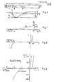
- the structure of the semiconductor diode 1 is shown schematically in FIG.
- the diode 1 like an injection transistor known per se, consists of an npn or a pnp-3 layer structure. with the three adjacent layers 2, 3 and 4.
- the electrodes are 5 and 6 ' denotes and form ohmic contacts.
- the base zone (B), ie the layer 3 is however so short or so thin that its entire area is depleted of free charge carriers even without external voltage being applied. The resulting numerical measure of the thickness d depends on the chosen doping density.
- Equation (1) E is the dielectric constant of the semiconductor used.
- Equation (2) applies to N E »N B » N C.
- the diffusion voltage U D is determined by the thermal voltage U T (U T ⁇ 25 m V at room temperature) and the ratio of emitter to basic doping density N E / N C.
- I S is the saturation current.
- the current I increases as the potential barrier ⁇ R decreases.
- FIG 6 shows the spatial profile of the electrical potential in the diode when the negative voltage is applied.
- Fig. 7 shows the voltage dependence of the potential barriers ⁇ R and ⁇ L.
- U 0, ⁇ R and ⁇ L differ only by the small one, given by Eq. (3) given diffusion voltage U D. With increasing positive voltage, ⁇ R decreases.
- U F the flat ribbon voltage U F , the right potential barrier ⁇ R is completely removed.
- the flat band voltage U F is equal to twice the potential mountain height ⁇ B with thermal equilibrium (see FIG. 4). As the negative voltage increases, ⁇ L becomes smaller and reaches the voltage zero ..
- the ratio of base to subsequentlydotierun g sdich t e N B / N C thus determines the asymmetry of the voltage dependence of ⁇ R and ⁇ L and after the Gln. (4) and (5) also the asymmetry of the current-voltage line.
- Fig. 9 shows current-voltage characteristics for two silicon diodes with different base thickness. The following data were assumed in the calculation:
- FIG. 10 shows another special embodiment of a diode 10 according to the invention, namely one in which the two pn junction areas between the layers 12 and 13 or 13 and 14 have different sizes. These layers 12, 13 and 14 physically correspond to the layers 2 and 3 and 4 already described in detail above.
- the ohmic contacts are denoted by 15 and 16.
- FIG. 10 also shows an example of the use of a diode according to the invention as a photosensitive component, for example as a photovoltaic detector.
- This application is described in accordance with FIG. 10 for the diode 10, but analogously also applies to a diode 1 in accordance with FIG. 1.
- an electromagnetic, in particular light radiation, ultraviolet radiation or also infrared radiation is indicated, which originates, for example, from a light source 22.
- This radiation 21 penetrates through the electrode 15, which is made permeable for this purpose, into the layers 12, 13 and 14 of the diode 10.
- the electrode 15 can also be designed in the form of a ring or a perforation.
- the radiated radiation 21 generates in the diode 10 constructed from the layers 12, 13 and 14 a photovoltaic electrical voltage or a photocurrent which is between the electrical connections 23 and 24 connected to the electrodes 15 and 16 can be removed and can be detected, for example, by the measuring instrument 25.
- a particularly low height of the energy barrier is to be sought, for example for infrared radiation, as can be achieved with the invention in contrast to the prior art.
- layer 12 or layer 2 thin, for example thinner than 1 / um. It is thus achieved that the charge carriers generated in the case of ultraviolet radiation essentially already in the uppermost layer portions of layer 12 can contribute optimally to the photo current or photo voltage generated.
- FIG. 11 shows a basic circuit diagram of such an application with a bipolar transistor 30, between the collector output 31 and base input 32 of which a diode 1 or 10 according to the invention is inserted. With 33 the emitter of the transistor 30 is designated.
- FIG. 12 shows a basic circuit using a diode erfindungsgemäBen 1, 10 as a frequency converting diode, for converting the frequency f 1 of an incoming signal in any frequency f 1 to the harmonic frequency f 2 as the outgoing signal.
- 41 and 42 are Designated resonant circuits in this basic circuit.
- Fig. 13 shows the use of a diode 1, 10 according to the invention in a mixer circuit shown in principle with the input frequencies f 3 and f 4 , from which the output signal of the frequency f 5 is generated.
- tuning circuits are used for tuning.
- a diode With regard to the technological structure of a diode according to the invention, it should also be noted that for the individual layers 2, 3, 4 or 12, 13, 14 of the layer structure, one and the same semiconductor material; E.g .: an elementary semiconductor such as silicon or a compound semiconductor such as gallium arsenide can be used.
- an elementary semiconductor such as silicon
- a compound semiconductor such as gallium arsenide
- advantages can also be achieved if all or even only partially adjacent layers consist of mutually different semiconductor material, e.g. layer 2 or 12 or layer 4 or 14 made of gallium arsenide and the adjacent layer 3 or 13 made of gallium aluminum arsenide.
- a semiconductor material with a direct band transition e.g. Gallium arsenide to be used for one or for all layers 2 to 4 or 12 to 14 of a diode according to the invention.
- a semiconductor-metal composite material such as, for example, aluminum. Silicon material to use.
- a Such composite material is produced, for example, by joint, simultaneous vapor deposition of silicon and aluminum.
Abstract
Halbleiter-Diode (1, 10) mit 3-Schichten-Struktur (2, 34; 12, 13, 14), deren mittlere Schicht (3; 13) so dünn gewählt ist, daß bei der gegebenen Dotierung dieser Schicht der genannte Bereich dieser Schicht schon ohne angelegte Spannung an freien Ladungsträgern verarmt ist. Bevorzugte Verwendung eine solchen Diode als Detektor und als modulierbare Lumineszenzdiode.Semiconductor diode (1, 10) with a 3-layer structure (2, 34; 12, 13, 14), the middle layer (3; 13) of which is selected to be so thin that, given the doping of this layer, said area of this layer Layer is already depleted of free charge carriers without applied voltage. Preferred use of such a diode as a detector and as a modulatable luminescent diode.
Description
Die Erfindung betrifft eine Halbleiter-Diode, wie sie im Oberbegriff des Patentanspruches 1 angegeben ist.The invention relates to a semiconductor diode, as specified in the preamble of
Es ist bekannt, daß sowohl bei pn- als auch bei Schottky-Dioden die Schwellenspannung im wesentlichen durch den Bandabstand des verwendeten Halbleiters bestimmt wird. Für kleine Schwellenspannungen sind i.a. Halbleiter mit geringem Bandabstand erforderlich. Die Herstellung schmalbandiger Halbleiter-Dioden ist zur Zeit allerdings noch sehr schwierig und aufwendig.It is known that in both pn and Schottky diodes the threshold voltage is essentially determined by the bandgap of the semiconductor used. For small threshold voltages, i.a. Semiconductors with a small bandgap are required. However, the manufacture of narrowband semiconductor diodes is currently still very difficult and expensive.
Ferner ist bekannt, daß bei pn-Dioden Minoritätsträger-und bei Schottky-Dioden Majoritätsträgereffekte dominieren. Dementsprechend haben Schottky-Dioden wesentlich höhere Grenzfrequenzen als pn-Dioden.It is also known that minority carrier effects dominate in pn diodes and majority carrier effects dominate in Schottky diodes. Accordingly, Schottky diodes have significantly higher cutoff frequencies than pn diodes.
Aus "Solid State Electronics" (1976) Bd.19, Seiten 625-631 ist eine sogenannte Baritt-pn-Diode bekannt, die als Generator zur Erzeugung sehr hoher Frequenzen, z.B. 10 GHz, verwendet wird. In dieser Diode werden Laufzeiteffekte ausgenutzt,-die im wesentlichen in der mittleren Zwischenschicht der Diode auftreten. Diese Zwischenschicht weist,wie die Fig.1 dieser Druckschrift zeigt, einen Aufbau und eine Dotierung auf, bei der ohne angelegte äußere Spannung, abgesehen von den äußersten Randbereichen, praktisch keine Verarmung an freien Ladungsträgern vorliegt. Die zur Ausnutzung der Laufzeiteffekte erforderlichen hohen Feldstärken in dieser Zwischenschicht bedingen, daß diese Zwischenschicht eine erhebliche Mindestdotierung aufweist. Die wiederum durch die vorgegebene zu erzeugende Frequenz bedingte Dicke dieser Zwischenschicht führt dazu, daß nur die bereits erwähnten Randbereiche an freien Ladungsträgern verarmt sind.A so-called Baritt-pn diode is known from "Solid State Electronics" (1976) Vol. 19, pages 625-631, which is used as a generator for generating very high frequencies, for example 10 GHz. In this diode run time effects are used, which essentially occur in the middle intermediate layer of the diode. As shown in FIG. 1 of this document, this intermediate layer has a structure and a doping in which, without the application of external voltage, apart from the outermost edge regions, there is practically no depletion of free charge carriers. The high field strengths required in this intermediate layer to utilize the runtime effects mean that this intermediate layer has a considerable minimum doping. The thickness of this intermediate layer, which is in turn caused by the predetermined frequency to be generated, means that only the edge regions already mentioned are depleted of free charge carriers.
Ebenfalls zur Erzeugung von Hochfrequenz dient eine aus der DE-OS 22 24 159 bekannte Lawinenlaufzeit-Diode, die aus zwei auf einer Metallelektrode übereinanderliegenden p- und n-Halbleiterschichten aufgebaut ist. Die bei diesem Heteroaufbau mittlere Schicht soll eine vergleichsweise zur darüberliegenden Halbleiterschihht eine um ca. zwei Größenordnungen höhere Dotierung aufweisen, so daß bei fehlender Betriebsspannung auch bei einer solchen Diode praktisch nur Randbereiche dieser mittleren Schicht eine Verarmung an freien Ladungsträgern aufweisen, wie dies im übrigen von jeglichem pn-Übergang bekannt ist.An avalanche delay diode known from DE-OS 22 24 159 is also used to generate high frequency and is constructed from two p- and n-semiconductor layers one on top of the other on a metal electrode. The middle layer in this heterogeneous structure should have a doping that is about two orders of magnitude higher than that of the semiconductor layer above it, so that when there is no operating voltage, even with such a diode practically only peripheral areas of this middle layer are depleted of free charge carriers, as is the case in the rest of any pn transition is known.
Es ist eine Aufgabe der vorliegenden Erfindung, eine solche Halbleiter-Diode zu schaffen, die eine jeweils (technologisch) fest vorgebbare höhe ihrer Energiebarriere hat, die unterhalb des durch den üblichen pn-Ubergang vorgegebenen Wert liegt. Insbesondere ist es eine Aufgabe der vorliegenden Erfindung, ein - nämlich aufgrund der verringerten Höhe der Energiebarriere - in seiner Empfindlichkeit verbessertes Fotoelement zu schaffen.It is an object of the present invention to provide such a semiconductor diode which has a (technologically) predeterminable height of its energy barrier which is below the value given by the usual pn transition. In particular, it is an object of the present invention to provide a photo element which is improved in sensitivity, namely because of the reduced height of the energy barrier.
Diese Aufgabe wird mit einer Halbleiter-Diode nach dem Oberbegriff des Patentanspruches 1 erfindungsgemäß gelöst, wie dies im Kennzeichen des Patentanspruches 1 angegeben ist. Weitere Ausgestaltungen und auf der Erfindung beruhende weitere vorteilhafte Anwendungen der Erfindung gehen aus den Unteransprüchen hervor.This object is achieved according to the invention with a semiconductor diode according to the preamble of
Der.Erfindung liegt der Gedanke zugrunde, eine 3-Schichtstruktur aufzubauen, die entweder aus einer npn-Schicht-oder einer pnp-Schichtfolge besteht, bei der jedoch im Gegensatz zum Injektionstransistor die mittlere Schicht so dünn ist, daß bei wahlweise vorgegebener Dotierungshöhe dieser mittleren Schicht der gesamte Bereich dieser mittleren Schicht bereits ohne äußere angelegte elektrische Spannung von freien Ladungsträgern verarmt ist.The invention is based on the idea of building up a 3-layer structure which consists of either an npn-layer or a pnp-layer sequence, but in which, in contrast to the injection transistor, the middle layer is so thin that the middle layer is optionally given a doping level Layer the entire area of this middle layer is already depleted of free charge carriers without external electrical voltage.
Für die Herstellung solcher Dioden eignen sich folgende an sich bekannte Verfahren:
- a) Ionenimplantation,
- b) Molekularstrahlepitaxie.
- a) ion implantation,
- b) Molecular beam epitaxy.
Die mit der Erfindung erzielten Vorteile bestehen insbesondere darin, daß die Schwellenspannung der Diode über technologische Parameter wie Dotierungsdichte oder Schichtdicke kontinuierlich im Bereich zwischen der thermischen Spannung UT und der Diffusionsspannung UD eingestellt werden kann. Bei Zimmertemperatur betragen UT ≃ 25 mV und UD ≃ 1 Y. Es ist daher z.B. möglich, Silizium-Dioden mit sehr kleinen Schwellenspannungen zu realisieren.The advantages achieved with the invention consist particularly in the fact that the threshold voltage of the diode can be adjusted continuously in the region between the thermal voltage U T U D and the diffusion voltage of technological parameters such as doping density or layer thickness. At room temperature, U T ≃ 25 mV and U D ≃ 1 Y. It is therefore possible, for example, to implement silicon diodes with very low threshold voltages.
Ein weiterer Vorteil besteht darin, daß wegen des dominierenden Majoritätsträgerstromes die Diode bis zu sehr hohen Frequenzen eingesetzt werden kann.Another advantage is that because of the dominant majority carrier current, the diode can be used up to very high frequencies.
Die Erfindung wird nun anhand der in der Zeichnung dargestellten Figuren näher erläutert und beschrieben. Es zeigen
- Fig.1 schematisch den Aufbau der Halbleiter-Diode nach der Erfindung,
- Fig.2 den Verlauf der Raumladungsdichte in der Diode bei thermischem Gleichgewicht,
- Fig.3 den Verlauf der elektrischen Feldstärke bei thermischem Gleichgewicht,
- Fig.4 den Verlauf des elektrischen Potentials bei ther- : mischem Gleichgewicht,
- Fig.5 den Verlauf des elektrischen Potentials bei angelegter positiver Spannung,
- Fig.6 den Verlauf des elektrischen Potentials bei angelegter negativer Spannung,
- Fig.7 die Potentialbarriere φR und φL in Abhängigkeit der angelegten Spannung,
- Fig.8 den prinzipiellen Verlauf der Strom-Spannungskennlinie,
- Fig.9 Strom-Spannungskennlinien für zwei Dioden mit unterschiedlicher Basisdicke, .
- Fig.10 eine andere Ausführungsform einer erfindungsgemäBen Diode mit einem Aufbau nach Art einer Mesa-Struktur, wobei diese Diode auch in ihrer Verwendung als foto-voltaischer Detektor gezeigt ist,
- Fig.11 Prinzipschaltbilder zu Verwendungen einer erfinbis 13 dugsgemäßen Diode als Klammer-Diode (Fig.11), als Frequenzwandler (Fig.12) und als Mischer (Fig.13).
- 1 schematically shows the structure of the semiconductor diode according to the invention,
- 2 shows the course of the space charge density in the diode with thermal equilibrium,
- 3 shows the course of the electric field strength with thermal equilibrium,
- 4 shows the course of the electrical potential with thermal equilibrium,
- 5 shows the course of the electrical potential when positive voltage is applied,
- 6 shows the course of the electrical potential when a negative voltage is applied,
- 7 shows the potential barrier φ R and φ L as a function of the applied voltage,
- 8 shows the basic course of the current-voltage characteristic,
- 9 shows current-voltage characteristics of two diodes with different base icke d.
- 10 shows another embodiment of a erfindungsgemäBen diode with a structure in the manner of a mesa structure, this diode is also shown in their use as photo-volta i shear detector,
- Fig. 11 Basic circuit diagrams for the use of a diode according to the invention in accordance with the invention as a clamp diode (Fig. 11), as a frequency converter (Fig. 12) and as a mixer (Fig. 13).
In Fig.1 ist der Aufbau der Halbleiter-Diode 1 schematisch dargestellt. Die Diode 1 besteht wie ein an sich bekannter Injektionstransistor aus einer npn- oder einer pnp-3-Schichtstruktur. mit den drei aneinandergrenzenden Schichten 2,3 und 4. Die Elektroden sind mit 5 und 6' bezeichnet und bilden ohmsche Kontakte. Im Gegensatz zum bekannten Injektionstransistor ist bei der Erfindung die Basiszone (B), d.h. die Schicht 3, jedoch so kurz bzw. so dünn, daß bereits ohne äußere angelegte Spannung ihr gesamter Bereich von freien Ladungsträgern verarmt ist. Das sich dabei ergebende zahlenmäßige Maß der Dicke d ist abhängig von der gewählten Dotierungsdichte.The structure of the
Fig.2 zeigt den örtlichen Verlauf der Raumladungsdichte in der Diode 1 bei thermischem Gleichgewicht, d.h. ohne äußere angelegte Spannung. Die Basis (B) bzw. Schicht 3 enthält im Gegensatz zum bekannten injektionstransistor bei der Erfindung keinen neutralen Bereich. Die Raumladungsdichten in den einzelnen Zonen werden durch die entsprechenden Dotierungsdichten bestimmt. In Fig.2 sind NE, NB und Ne die Dotierungsdichten in Emitter (E), Basis (B) und Kollektor (C) und e = 1,6.10-19 As die Elementarladung.2 shows the local course of the space charge density in the
In Fig.3 ist der örtliche Verlauf der elektrischen Feldstärke EX in der Diode wiederum für thermisches Gleichgewicht dargestellt, der aus der Raumladungsdichte eN(x) durch folgende Integration hervorgeht:
in Gleichung (1) ist E die Dielektrizitäzskonstante des verwendeten Halbleiters.in equation (1) E is the dielectric constant of the semiconductor used.
Fig.4 stellt den räumlichen Verlauf des elektrischen Potentials V(x) in der Diode 1 bei thermischem Gleichgewicht dar. Die Höhe des Potentialberges φB hängt von der Dicke d und der Dotierungsdichte NB der Basis wie folgt ab:
Aus Gleichung (2) geht hervor, daß die Potentialberghöhe φB durch d und NB technologisch eingestellt werden kann.From equation (2) it follows that the potential mountain height φ B can be set technologically by d and N B.
Für die Diffusionsspannung UD gilt:
Die Diffusionsspannung UD wird durch die thermische Spannung UT (UT ≃ 25 mV bei Zimmertemperatur) und das Verhältnis von Emitter- zu Basisdotierungsdichte NE/NC bestimmt.The diffusion voltage U D is determined by the thermal voltage U T (U T ≃ 25 m V at room temperature) and the ratio of emitter to basic doping density N E / N C.
Fig. 5 zeigt den räumlichen Verlauf des elektrischen Potentials in der Diode bei angelegter positiver Spannung. Die Raumladungszonen werden dabei so verschoben, daß die rechte Potentialbarriere ;R kleiner wird als die linke, φL. Es gelangen somit mehr Majoritätsträger vom Kollektor (C) zum Emitter (E) als umgekehrt. Der resultierende elektrische Strom I läßt sich berechnen aus:
In Gl. (4) ist IS der Sättigungsstrom. Der Strom I steigt mit kleiner werdender Potentialbarriere φR.In Eq. (4) I S is the saturation current. The current I increases as the potential barrier φ R decreases.
In Fig. 6 ist der räumliche Verlauf des elektrischen Potentials in der Diode bei angelegter negativer Spannung dargestellt.6 shows the spatial profile of the electrical potential in the diode when the negative voltage is applied.
In diesem Fall ergibt die Verschiebung der Raumladungszonen eine kleinere linke Potentialbarriere φL. Für den elektrischen Strom I erhält man entsprechend:
Fig. 7 zeigt die Spannungsabhängigkeit der Potentialbarrieren φR und φL. Bei U = 0 unterscheiden sich φR und φL lediglich um die kleine, durch Gl. (3) gegebene Diffusionsspannung UD. Mit steigender positiver Spannung sinkt φR. Bei der Flachbandspannung UF ist die rechte Potentialbarriere φR ganz abgebaut. Für NE» NB » NC gilt: .
Die Flachbandspannung UF ist gleich der doppelten Potentialberghöhe φB bei thermischem Gleichgewicht ( siehe Fig. 4). Mit wachsender negativer Spannung wird φL kleiner und erreicht bei der Spannung ![]()
![]()
In Fig. 8 ist der prinzipielle Verlauf der Strom-Spannungskennlinie dargestellt. Während bei positiven Spannungen der Strom I in der Nähe der Flachbandspannung UF stark ansteigt, geschieht dies im Sperrbereich der Diode erst bei Spannungen in der Gegend von ![]()

- Is Sättigungsstrom
- UF Flachbandspannung, nach Gl. (6) mit NB und d technologisch einstellbar
- UT ' Thermische Spannung (UT ≃ 25 mV bei Zimmertemperatur
- NB,C Dotierungsdichten von Basis bzw. Kollektor
- I s saturation current
- U F ribbon tension, according to Eq. (6) Technologically adjustable with N B and d
- U T ' thermal voltage (U T ≃ 25 mV at room temperature
- N B, C doping densities of base or collector
Fig. 9 zeigt Strom-Spannungskennlinien für zwei Silizium-Dioden mit unterschiedlicher Basisdicke. Es wurden bei der Berechnung folgende Daten angenommen:


Aus Fig.9 geht hervor, daß bei beiden Dioden die Schwellenspannung kleiner als 0,5 V ist. Das Sperrverhalten richtet sich nach dem Verhältnis von NB/NC (siehe Fig.8). Bei größerem Unterschied der Dotierungsdichten NB und NC wird das Sperrverhalten der Dioden ausgeprägter.9 shows that the threshold voltage for both diodes is less than 0.5 V. The locking behavior depends on the ratio of N B / N C (see Fig. 8). If the doping densities N B and N C differ, the blocking behavior of the diodes becomes more pronounced.
Fig.10 zeigt eine andere spezielle Ausführungsform einer erfindungsgemäßen Diode 10, nämlich einer solchen, bei der die beiden pn-Ubergangsflächen zwischen den Schichten 12 und 13 bzw. 13 und 14 verschiedene Größe haben. Diese Schichten 12, 13 und 14 entsprechen physikalisch den bereits oben ausführlich beschriebenen Schichten 2 und 3 und 4. Die ohmschen Kontakte sind mit 15 und 16 bezeichnet.10 shows another special embodiment of a diode 10 according to the invention, namely one in which the two pn junction areas between the
Aus der Fig.10 geht des weiteren ein Beispiel für die Anwendung einer erfndungsgemätßen Diode als fotoempfindliches Bauelement, z.B. als foto-voltaischer Detektor, hervor. Diese Anwendung ist der Fig.10 entsprechend für die Diode 10 beschrieben, gilt aber sinngemäß auch für eine Diode 1 nach der Fig.1. Mit 21 ist eine elektromagnetische, insbesondere Lichtstrahlung, Ultraviolettstrahlung oder auch Infrarotstrahlung angedeutet, die z.B. von einer Lichtquelle 22 herrührt. Diese Strahlung 21 dringt durch die zu diesem Zweck durchlässig ausgeführte Elektrode 15 hindurch in die Schichten 12, 13 und 14 der Diode 10 ein. Statt einer Durchlässigkeit der Diode 15 kann die Elektrode 15 auch ringförmig oder perforiert ausgebildet sein. Die eingestrahlte Strahlung 21 erzeugt in der aus den Schichten 12, 13 und 14 aufgebaute Diode 10 eine foto-volta'sche elektrische Spannung bzw. einen Fotostrom, der zwischen den mit den Elektroden 15 bzw. 16 verbundenen elektrischen Anschlüssen 23 und 24 abgenommen werden kann und z.B. durch das Meßinstrument 25 nachzuweisen ist.FIG. 10 also shows an example of the use of a diode according to the invention as a photosensitive component, for example as a photovoltaic detector. This application is described in accordance with FIG. 10 for the diode 10, but analogously also applies to a
Entsprechend der Quantenenergie der jeweils beispielsweise nachzuweisenden Strahlung 21 ist z.B. für Infrarotstrahlung eine besonders niedrige Höhe der Energiebarriere anzustreben, wie dies mit der Erfindung im Gegensatz zum Stand der Technik realisierbar ist. Speziell für ultraviolette Strahlung 21 empfiehlt es sich, die Schicht 12, bzw. die Schicht 2, dünn - z.B. dünner als 1/um - auszubilden. Damit ist erreicht, daß die bei ultraviolettstrahlung im wesentlichen bereits in den obersten Schichtanteilen der Schicht 12 erzeugten Ladungsträger optimal zum erzeugten Fotostrom bzw. zur erzeugten Fotospannung beitragen können.In accordance with the quantum energy of the
Andere Anwendungen der Erfindung unter Ausnutzuag der erfindungsgemäß herabsetzbaren Energiebarriere sind die Verwendung einer erfindungsgemäßen Diode als Klammer-diode (clamping Diode) in Verbindung mit Bipolartransistoren, nämlich zur Erhöhung deren Schaltgeschwindigkeit.Other applications of the invention using the energy barrier that can be reduced according to the invention are the use of a diode according to the invention as a clamping diode in connection with bipolar transistors, namely to increase their switching speed.
Fig.11 zeigt ein Prinzipschaltbild einer solchen Anwendung mit einem Bipolartransistor 30, zwischen dessen Kollektorausgang 31 und Basiseingang 32 eine wie erfindvngsgemäße Diode 1 bzw. 10 eingefügt ist. Mit 33 ist der Emitter des Transistors 30 bezeichnet.11 shows a basic circuit diagram of such an application with a
Fig.12 zeigt eine Prinzipschaltung der Verwendung einer erfindungsgemäBen Diode 1, 10 als Frequenzwandler-Diode, zur Umwandlung der Frequenz f1 eines eingehenden Signals in irgendeine zur Frequenz f1 harmonische Frequenz f2 als ausgehendes Signal. Mit 41 und 42 sind Schwingkreise in dieser Prinzipschaltung bezeichnet.12 shows a basic circuit using a
Fig.13 zeigt die Anwendung einer erfindungsgemäßen Diode 1, 10 in einer dem Prinzip nach dargestellten Mischerschaltung mit den Eingangsfrequenzen f3 und f4, aus denen das Ausgangssignal der Frequenz f5 erzeugt wird. Mit 51, 52, 53 sind der Abstimmung dienende Schwingkreise bezeichnet.Fig. 13 shows the use of a
Zum technologischen Aufbau einer erfindungsgemäßen Diode ist noch anzumerken, daß für die einzelnen Schichten 2, 3, 4 bzw. 12, 13, 14 der Schichtstruktur ein und dasselbe Halbleitermaterial; z.B: ein Elementhalbleiter wie Silizium oder auch ein Verbindungshalbleiter wie Galliumarsenid, verwendet werden kann. Vorteile können aber auch erreicht werden, wenn alle oder auch nur teilweise jeweils benachbarte Schichten aus zueinander jeweils verschiedenem Halbleitermaterial bestehen, wie z.B. die Schicht 2 oder 12 bzw. die Schicht 4 oder 14 aus Galliumarsenid und die benachbarte Schicht 3 oder 13 aus Gallium-Aluminiumarsenid.With regard to the technological structure of a diode according to the invention, it should also be noted that for the
Insbesondere im Zusammenhang mit Lumineszenz ist es vorteilhaft, ein Halbleitermaterial mit direktem Bandübergang, z.B. Galliumarsenid, für jeweils eine oder auch für alle Schichten 2 bis 4 bzw. 12 bis 14 einer erfindungsgemäßen Diode zu verwenden.In particular in connection with luminescence, it is advantageous to use a semiconductor material with a direct band transition, e.g. Gallium arsenide to be used for one or for all
Für jeweils eine oder beide Elektroden einer erfindungsgemäßen Diode ist es für das Erreichen besserer ohmscher Kontakte und/oder zur Vermeidung eines Durchlegierens des Materials des Kontaktes bei den bei der Erfindung insbesondere dünnen Halbleiterschichten von Vorteil, ein Halbleiter-Metall-Verbundmaterial, wie z.B. Aluminium-Silizium-Material, zu verwenden. Ein solches Verbundmaterial wird z.B. durch gemeinsames, gleichzeitiges Aufdampfen von Silizium und Aluminium hergestellt.For one or both electrodes of a diode according to the invention, it is advantageous to achieve better ohmic contacts and / or to avoid alloying of the material of the contact in the semiconductor layers, which are particularly thin in accordance with the invention, a semiconductor-metal composite material such as, for example, aluminum. Silicon material to use. A Such composite material is produced, for example, by joint, simultaneous vapor deposition of silicon and aluminum.
- d Dicke der Basiszoned Base zone thickness
- e Elementarladunge Elementary charge
- ε Dielektrizitätskonstente des verwendeten Halbleitersε dielectric constant of the semiconductor used
- Ex elektrische FeldstärkeE x electric field strength
- I elektrischer StromI electric current
- Is SättigungsstromI s saturation current
- NE Dotierungsdichte des EmittersN E doping density of the emitter
- NB Dotierungsdichte der BasisN B doping density of the base
- NC Dotierungsdichte des KollektorsN C doping density of the collector
- U angelegte SpannungU applied voltage
- UD DiffusionsspannungU D diffusion voltage
- UF FlachbandspannungU F ribbon tension
- V elektrisches PotentialV electrical potential
- PotentialbarrierePotential barrier
- φB Potentialbarriere bei thermiechem Geichgewichtφ B potential barrier with thermal balance
- φL,B Poteatialbarrieren bei angelegter Spannungφ L, B Potential barriers with voltage applied
- σ Raumladtzagadichteσ Raumladtzagadichte
Claims (15)
Applications Claiming Priority (2)
| Application Number | Priority Date | Filing Date | Title |
|---|---|---|---|
| DE2800820 | 1978-01-10 | ||
| DE19782800820 DE2800820A1 (en) | 1978-01-10 | 1978-01-10 | SEMICONDUCTOR DIODE |
Publications (3)
| Publication Number | Publication Date |
|---|---|
| EP0003130A2 true EP0003130A2 (en) | 1979-07-25 |
| EP0003130A3 EP0003130A3 (en) | 1979-08-22 |
| EP0003130B1 EP0003130B1 (en) | 1981-02-11 |
Family
ID=6029211
Family Applications (1)
| Application Number | Title | Priority Date | Filing Date |
|---|---|---|---|
| EP79100063A Expired EP0003130B1 (en) | 1978-01-10 | 1979-01-10 | Three-layer semiconductor diode and its application |
Country Status (6)
| Country | Link |
|---|---|
| US (1) | US4278986A (en) |
| EP (1) | EP0003130B1 (en) |
| JP (1) | JPS54133085A (en) |
| DE (2) | DE2800820A1 (en) |
| ES (1) | ES476675A1 (en) |
| GR (1) | GR75591B (en) |
Cited By (5)
| Publication number | Priority date | Publication date | Assignee | Title |
|---|---|---|---|---|
| EP0028022A2 (en) * | 1979-10-25 | 1981-05-06 | Siemens Aktiengesellschaft | Infra-red sensitive x-y-CCD sensor and method of manufacturing it |
| GB2116774A (en) * | 1982-03-09 | 1983-09-28 | Semitron Cricklade Ltd | Transient absorption semiconductor device for voltage surge protection |
| DE3237379A1 (en) * | 1982-10-08 | 1984-04-12 | Siemens AG, 1000 Berlin und 8000 München | TRANSISTOR WITH ADJUSTABLE ENERGY BARRIER AND ITS USE |
| DE3240180A1 (en) * | 1982-10-29 | 1984-05-03 | Siemens AG, 1000 Berlin und 8000 München | Semiconductor radiation detector, in particular for infrared radiation |
| US5047355A (en) * | 1983-09-21 | 1991-09-10 | Siemens Aktiengesellschaft | Semiconductor diode and method for making it |
Families Citing this family (13)
| Publication number | Priority date | Publication date | Assignee | Title |
|---|---|---|---|---|
| US5053845A (en) * | 1980-05-23 | 1991-10-01 | Ricoh Company, Ltd. | Thin-film device |
| US4410902A (en) * | 1981-03-23 | 1983-10-18 | The United States Of America As Represented By The Secretary Of The Army | Planar doped barrier semiconductor device |
| DE3210086A1 (en) * | 1982-03-19 | 1983-09-22 | Siemens AG, 1000 Berlin und 8000 München | LUMINESCENCE DIODE, SUITABLE AS PRESSURE SENSOR |
| GB2121600A (en) * | 1982-05-10 | 1983-12-21 | Philips Electronic Associated | Gate controlled unipolar hot-carrier transistors |
| US4596069A (en) * | 1984-07-13 | 1986-06-24 | Texas Instruments Incorporated | Three dimensional processing for monolithic IMPATTs |
| US4596070A (en) * | 1984-07-13 | 1986-06-24 | Texas Instruments Incorporated | Interdigitated IMPATT devices |
| DE3708474A1 (en) * | 1987-03-16 | 1988-09-29 | Licentia Gmbh | Majority-carrier semiconductor component and method of fabricating it |
| DE3876869D1 (en) * | 1987-06-22 | 1993-02-04 | Landis & Gyr Betriebs Ag | ULTRAVIOLET PHOTODETECTOR AND METHOD FOR PRODUCING THE SAME. |
| US5113076A (en) * | 1989-12-19 | 1992-05-12 | Santa Barbara Research Center | Two terminal multi-band infrared radiation detector |
| US7649496B1 (en) | 2004-10-12 | 2010-01-19 | Guy Silver | EM rectifying antenna suitable for use in conjunction with a natural breakdown device |
| US8987858B2 (en) * | 2013-03-18 | 2015-03-24 | General Electric Company | Method and system for transient voltage suppression |
| US11264373B2 (en) | 2019-12-21 | 2022-03-01 | Intel Corporation | Die backend diodes for electrostatic discharge (ESD) protection |
| US11424239B2 (en) * | 2019-12-21 | 2022-08-23 | Intel Corporation | Diodes for package substrate electrostatic discharge (ESD) protection |
Citations (2)
| Publication number | Priority date | Publication date | Assignee | Title |
|---|---|---|---|---|
| FR2284987A1 (en) * | 1974-09-10 | 1976-04-09 | Thomson Csf | PARTICULAR SEMI-CONDUCTIVE STRUCTURE OF THERMOIONIC INJECTION DIODE WITH LOW NOISE |
| FR2288398A1 (en) * | 1974-10-19 | 1976-05-14 | Sony Corp | SEMICONDUCTOR PHOTOELECTRIC DEVICE |
Family Cites Families (2)
| Publication number | Priority date | Publication date | Assignee | Title |
|---|---|---|---|---|
| GB1573309A (en) * | 1976-03-24 | 1980-08-20 | Mullard Ltd | Semiconductor devices and their manufacture |
| US4167748A (en) * | 1978-07-03 | 1979-09-11 | Bell Telephone Laboratories, Incorporated | High voltage monolithic transistor circuit |
-
1978
- 1978-01-10 DE DE19782800820 patent/DE2800820A1/en not_active Withdrawn
-
1979
- 1979-01-02 US US06/000,103 patent/US4278986A/en not_active Expired - Lifetime
- 1979-01-09 GR GR58052A patent/GR75591B/el unknown
- 1979-01-09 ES ES476675A patent/ES476675A1/en not_active Expired
- 1979-01-10 JP JP212279A patent/JPS54133085A/en active Pending
- 1979-01-10 DE DE7979100063T patent/DE2960132D1/en not_active Expired
- 1979-01-10 EP EP79100063A patent/EP0003130B1/en not_active Expired
Patent Citations (2)
| Publication number | Priority date | Publication date | Assignee | Title |
|---|---|---|---|---|
| FR2284987A1 (en) * | 1974-09-10 | 1976-04-09 | Thomson Csf | PARTICULAR SEMI-CONDUCTIVE STRUCTURE OF THERMOIONIC INJECTION DIODE WITH LOW NOISE |
| FR2288398A1 (en) * | 1974-10-19 | 1976-05-14 | Sony Corp | SEMICONDUCTOR PHOTOELECTRIC DEVICE |
Cited By (8)
| Publication number | Priority date | Publication date | Assignee | Title |
|---|---|---|---|---|
| EP0028022A2 (en) * | 1979-10-25 | 1981-05-06 | Siemens Aktiengesellschaft | Infra-red sensitive x-y-CCD sensor and method of manufacturing it |
| EP0028022A3 (en) * | 1979-10-25 | 1984-06-06 | Siemens Aktiengesellschaft | Infra-red sensitive x-y-ccd sensor and method of manufacturing it |
| GB2116774A (en) * | 1982-03-09 | 1983-09-28 | Semitron Cricklade Ltd | Transient absorption semiconductor device for voltage surge protection |
| DE3237379A1 (en) * | 1982-10-08 | 1984-04-12 | Siemens AG, 1000 Berlin und 8000 München | TRANSISTOR WITH ADJUSTABLE ENERGY BARRIER AND ITS USE |
| EP0106254A2 (en) * | 1982-10-08 | 1984-04-25 | Siemens Aktiengesellschaft | Transistor with an adjustable energy barrier, and its application |
| EP0106254A3 (en) * | 1982-10-08 | 1986-12-10 | Siemens Aktiengesellschaft | Transistor with an adjustable energy barrier, and its application |
| DE3240180A1 (en) * | 1982-10-29 | 1984-05-03 | Siemens AG, 1000 Berlin und 8000 München | Semiconductor radiation detector, in particular for infrared radiation |
| US5047355A (en) * | 1983-09-21 | 1991-09-10 | Siemens Aktiengesellschaft | Semiconductor diode and method for making it |
Also Published As
| Publication number | Publication date |
|---|---|
| DE2960132D1 (en) | 1981-03-26 |
| ES476675A1 (en) | 1979-11-01 |
| US4278986A (en) | 1981-07-14 |
| DE2800820A1 (en) | 1979-09-27 |
| JPS54133085A (en) | 1979-10-16 |
| EP0003130B1 (en) | 1981-02-11 |
| GR75591B (en) | 1984-08-01 |
| EP0003130A3 (en) | 1979-08-22 |
Similar Documents
| Publication | Publication Date | Title |
|---|---|---|
| EP0003130B1 (en) | Three-layer semiconductor diode and its application | |
| DE2546232C2 (en) | Semiconductor photocell | |
| DE3011484C2 (en) | Optically controllable semiconductor device | |
| DE891580C (en) | Photoelectric semiconductor devices | |
| DE2412699C2 (en) | Charge coupled semiconductor device | |
| DE2439875C2 (en) | Semiconductor component with negative resistance characteristics | |
| DE3136528A1 (en) | SEMICONDUCTOR AVALANCHE PHOTODETECTOR | |
| DE1264513B (en) | Voltage-free differential amplifier circuit | |
| DE3135462A1 (en) | MONOLITHIC INPUT STAGE OF AN OPTICAL RECEIVER | |
| DE1811492A1 (en) | Field effect transistor | |
| DE3215083A1 (en) | MAJORITY CARGO PHOTODETECTOR | |
| DE19753673A1 (en) | Schottky diode with substrate having two layers of different impurity concentration | |
| DE3526826A1 (en) | STATIC INDUCTION TRANSISTOR AND SAME INTEGRATED CIRCUIT | |
| DE2740203A1 (en) | CARGO TRANSFER ARRANGEMENT | |
| DE2311646A1 (en) | ELECTROLUMINESCENT SEMI-CONDUCTOR ARRANGEMENT | |
| DE2634304C2 (en) | Injection logic semiconductor integrated device comprising two vertical transistors | |
| DE2848925A1 (en) | AVALANCHE PHOTODIODE WITH HETEROUEBERGANG | |
| DE3149101A1 (en) | "SCHOTTKY TRANSITION FIELD EFFECT TRANSISTOR" | |
| DE3241176A1 (en) | METHOD FOR ACHIEVING A STOSSIONIZATION COEFFICIENT RELATIONSHIP BY CONNECTING VARIOUS SEMICONDUCTORS | |
| DE1639177C3 (en) | Monolithically integrated rectifier circuit | |
| EP0103084B1 (en) | Method of making a planar avalanche photodiode having a longwave sensitivity limit above 1.3 um | |
| DE3512385A1 (en) | AVALANCHE PHOTODETECTOR | |
| DE1639259C3 (en) | Switchable semiconductor component and circuit arrangement for its bistable operation | |
| DE2518529C2 (en) | Circuit arrangement for amplifying | |
| DE2112001A1 (en) | Electronic solid body device to utilize the difference in effective mass |
Legal Events
| Date | Code | Title | Description |
|---|---|---|---|
| PUAI | Public reference made under article 153(3) epc to a published international application that has entered the european phase |
Free format text: ORIGINAL CODE: 0009012 |
|
| PUAL | Search report despatched |
Free format text: ORIGINAL CODE: 0009013 |
|
| AK | Designated contracting states |
Designated state(s): BE CH DE FR GB IT NL SE |
|
| AK | Designated contracting states |
Designated state(s): BE CH DE FR GB IT NL SE |
|
| 17P | Request for examination filed | ||
| ITF | It: translation for a ep patent filed |
Owner name: STUDIO JAUMANN |
|
| GRAA | (expected) grant |
Free format text: ORIGINAL CODE: 0009210 |
|
| AK | Designated contracting states |
Designated state(s): BE CH DE FR GB IT NL SE |
|
| REF | Corresponds to: |
Ref document number: 2960132 Country of ref document: DE Date of ref document: 19810326 |
|
| PGFP | Annual fee paid to national office [announced via postgrant information from national office to epo] |
Ref country code: FR Payment date: 19821230 Year of fee payment: 5 |
|
| PGFP | Annual fee paid to national office [announced via postgrant information from national office to epo] |
Ref country code: SE Payment date: 19821231 Year of fee payment: 5 |
|
| PGFP | Annual fee paid to national office [announced via postgrant information from national office to epo] |
Ref country code: NL Payment date: 19830131 Year of fee payment: 5 |
|
| PGFP | Annual fee paid to national office [announced via postgrant information from national office to epo] |
Ref country code: DE Payment date: 19830323 Year of fee payment: 5 |
|
| PGFP | Annual fee paid to national office [announced via postgrant information from national office to epo] |
Ref country code: CH Payment date: 19830331 Year of fee payment: 5 Ref country code: BE Payment date: 19830331 Year of fee payment: 5 |
|
| PG25 | Lapsed in a contracting state [announced via postgrant information from national office to epo] |
Ref country code: SE Effective date: 19840111 |
|
| PG25 | Lapsed in a contracting state [announced via postgrant information from national office to epo] |
Ref country code: CH Effective date: 19840131 Ref country code: BE Effective date: 19840131 |
|
| BERE | Be: lapsed |
Owner name: MADER HERMANN Effective date: 19840110 |
|
| PG25 | Lapsed in a contracting state [announced via postgrant information from national office to epo] |
Ref country code: NL Effective date: 19840801 |
|
| NLV4 | Nl: lapsed or anulled due to non-payment of the annual fee | ||
| PG25 | Lapsed in a contracting state [announced via postgrant information from national office to epo] |
Ref country code: FR Free format text: LAPSE BECAUSE OF NON-PAYMENT OF DUE FEES Effective date: 19840928 |
|
| REG | Reference to a national code |
Ref country code: CH Ref legal event code: PL |
|
| PG25 | Lapsed in a contracting state [announced via postgrant information from national office to epo] |
Ref country code: DE Effective date: 19841002 |
|
| GBPC | Gb: european patent ceased through non-payment of renewal fee | ||
| REG | Reference to a national code |
Ref country code: FR Ref legal event code: ST |
|
| PG25 | Lapsed in a contracting state [announced via postgrant information from national office to epo] |
Ref country code: GB Effective date: 19881117 |
|
| EUG | Se: european patent has lapsed |
Ref document number: 79100063.1 Effective date: 19850605 |
|
| PLBE | No opposition filed within time limit |
Free format text: ORIGINAL CODE: 0009261 |
|
| STAA | Information on the status of an ep patent application or granted ep patent |
Free format text: STATUS: NO OPPOSITION FILED WITHIN TIME LIMIT |