DE19933552B4 - Method for producing an optoelectronic semiconductor device with a ZnO buffer layer - Google Patents
Method for producing an optoelectronic semiconductor device with a ZnO buffer layer Download PDFInfo
- Publication number
- DE19933552B4 DE19933552B4 DE19933552A DE19933552A DE19933552B4 DE 19933552 B4 DE19933552 B4 DE 19933552B4 DE 19933552 A DE19933552 A DE 19933552A DE 19933552 A DE19933552 A DE 19933552A DE 19933552 B4 DE19933552 B4 DE 19933552B4
- Authority
- DE
- Germany
- Prior art keywords
- zno
- buffer layer
- lattice constant
- constant
- axis
- Prior art date
- Legal status (The legal status is an assumption and is not a legal conclusion. Google has not performed a legal analysis and makes no representation as to the accuracy of the status listed.)
- Expired - Fee Related
Links
Classifications
-
- H—ELECTRICITY
- H01—ELECTRIC ELEMENTS
- H01L—SEMICONDUCTOR DEVICES NOT COVERED BY CLASS H10
- H01L33/00—Semiconductor devices with at least one potential-jump barrier or surface barrier specially adapted for light emission; Processes or apparatus specially adapted for the manufacture or treatment thereof or of parts thereof; Details thereof
- H01L33/005—Processes
- H01L33/0062—Processes for devices with an active region comprising only III-V compounds
- H01L33/0066—Processes for devices with an active region comprising only III-V compounds with a substrate not being a III-V compound
- H01L33/007—Processes for devices with an active region comprising only III-V compounds with a substrate not being a III-V compound comprising nitride compounds
Abstract
Verfahren
zur Herstellung einer optoelektronischen Halbleitervorrichtung,
die eine ZnO-Pufferlage und eine Halbleiterverbindungslage, die
durch InxGayAlzN mit x + y + z = 1, 0 ≤ x ≤ 1, 0 ≤ y ≤ 1 und 0 ≤ z ≤ 1 dargestellt ist, umfaßt, mit
den folgenden Schritten zur Einstellung der Gitterkonstanten der
ZnO-Pufferlage:
wenn die Gitterkonstante in Richtung der a-Achse
der Halbleiterverbindung kleiner als die Gitterkonstante in Richtung der
a-Achse eines ZnO-Einkristalls ist, wird die Gitterkonstante in
Richtung der c-Achse der ZnO-Pufferlage größer gemacht als die Gitterkonstante
des ZnO-Einkristalls in Richtung der c-Achse, und
wenn die
Gitterkonstante der Halbleiterverbindung in Richtung der a-Achse
größer als
die Gitterkonstante des ZnO-Einkristalls in Richtung der a-Achse ist,
wird die Gitterkonstante der ZnO-Pufferlage in Richtung der c-Achse
kleiner gemacht als die Gitterkonstante des ZnO-Einkristalls in Richtung
der c-Achse,
wodurch die Gitterkonstante der ZnO-Pufferlage
in Richtung der a-Achse annähernd
gleich der Gitterkonstante der...A method of manufacturing an optoelectronic semiconductor device comprising a ZnO buffer layer and a semiconductor compound layer formed by In x Ga y Al z N with x + y + z = 1, 0 ≤ x ≤ 1, 0 ≤ y ≤ 1 and 0 ≤ z ≤ 1, comprises the following steps for setting the lattice constants of the ZnO buffer layer:
if the lattice constant in the a-axis direction of the semiconductor compound is smaller than the lattice constant in the a-axis direction of a ZnO single crystal, the lattice constant in the c-axis direction of the ZnO buffer layer is made larger than the lattice constant of the ZnO single crystal in Direction of the c-axis, and
if the lattice constant of the semiconductor compound in the a-axis direction is larger than the lattice constant of the ZnO single crystal in the a-axis direction, the lattice constant of the ZnO buffer layer in the c-axis direction is made smaller than the lattice constant of the ZnO single crystal in Direction of the c-axis,
whereby the lattice constant of the ZnO buffer layer in the direction of the a-axis is approximately equal to the lattice constant of ...

Description
Diese Erfindung betrifft ein Verfahren zur Herstellung einer optoelektronischen Halbleitervorrichtung (im folgenden auch „Halbleiterphotonikvorrichtung"). Insbesondere betrifft diese Erfindung die Herstellung einer Halbleiterphotonikvorrichtung, die eine Halbleiterverbindung aus den Gruppen III-V, z. B. GaN, InGaN, GaAlN oder InGaAlN, verwendet.This The invention relates to a method for producing an optoelectronic Semiconductor device (hereinafter also referred to as “semiconductor photonic device”). In particular relates this invention is the manufacture of a semiconductor photonic device, which a semiconductor compound from groups III-V, z. B. GaN, InGaN, GaAlN or InGaAlN used.
Als Materialien für Halbleiterphotonikvorrichtungen, wie Leuchtdioden (LEDs) und Halbleiterlaserdioden (LDs), die blaues oder ultraviolettes Licht emittieren, sind Halbleiterverbindungen bekannt, die sich durch die allgemeine Formel InxGayAlzN darstellen lassen, worin x + y + z = 1, 0 ≤ x ≤ 1, 0 ≤ y ≤ 1 und 0 ≤ z ≤ 1 sind. Weil die Halbleiterverbindungen solche mit direktem Übergang sind, weisen sie einen starken Lumineszenzeffekt auf. Außerdem haben sie Aufmerksamkeit als Stoffe für lichtemittierende Vorrichtungen erregt, da die Lumineszenzwellenlänge durch den Gehalt an Indium einstellbar ist.As materials for semiconductor photonic devices, such as light emitting diodes (LEDs) and semiconductor laser diodes (LDs), which emit blue or ultraviolet light, semiconductor compounds are known which can be represented by the general formula In x Ga y Al z N, where x + y + z = 1, 0 ≤ x ≤ 1, 0 ≤ y ≤ 1 and 0 ≤ z ≤ 1. Because the semiconductor compounds are those with a direct transition, they have a strong luminescence effect. In addition, they have attracted attention as materials for light emitting devices because the luminescence wavelength is adjustable by the content of indium.
Weil es schwierig ist, große InxGayAlzN-Einkristalle herzustellen, wird bei der Produktion des Kristallfilms ein sogenannter Heteroepitaxial-Wachstumsprozess verwendet, bei dem ein InxGayAlzN-Film auf einem aus verschiedenen Materialien bestehenden Substrat gezüchtet wird, und typischerweise wird dieser Kristallfilm auf einem C-Ebenen-Saphirsubstrat gezüchtet. Weil das C-Ebenen-Saphirsubstrat teuer ist und ein großer Gitterversatz zwischen dem C-Ebenen-Saphirsubstrat und dem InxGayAlzN-Film auftritt (beispielsweise reicht der Gitterversatz für GaN bis zu 16,1%), bilden sich in dem gezüchteten Kristall unvermeidbar viele Kristallfehler mit einer Fehlstellendichte von 108/cm2 bis 1011/cm2, und deshalb läßt sich kein hochwertiger Kristallfilm mit hoher Kristallinität bilden.Because it is difficult to manufacture large In x Ga y Al z N single crystals, a so-called heteroepitaxial growth process is used in the production of the crystal film, in which an In x Ga y Al z N film is grown on a substrate made of different materials and typically this crystal film is grown on a C-plane sapphire substrate. Because the C-level sapphire substrate is expensive and a large lattice offset occurs between the C-level sapphire substrate and the In x Ga y Al z N film (for example, the lattice offset for GaN is up to 16.1%) is formed in the crystal grown inevitably has many crystal defects with a defect density of 10 8 / cm 2 to 10 11 / cm 2 , and therefore no high-quality crystal film with high crystallinity can be formed.
Um diese Schwierigkeit zu überwinden, hat man ein Verfahren zur Bildung eines Kristalls mit verringerter Anzahl von Fehlstellen vorgeschlagen, bei dem der Gitterversatz bei der Abscheidung von InxGayAlzN auf einem C-Ebenen-Saphirsubstrat dadurch verringert wird, dass eine polykristalline oder amorphe AlN-Pufferschicht oder eine bei niedriger Temperatur abgeschiedene GaN-Pufferschicht auf das C-Ebenen-Saphirsubstrat aufgebracht wird. Da dieses Verfahren den Gitterversatz nicht nur zwischen dem C-Ebenen-Saphirsubstrat und der Pufferlage sondern auch zwischen der Pufferlage und dem InxGayAlzN verringern kann, läßt sich ein Kristallfilm mit wenigen Fehlstellen bilden. Das bei diesem Verfahren verwendete C-Ebenen-Saphirsubstrat ist jedoch teuer und, da der Aufbau kompliziert ist, sind hohe Herstellungskosten unvermeidlich.In order to overcome this difficulty, a method of forming a crystal with a reduced number of defects has been proposed, in which the lattice offset in the deposition of In x Ga y Al z N on a C-plane sapphire substrate is reduced by using a polycrystalline or amorphous AlN buffer layer or a GaN buffer layer deposited at low temperature is applied to the C-plane sapphire substrate. Since this method can reduce the lattice misalignment not only between the C-plane sapphire substrate and the buffer layer but also between the buffer layer and the In x Ga y Al z N, a crystal film with few defects can be formed. However, the C-plane sapphire substrate used in this method is expensive and, since the structure is complicated, high manufacturing costs are inevitable.
Man hat ein SiC-Substrat untersucht und einen geringen Gitterversatz festgestellt (z. B. ist der Gitterversatz für GaN 3,5%). Jedoch ist das SiC-Substrat verhältnismäßig teuer im Vergleich mit dem C-Ebenen-Saphirsubstrat (sein Preis ist annähernd zehn mal so hoch wie der Preis für das C-Ebenen-Saphirsubstrat).you has examined an SiC substrate and a low lattice offset determined (e.g. the lattice offset for GaN is 3.5%). However, it is SiC substrate relatively expensive compared to the C-level sapphire substrate (its price is approximately ten times the price of the C-level sapphire substrate).
Dementsprechend wurde die Herstellung einer Halbleiterphotonikvorrichtung auf einem billigen Si- oder Glassubstrat gewünscht. Ein mögliches Verfahren besteht in der Abscheidung einer ZnO-Pufferlage auf einem Si- oder Glas substrat und dem Aufbringen einer GaN-Lage auf der ZnO-Pufferlage, dem die Bildung einer InxGayAlzN-Halbleiterlage folgt, die Licht auf der GaN-Lage emittiert (oder durch Aufbringen einer eine GaN-Lage enthaltenden InxGayAlzN-Halbleiterlage). Da die Gitterkonstante des ZnO-Einkristalls in a-Achsenrichtung (nachstehend als "a-Konstante" bezeichnet) und die Gitterkonstante in c-Achsenrichtung (die nachstehend als "c-Konstante" bezeichnet ist) jeweils fast gleich der a-Konstanten und der c-Konstanten von GaN sind, kann die Bildung einer GaN-Lage mit verringerten Gitterfehlstellen in Betracht gezogen werden. Der ZnO-Kristall ist hexagonal und er wächst so, dass die c-Achsenrichtung senkrecht zur Oberfläche des Si- oder Glassubstrats steht, wohingegen die a-Achse parallel zur Oberfläche des Si- oder Glassubstrats liegt.Accordingly, it has been desired to manufacture a semiconductor photonic device on an inexpensive Si or glass substrate. A possible method consists in the deposition of a ZnO buffer layer on a Si or glass substrate and the application of a GaN layer on the ZnO buffer layer, which is followed by the formation of an In x Ga y Al z N semiconductor layer which emits light on the GaN layer is emitted (or by applying an In x Ga y Al z N semiconductor layer containing a GaN layer). Since the lattice constant of the ZnO single crystal in the a-axis direction (hereinafter referred to as "a constant") and the lattice constant in the c-axis direction (hereinafter referred to as "c constant") are almost equal to the a constant and the c Constants of GaN, the formation of a GaN layer with reduced lattice vacancies can be considered. The ZnO crystal is hexagonal and it grows so that the c-axis direction is perpendicular to the surface of the Si or glass substrate, whereas the a-axis is parallel to the surface of the Si or glass substrate.
Eine Vorrichtung mit einer auf einem Si-Substrat aufgebrachten ZnO-Pufferlage verursacht Substratkosten, die nur etwa 1/10 derjenigen eines C-Ebenen-Saphirsubstrats betragen, und deshalb kann die angestrebte Kostenverringerung erreicht werden. Da das Si-Substrat im Gegensatz zu dem isolierenden C-Ebenen-Saphir elektrisch leitfähig sein kann, läßt sich eine p-Elektrode und eine n-Elektrode auf der Oberseite und der Unterseite der Vorrichtung vorsehen und dadurch der Aufbau vereinfachen.A device with a ZnO buffer layer deposited on a Si substrate causes substrate costs which are only about 1/10 that of a C-plane sapphire substrate, and therefore the desired cost reduction can be achieved. Because the Si substrate in contrast to the insulating C-Ebe Nen-sapphire can be electrically conductive, a p-electrode and an n-electrode can be provided on the top and the bottom of the device, thereby simplifying the structure.
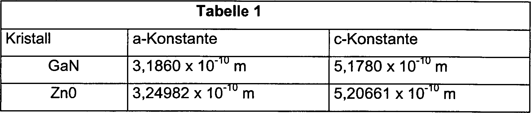
Ein Gitterversatz von 2% ist zwischen der auf dem Si-Substrat gebildeten ZnO-Pufferlage und der GaN-Lage immer noch vorhanden, wie die Tabelle 1 zeigt, obwohl diese 2% kleiner sind als in einer Kombination von GaN mit einem C-Ebenen-Saphirsubstrat oder einem SiC-Substrat. Deshalb bleiben immer noch die durch diesen Gitterversatz hervorgerufenen Kristallfehler.On Lattice offset of 2% is between that formed on the Si substrate ZnO buffer layer and the GaN layer is still present, as shown in Table 1, though these are 2% smaller than in a combination of GaN with one C-plane sapphire substrate or an SiC substrate. Therefore stay still the crystal defects caused by this lattice offset.
S. Srivastav, CVR Vasant Kumar and A. Mansingh: Effekt of oxygen on the physical parameters of RF sputtered ZnO thin film, J. Phys. D.: Appl. Phys. 22 (1989), Seiten 1768 bis 1772 beschreibt die Vergrößerung der Gitterkonstanten in a- und c-Richtung durch den Einbau von Sauerstoff auf Zwischengitterplätzen von ZnO-Filmen durch Einstellen der Prozeßparameter.S. Srivastav, CVR Vasant Kumar and A. Mansingh: Effect of oxygen on the physical parameters of RF sputtered ZnO thin film, J. Phys. D .: Appl. Phys. 22 (1989), pages 1768 to 1772 describes the enlargement of the Lattice constants in the a and c directions due to the incorporation of oxygen on interstitial spaces ZnO films by setting the process parameters.
Es ist die Aufgabe der vorliegenden Erfindung, die oben beschriebenen technischen Schwierigkeiten zu überwinden.It is the object of the present invention described above overcome technical difficulties.
Diese Aufgabe wird mit einem Verfahren zur Herstellung einer optoelektronischen Halbleitervorrichtung mit den Merkmalen des Anspruches 1 gelöst. Die Unteransprüche sind auf vorteilhafte Ausgestaltungen gerichtet.This The object is achieved with a method for producing an optoelectronic Semiconductor device with the features of claim 1 solved. The under claims are directed to advantageous embodiments.
Das erfindungsgemäße Verfahren bildet einen ZnO-Film auf einem Substrat, indem die Gitterkonstante in a-Achsenrichtung dieses ZnO-Films durch die Gitterkonstante des ZnO-Films in c-Achsenrichtung gesteuert oder geregelt wird.The inventive method forms a ZnO film on a substrate by adding the lattice constant in the a-axis direction of this ZnO film by the lattice constant of ZnO film is controlled or regulated in the c-axis direction.
Die ZnO-Pufferlage hat vorzugsweise eine Gitterkonstante von annähernd 5,2070·10–10 m oder größer. in Richtung der c-Achse.The ZnO buffer layer preferably has a lattice constant of approximately 5.2070 · 10 -10 m or greater. in the direction of the c-axis.
Es ist zu bevorzugen, daß die ZnO-Pufferlage eine Gitterkonstante von etwa 5,21 bis 5,28·10–10 m in Richtung der c-Achse und eine Gitterkonstante in a-Achsenrichtung von annähernd 3,24 bis 3,17·10–10 m hat.It is preferable that the ZnO buffer layer have a lattice constant of about 5.21 to 5.28 · 10 -10 m in the c-axis direction and a lattice constant in the a-axis direction of approximately 3.24 to 3.17 · 10 Has -10 m.
Um die Erfindung zu veranschaulichen, sind in den Zeichnungsfiguren einige bevorzugte Ausführungsbeispiele dargestellt, jedoch sollten diese so verstanden werden, dass die Erfindung nicht auf die dargestellten genaueren Anordnungen und Vorrichtungen beschränkt ist.Around the invention is illustrated in the drawing figures some preferred embodiments shown, however, these should be understood so that the Invention not based on the illustrated arrangements and Devices limited is.
Eine direkte Steuerung der Gitterkonstanten des auf einem Silicium- oder Glassubstrat abgeschiedenen ZnO-Films in Richtung der a-Achse hat sich wegen den Auswirkungen der Gitterkonstanten des Substrats als schwierig herausgestellt. Bei dem erfindungsgemäßen Verfahren zur Bildung eines ZnO-Films kann die Gitterkonstante des ZnO-Films in a-Achsenrichtung durch die Gitterkonstante des ZnO-Films in c-Achsenrichtung gesteuert werden. Die Gitterkonstante des ZnO-Films in c-Achsenrichtung läßt sich wiederum durch eine Steuerung oder Regelung von Parametern bei der Abscheidung des ZnO-Films einstellen.A direct control of the lattice constants on a silicon or Glass substrate deposited ZnO film in the direction of the a-axis itself because of the effects of the lattice constants of the substrate difficult exposed. In the inventive method for forming a ZnO film can be the lattice constant of the ZnO film in the a-axis direction controlled by the lattice constant of the ZnO film in the c-axis direction become. The lattice constant of the ZnO film in the c-axis direction can be again by controlling parameters in the Adjust deposition of the ZnO film.
Dieses Verfahren läßt sich bei der Herstellung einer Halbleiterphotonikvorrichtung anwenden, die eine durch InxGayAlzN dargestellte Halbleiterverbindung verwendet, worin x + y + z = 1, 0 ≤ x ≤ 1, 0 ≤ y ≤ 1 und 0 ≤ z ≤ 1 sind. Wenn die Gitterkonstante in a-Achsenrichtung der auf einer ZnO-Pufferlage gebildeten Halbleiterverbindung kleiner als die Gitterkonstante eines ZnO-Einkristalls in a-Achsenrichtung ist, kann die Gitterkonstante einer ZnO-Pufferlage in c-Achsenrichtung so eingestellt werden, dass sie größer ist als die Gitterkonstante des ZnO-Einkristalls in c-Achsenrichtung. Im Gegensatz kann die Gitterkonstante der ZnO-Pufferlage in c-Achsenrichtung so eingestellt werden, dass sie kleiner als die Gitterkonstante des ZnO-Einkristalls in c-Achsenrichtung ist, wenn die Gitterkonstante der auf der ZnO-Pufferlage gebildeten Halbleiter verbindung in a-Achsenrichtung größer als die Gitterkonstante des ZnO-Einkristalls in a-Achsenrichtung ist. Da die Gitterkonstante der ZnO-Pufferlage in a-Achsenrichtung annähernd gleich der Gitterkonstanten der Halbleiterverbindung in a-Achsenrichtung ist, kann eine Halbleiterverbindung mit hoher Kristallinität auf der ZnO-Pufferlage gebildet werden.This method can be applied to the manufacture of a semiconductor photonic device using a semiconductor compound represented by In x Ga y Al z N, where x + y + z = 1.0, ≤ x 1 1, 0 y y 1 1 and 0 z z ≤ 1 are. If the lattice constant in the a-axis direction of the semiconductor compound formed on a ZnO buffer layer is smaller than the lattice constant of a ZnO single crystal in the a-axis direction, the lattice constant of a ZnO buffer layer in the c-axis direction can be set to be larger than that Lattice constant of the ZnO single crystal in the c-axis direction. In contrast, the lattice constant of the ZnO buffer layer in the c-axis direction can be set to be smaller than the lattice constant of the ZnO single crystal in the c-axis direction when the lattice constant of the semiconductor compound formed on the ZnO buffer layer is larger in the a-axis direction than the lattice constant of the ZnO single crystal in the a-axis direction. Since the lattice constant of the ZnO buffer layer in the a-axis direction is approximately equal to the lattice constant of the semiconductor compound in the a-axis direction, a semiconductor compound with high crystallinity can be formed on the ZnO buffer layer.
Als eine aktuelle Anwendung wird bei einer Halbleiterphotonikvorrichtung auf einem Substrat eine ZnO-Pufferlage, die in c-Achsenrichtung eine Gitterkonstante von 5,2070 × 10⁻¹⁰ m oder mehr hat, und eine GaN-Lage auf der ZnO-Pufferlage gebildet, wobei die Halbleiterphotonikvorrichtung eine Halbleiterverbindung verwendet, die durch InxGayAlzN dargestellt ist, worin x + y + z = 1, 0 ≤ x ≤ 1, 0 ≤ y ≤ 1 und 0 ≤ z ≤ 1 sind.As a current application, a ZnO buffer layer having a lattice constant of 5.2070 × 10 -10 m or more in the c-axis direction and a GaN layer are formed on the ZnO buffer layer on a substrate in a semiconductor photonic device, the The semiconductor photonic device uses a semiconductor compound represented by In x Ga y Al z N, where x + y + z = 1, 0 ≤ x ≤ 1, 0 ≤ y ≤ 1 and 0 ≤ z ≤ 1.
Wenn die Gitterkonstante der ZnO-Pufferlage in c-Achsenrichtung so gesteuert wird, dass sie annähernd 5,2070 × 10⁻¹⁰ m oder mehr beträgt, kann die Gitterkonstante der ZnO-Pufferlage in a-Achsenrichtung gesteuert werden, dass sie kleiner ist als die Gitterkonstante des ZnO-Einkristalls in a-Achsenrichtung. Da der Unterschied zwischen der Gitterkonstanten der ZnO-Pufferlage in a-Achsenrichtung und der Gitterkonstanten der GaN-Lage im Vergleich mit den bekannten Verfahren verringert werden kann, kann auch der Gitterversatz zwischen der ZnO-Pufferlage und der GaN-Lage verringert werden.If the lattice constant of the ZnO buffer layer in the c-axis direction is controlled to be approximately 5.2070 × 10 -10 m or more, the lattice constant of the ZnO buffer layer in the a-axis direction can be controlled to be smaller than that Lattice constant of the ZnO single crystal in the a-axis direction. Since the difference between the lattice constant of the ZnO buffer layer in the a-axis direction and the lattice constant of the GaN layer can be reduced in comparison with the known methods, the lattice offset between the ZnO buffer layer and the GaN layer can also be reduced.
Wenn die Gitterkonstante der ZnO-Pufferlage in c-Achsenrichtung in einem Bereich von annähernd 5,21 bis 5,28 × 10⁻¹⁰ m liegt, wird die Gitterkonstante in a-Achsenrichtung gesteuert, dass sie in einem Bereich von annähernd 3,24 bis 3,17 × 10⁻¹⁰ m und damit näher an der Gitterkonstanten der GaN-Lage liegt.When the lattice constant of the ZnO buffer layer in the c-axis direction is in a range of approximately 5.21 to 5.28 × 10 -10 m, the lattice constant in the a-axis direction is controlled to be in a range of approximately 3.24 to 3.17 × 10 -10 m and thus closer to the lattice constant of the GaN layer.
In
solch einer Halbleiterphotonikvorrichtung
Die
ZnO-Pufferlage
Das
Ar-Gas und das O2-Gas werden mit vorgegebenen
Strömungsraten
der Kammer
Da
die a-Konstante und die c-Konstante des ZnO-Einkristalls jeweils
3,24982 × 10⁻¹⁰ m
und 5,20661 × 10⁻¹⁰ m
sind (in
Die
in
Die
Beziehung zwischen der c-Konstanten und der a-Konstanten der ZnO-Pufferlage bleibt
unverändert,
obwohl die Beziehung zwischen der c-Konstanten der ZnO-Pufferlage
Diese
Erfindung läßt sich
auch bei anderen Vorrichtungen anwenden, die keine Halbleiterphotonikvorrichtung
mit der Doppel-Heteroübergangsstruktur
der InGaN-Lage
Die
Vorrichtung kann eine Halbleiterphotonikvorrichtung
Obwohl
in den oben beschriebenen Beispielen GaN auf einem ZnO-Film gebildet
wird, läßt sich
diese Erfindung auch bei Fällen
anwenden, bei denen InGaN, InAlGaN oder AlGaN direkt auf einem ZnO-Film
abgeschieden wird. Z. B. kann übereinstimmend
mit der in
Da
die a-Konstante von Al0,2Ga0,8N
annähernd
3,176 × 10–10 m
ist, was sich aus der in
Weil
die a-Konstante von In0,2Al0,2Ga0,6N annähernd
3,245 × 10–10 m
ist, was sich aus der in
Claims (3)
Applications Claiming Priority (2)
| Application Number | Priority Date | Filing Date | Title |
|---|---|---|---|
| JP20512598A JP3522114B2 (en) | 1998-07-21 | 1998-07-21 | Semiconductor light emitting device, method of manufacturing the same, and method of forming ZnO film |
| JP10-205125 | 1998-07-21 |
Publications (2)
| Publication Number | Publication Date |
|---|---|
| DE19933552A1 DE19933552A1 (en) | 2000-02-03 |
| DE19933552B4 true DE19933552B4 (en) | 2004-12-02 |
Family
ID=16501851
Family Applications (1)
| Application Number | Title | Priority Date | Filing Date |
|---|---|---|---|
| DE19933552A Expired - Fee Related DE19933552B4 (en) | 1998-07-21 | 1999-07-16 | Method for producing an optoelectronic semiconductor device with a ZnO buffer layer |
Country Status (3)
| Country | Link |
|---|---|
| US (1) | US6291258B2 (en) |
| JP (1) | JP3522114B2 (en) |
| DE (1) | DE19933552B4 (en) |
Families Citing this family (16)
| Publication number | Priority date | Publication date | Assignee | Title |
|---|---|---|---|---|
| JPH11274467A (en) * | 1998-03-26 | 1999-10-08 | Murata Mfg Co Ltd | Photo-electronic integrated-circuit device |
| JP4438024B2 (en) * | 1999-04-28 | 2010-03-24 | キヤノン株式会社 | Inspection method of semiconductor laser device |
| US6448584B1 (en) * | 2000-01-14 | 2002-09-10 | Shih-Hsiung Chan | Light emitting diode with high luminance and method for making the same |
| JP2001244547A (en) * | 2000-03-01 | 2001-09-07 | Canon Inc | Semiconductor laser and observing method for light emitting part of semiconductor laser |
| KR20010000545A (en) * | 2000-10-05 | 2001-01-05 | 유태경 | The multiple wavelength AlGaInN LED device with pumping layer |
| US8618595B2 (en) * | 2001-07-02 | 2013-12-31 | Merck Patent Gmbh | Applications of light-emitting nanoparticles |
| US6918946B2 (en) * | 2001-07-02 | 2005-07-19 | Board Of Regents, The University Of Texas System | Applications of light-emitting nanoparticles |
| US6846565B2 (en) | 2001-07-02 | 2005-01-25 | Board Of Regents, The University Of Texas System | Light-emitting nanoparticles and method of making same |
| JP4817350B2 (en) * | 2001-07-19 | 2011-11-16 | 株式会社 東北テクノアーチ | Method for producing zinc oxide semiconductor member |
| JP3749498B2 (en) * | 2002-03-26 | 2006-03-01 | スタンレー電気株式会社 | Crystal growth substrate and ZnO-based compound semiconductor device |
| KR101319512B1 (en) | 2005-05-02 | 2013-10-21 | 니치아 카가쿠 고교 가부시키가이샤 | Nitride based semiconductor element and method for fabricating the same |
| US7906415B2 (en) * | 2006-07-28 | 2011-03-15 | Xerox Corporation | Device having zinc oxide semiconductor and indium/zinc electrode |
| TW200839960A (en) * | 2007-03-22 | 2008-10-01 | Univ Nat Sun Yat Sen | Structure of ZnO buffer layer and fabrication method thereof |
| US8217498B2 (en) * | 2007-10-18 | 2012-07-10 | Corning Incorporated | Gallium nitride semiconductor device on SOI and process for making same |
| US20090272975A1 (en) * | 2008-05-05 | 2009-11-05 | Ding-Yuan Chen | Poly-Crystalline Layer Structure for Light-Emitting Diodes |
| US8642369B2 (en) * | 2009-03-03 | 2014-02-04 | Zn Technology, Inc. | Vertically structured LED by integrating nitride semiconductors with Zn(Mg,Cd,Be)O(S,Se) and method for making same |
Citations (3)
| Publication number | Priority date | Publication date | Assignee | Title |
|---|---|---|---|---|
| DE19629720A1 (en) * | 1995-07-27 | 1997-02-13 | Nec Corp | Semiconductor light emitting device and manufacturing method therefor |
| DE19648955A1 (en) * | 1995-11-27 | 1997-05-28 | Sumitomo Chemical Co | III=V compound semiconductor device, e.g. blue light LED or laser diode |
| US5679965A (en) * | 1995-03-29 | 1997-10-21 | North Carolina State University | Integrated heterostructures of Group III-V nitride semiconductor materials including epitaxial ohmic contact, non-nitride buffer layer and methods of fabricating same |
Family Cites Families (4)
| Publication number | Priority date | Publication date | Assignee | Title |
|---|---|---|---|---|
| JP3974667B2 (en) | 1994-08-22 | 2007-09-12 | ローム株式会社 | Manufacturing method of semiconductor light emitting device |
| JPH08139361A (en) | 1994-11-08 | 1996-05-31 | Toshiba Corp | Compound semiconductor light emitting device |
| JPH10173228A (en) | 1996-12-09 | 1998-06-26 | Ricoh Co Ltd | Compound semiconductor substrate and semiconductor light-emitting element |
| JPH10178202A (en) | 1996-12-18 | 1998-06-30 | Mitsubishi Cable Ind Ltd | Manufacture of gan-based substrate |
-
1998
- 1998-07-21 JP JP20512598A patent/JP3522114B2/en not_active Expired - Fee Related
-
1999
- 1999-07-16 DE DE19933552A patent/DE19933552B4/en not_active Expired - Fee Related
-
2001
- 2001-01-02 US US09/753,590 patent/US6291258B2/en not_active Expired - Lifetime
Patent Citations (3)
| Publication number | Priority date | Publication date | Assignee | Title |
|---|---|---|---|---|
| US5679965A (en) * | 1995-03-29 | 1997-10-21 | North Carolina State University | Integrated heterostructures of Group III-V nitride semiconductor materials including epitaxial ohmic contact, non-nitride buffer layer and methods of fabricating same |
| DE19629720A1 (en) * | 1995-07-27 | 1997-02-13 | Nec Corp | Semiconductor light emitting device and manufacturing method therefor |
| DE19648955A1 (en) * | 1995-11-27 | 1997-05-28 | Sumitomo Chemical Co | III=V compound semiconductor device, e.g. blue light LED or laser diode |
Non-Patent Citations (4)
| Title |
|---|
| DE-B.: Gerthsen, Kneser, Vogel, "Physik", 14. Aufl., Springer-Verlag Berlin, 1982, ISBN 3-540113 11369-X S. 112-113 |
| DE-B.: Gerthsen, Kneser, Vogel, "Physik", 14. Aufl., Springer-Verlag Berlin, 1982, ISBN 3-54011311369-X S. 112-113 * |
| S.Srivalav et al: Effect of oxgen on the physical paramters of RF sputtered ZuO thinfilm. In:J.Phys. D: Appl. Phys. 22(1989), S.1768-1772 |
| S.Srivalav et al: Effect of oxgen on the physical paramters of RF sputtered ZuO thinfilm. In:J.Phys.D: Appl. Phys. 22(1989), S.1768-1772 * |
Also Published As
| Publication number | Publication date |
|---|---|
| JP3522114B2 (en) | 2004-04-26 |
| DE19933552A1 (en) | 2000-02-03 |
| US20010000916A1 (en) | 2001-05-10 |
| US6291258B2 (en) | 2001-09-18 |
| JP2000036617A (en) | 2000-02-02 |
Similar Documents
| Publication | Publication Date | Title |
|---|---|---|
| DE19933552B4 (en) | Method for producing an optoelectronic semiconductor device with a ZnO buffer layer | |
| DE60217943T2 (en) | A nitride semiconductor device and method of making the same | |
| DE19734034C2 (en) | Epitaxial wafer for light emitting device, method of forming the wafer and light emitting device using the wafer | |
| DE60317862T2 (en) | Light-emitting semiconductor device | |
| DE60121768T2 (en) | METHOD FOR PRODUCING A SEMICONDUCTOR COMPONENT WITH NITRIDE COMPOSITION OF GROUP III | |
| DE60128134T2 (en) | GALLIUM NITRIDE MATERIALS AND METHOD FOR PRODUCING LAYERS OF THIS MATERIAL | |
| DE69333829T2 (en) | Light-emitting device based on a gallium nitride semiconductor compound | |
| DE69533276T2 (en) | Semiconductor light-emitting devices | |
| DE10213395B4 (en) | Indium gallium nitride smoothing structures for III-nitride arrangements | |
| DE19680872B4 (en) | Method for producing a light-emitting element | |
| DE112007002182B4 (en) | Method of manufacturing a group III nitride compound semiconductor light emitting device | |
| DE112005000296B4 (en) | Gallium nitride compound semiconductor multilayer structure, lamp with it and manufacturing method for it | |
| DE102007027446B4 (en) | Group III-V nitride-based semiconductor substrate and Group III-V nitride-based light emitting device | |
| DE19941875C2 (en) | Optoelectronic semiconductor device | |
| DE10253082A1 (en) | Semiconductor light emitter and photodetector based on gallium nitride | |
| DE19715572A1 (en) | Selective epitaxy of III-V nitride semiconductor layers | |
| DE60014097T2 (en) | NITRID SEMICONDUCTOR LAYER STRUCTURE AND THEIR APPLICATION IN SEMICONDUCTOR LASERS | |
| DE112005002133T5 (en) | Layer stack structure with N-type Group III nitride semiconductors | |
| DE112006001084T5 (en) | Light-emitting devices having active layers extending into open dimples | |
| DE112015000824B4 (en) | Method for manufacturing an electronic semiconductor chip | |
| DE10330629A1 (en) | Epitaxial substrate for light-emitting compound semiconductor device, method for its production and light-emitting device | |
| DE19855476A1 (en) | Gallium nitride based semiconductor layer is formed by electron cyclotron resonance molecular beam epitaxy | |
| DE112004002804B4 (en) | Growth method for thin In-rich nitride semiconductor layer and UV light-emitting device with In-rich nitride semiconductor layer | |
| DE19882202B4 (en) | Semiconductor light-emitting device and method for its production | |
| DE19603782A1 (en) | Layered III=V semiconductor structure |
Legal Events
| Date | Code | Title | Description |
|---|---|---|---|
| OP8 | Request for examination as to paragraph 44 patent law | ||
| 8364 | No opposition during term of opposition | ||
| R119 | Application deemed withdrawn, or ip right lapsed, due to non-payment of renewal fee |