DE10253717B4 - Device for contacting for the test of at least one test object, test system and method for testing test objects - Google Patents
Device for contacting for the test of at least one test object, test system and method for testing test objects Download PDFInfo
- Publication number
- DE10253717B4 DE10253717B4 DE10253717A DE10253717A DE10253717B4 DE 10253717 B4 DE10253717 B4 DE 10253717B4 DE 10253717 A DE10253717 A DE 10253717A DE 10253717 A DE10253717 A DE 10253717A DE 10253717 B4 DE10253717 B4 DE 10253717B4
- Authority
- DE
- Germany
- Prior art keywords
- test
- substrate
- contacting
- unit
- optical axis
- Prior art date
- Legal status (The legal status is an assumption and is not a legal conclusion. Google has not performed a legal analysis and makes no representation as to the accuracy of the status listed.)
- Expired - Fee Related
Links
Images


Classifications
-
- G—PHYSICS
- G01—MEASURING; TESTING
- G01R—MEASURING ELECTRIC VARIABLES; MEASURING MAGNETIC VARIABLES
- G01R31/00—Arrangements for testing electric properties; Arrangements for locating electric faults; Arrangements for electrical testing characterised by what is being tested not provided for elsewhere
- G01R31/28—Testing of electronic circuits, e.g. by signal tracer
- G01R31/302—Contactless testing
- G01R31/305—Contactless testing using electron beams
-
- G—PHYSICS
- G09—EDUCATION; CRYPTOGRAPHY; DISPLAY; ADVERTISING; SEALS
- G09G—ARRANGEMENTS OR CIRCUITS FOR CONTROL OF INDICATING DEVICES USING STATIC MEANS TO PRESENT VARIABLE INFORMATION
- G09G3/00—Control arrangements or circuits, of interest only in connection with visual indicators other than cathode-ray tubes
- G09G3/006—Electronic inspection or testing of displays and display drivers, e.g. of LED or LCD displays
-
- G—PHYSICS
- G01—MEASURING; TESTING
- G01R—MEASURING ELECTRIC VARIABLES; MEASURING MAGNETIC VARIABLES
- G01R31/00—Arrangements for testing electric properties; Arrangements for locating electric faults; Arrangements for electrical testing characterised by what is being tested not provided for elsewhere
- G01R31/28—Testing of electronic circuits, e.g. by signal tracer
- G01R31/2851—Testing of integrated circuits [IC]
- G01R31/2886—Features relating to contacting the IC under test, e.g. probe heads; chucks
- G01R31/2887—Features relating to contacting the IC under test, e.g. probe heads; chucks involving moving the probe head or the IC under test; docking stations
-
- G—PHYSICS
- G01—MEASURING; TESTING
- G01R—MEASURING ELECTRIC VARIABLES; MEASURING MAGNETIC VARIABLES
- G01R31/00—Arrangements for testing electric properties; Arrangements for locating electric faults; Arrangements for electrical testing characterised by what is being tested not provided for elsewhere
- G01R31/28—Testing of electronic circuits, e.g. by signal tracer
- G01R31/302—Contactless testing
Landscapes
- Engineering & Computer Science (AREA)
- Physics & Mathematics (AREA)
- General Physics & Mathematics (AREA)
- General Engineering & Computer Science (AREA)
- Computer Hardware Design (AREA)
- Theoretical Computer Science (AREA)
- Microelectronics & Electronic Packaging (AREA)
- Tests Of Electronic Circuits (AREA)
Abstract
Verfahren zum Testen von Testobjekten auf einem Substrat (140) mit mehreren Testobjekten (301; 401), wobei zum Testen eine Testvorrichtung mit einer optischen Achse (102) und einem zur optischen Achse zugehörigen Test-Bereich verwendet wird, mit folgenden Schritten:
– legen des Substrats auf einen Halter (130);
– kontaktieren eines ersten Testobjekts mit einer Kontaktiereinheit (150) welche maximal die Abmessung der halben Halterabmessung in einer Richtung senkrecht zu der optischen Achse aufweist;
– positionieren des Substrats (140) und der optischen Achse (102) relativ zueinander, so dass ein erster Bereich (303) des ersten Testobjekts in dem Test-Bereich (302) der Testvorrichtung liegt;
– testen des ersten Bereiches des Testobjektes;
– verschieben des Substrates und der optischen Achse relativ zueinander, so dass mindestens ein weiterer Bereich (304) des ersten Testobjektes in dem Test-Bereich der Testvorrichtung liegt, wobei die Kontaktiereinheit verschoben wird, so dass die Position der Kontaktiereinheit in Bezug auf das...A method of testing test objects on a substrate (140) having a plurality of test objects (301; 401) using a test device having an optical axis (102) and a test area associated with the optical axis for testing, comprising the steps of:
Placing the substrate on a holder (130);
- Contacting a first test object with a contacting unit (150) which has a maximum of the dimension of the half holder dimension in a direction perpendicular to the optical axis;
- positioning the substrate (140) and the optical axis (102) relative to one another such that a first region (303) of the first test object lies within the test area (302) of the test device;
- test the first area of the test object;
Moving the substrate and the optical axis relative to each other such that at least one further area (304) of the first test object lies in the test area of the test device, wherein the contact unit is displaced, so that the position of the contact unit with respect to the .. ,

Description
Die Erfindung bezieht sich auf das Testen von großen Flächen. Dabei werden als Testmethode insbesondere Tests mit einem Korpuskularstrahl eingesetzt. Die vorliegende Erfindung bezieht sich insbesondere auf die Kontaktierung von Testobjekten. Im Speziellen bezieht sich die vorliegende Erfindung auf ein Verfahren zum Positionieren und Kontaktieren eines Substrats, auf ein Verfahren zum Testen eines Substrats, auf eine Vorrichtung zum Kontaktieren für den Test von mindestens einem Testobjekt und auf ein Test-System.The invention relates to the testing of large areas. In particular, tests with a corpuscular beam are used as the test method. The present invention relates in particular to the contacting of test objects. More particularly, the present invention relates to a method of positioning and contacting a substrate, to a method of testing a substrate, to a device for contacting for testing at least one test object, and to a test system.
Mit steigender Nachfrage für Bildschirmelemente ohne Bildröhre wachsen die Anforderungen für Flüssigkristallanzeigen (LCD) und andere Anzeigeelemente, bei denen Schaltelemente wie zum Beispiel Dünnfilmtransistoren (TFT) verwendet werden. Bei diesen Anzeigeelementen sind die Bildpunkte, die sogenannten Pixel, matrixförmig angeordnet.As the demand for non-CRT screen elements increases, the demands for liquid crystal displays (LCD) and other display elements using switching elements such as thin film transistors (TFTs) are growing. In these display elements, the pixels, the so-called pixels, are arranged in a matrix.
Aber auch in anderen Bereichen muss eine zunehmende Zahl von Elementen getestet werden. Hierbei kann es sich zum Beispiel um mikroelektronische und/oder mikromechanische Elemente handeln. Hierzu zählen beispielweise Dünnschichttransistoren, Verbindungsnetzwerke eines Chips, Transistoren, Elektronenemitter eines Emitterarrays, Elektroden für Bildpixel eines Displays, mikromechanische Spiegel eines Arrays und andere Elemente, die sich insbesondere dadurch auszeichnen, dass es sich um eine Vielzahl von Elementen handelt (100.000 bis mehrerer 1.000.000), wobei jedes Element für sich elektrisch ansteuerbar ist.But also in other areas an increasing number of elements has to be tested. These may be, for example, microelectronic and / or micromechanical elements. These include, for example, thin-film transistors, interconnection networks of a chip, transistors, electron emitter of an emitter array, electrodes for image pixels of a display, micromechanical mirrors of an array and other elements, which are characterized in that they are a plurality of elements (100,000 to several 1,000. 000), each element being electrically controllable by itself.
Zum Beispiel offenbart
Um zum Beispiel eine gute Bildqualität von Anzeigeelementen zu erhalten, dürfen nur sehr wenige der mehrere Millionen Pixel defekt sein. Zur Gewährleistung einer kostengünstigen Produktion ist es daher vor allem für die immer größer werdenden Anzeigeelemente wichtig, leistungsfähige Online-Testverfahren zur Verfügung zustellen. Ein solches Testverfahren ist beispielweise in der Druckschrift
Bei solchen Testverfahren werden Kontaktiereinheiten verwendet, die zum einen einen Signalaustausch zu externen Geräten zulassen und zum anderen eine Abtastung durch einen Elektronenstrahl erlauben. Dabei existieren gemäß dem Stand der Technik verschiedene Lösungen.In such test methods contacting units are used, which allow on the one hand a signal exchange to external devices and on the other hand allow scanning by an electron beam. There are different solutions according to the prior art.
Werden Displays getestet, so kann um die Fläche eines Displays ein Rahmen angeordnet werden, der elektrische Kontakte zu dem Display herstellt. Auf einem Substrat sind in der Regel mehrere Displays angeordnet. Da durch den beschränkten Messbereich eines Elektronenstrahlsystems jeweils nur ein Display getestet werden kann, wird für den Test eines weiteren Displays der Kontaktrahmen angehoben, das Substrat verschoben und der Kontaktrahmen auf das nächste Display aufgesetzt. Mit einer solchen Anordnung können jedoch nur Displays getestet werden, deren ganze Fläche durch Scannen des Korpuskularstrahls abgedeckt werden kann.If displays are tested, a frame can be arranged around the surface of a display, which produces electrical contacts to the display. On a substrate usually several displays are arranged. Since only one display can be tested in each case due to the limited measuring range of an electron beam system, the contact frame is raised for the test of another display, the substrate is displaced and the contact frame is placed on the next display. With such an arrangement, however, only displays can be tested whose entire surface can be covered by scanning the corpuscular beam.
Darüber hinaus gibt es Kontaktrahmen, die alle Displays auf einem Glassubstrat gleichzeitig kontaktiren. Ein solcher Kontaktrahmen wird mit dem Substrat verschoben, wenn andere Displays getestet werden sollen.In addition, there are contact frames that simultaneously contact all displays on a glass substrate. Such a contact frame is displaced with the substrate when other displays are to be tested.
Ein Nachteil solcher Kontaktrahmen für das gesamte Substrat ist, dass bei wechselnden Displaygrößen der gesamte Kontaktrahmen ausgetauscht werden muss. Aus diesem Grund muss das System bei wechselnden Chargen belüftet werden, was die Produktivität verringern. Darüber hinaus müssen die Kontaktrahmen für unterschiedliche Displaytypen und Displaygrößen gelagert werden, um bei Bedarf eingesetzt werden zu können.A disadvantage of such contact frames for the entire substrate is that with changing display sizes of the entire contact frame must be replaced. For this reason, the system must be ventilated with changing batches, which reduces productivity. In addition, the contact frames for different display types and display sizes must be stored in order to be used if necessary.
Die Aufgabe der Erfindung ist es, die Probleme des Standes der Technik zumindest teilweise zu mindern. Insbesondere soll die Möglichkeit bestehen bei einem Test unterschiedliche Testobjekte mit unterschiedlichen Abmessungen von Testobjekten mit einer Vorrichtung zu testen.The object of the invention is to at least partially alleviate the problems of the prior art. In particular, it should be possible in a test to test different test objects with different dimensions of test objects with a device.
Dabei sind Testobjekte im Sinn der vorliegenden Erfindung zum Beispiel Displays, eine Gruppierung von Displays, Arrays anderer mikroelektronischer oder mikromechanischer Elemente, sowie einzelne Schaltungen, die zum Beispiel auf Kurzschlüsse oder fehlende Kontakte zwischen Bereichen der Schaltung getestet werden.For the purposes of the present invention, test objects are, for example, displays, a grouping of displays, arrays of other microelectronic or micromechanical elements, and individual circuits which are tested, for example, for short circuits or missing contacts between areas of the circuit.
Die Aufgabe wird gelöst durch die Gegenstände der Ansprüche 1, 15, 16, und 31.The object is solved by the subject matters of
Bevorzugte Ausführungen und besondere Aspekte der Erfindung ergeben sich aus den Unteransprüchen. Preferred embodiments and particular aspects of the invention will become apparent from the dependent claims.
Gemäß einem Aspekt wird die Aufgabe der vorliegenden Erfindung gelöst durch ein Verfahren zum Testen von Testobjekten auf einem Substrat mit mehreren Testobjekten, wobei zum Testen eine Testvorrichtung mit einer optischen Achse und einem zugehörigen Testbereich verwendet wird. Das Verfahren enthält legen des Substrats auf einen Halter, kontaktieren eines ersten Testobjekts mit einer Kontaktiereinheit welche maximal die Abmessung der halben Halterabmessung in einer Richtung senkrecht zu der optischen Achse aufweist, positionieren des Substrats und der optischen Achse relativ zueinander, so dass ein erster Bereich des ersten Testobjekts in dem Test-Bereich der Testvorrichtung liegt, testen des ersten Bereiches des Testobjektes, verschieben des Substrates und der optischen Achse relativ zueinander, so dass mindestens ein weiterer Bereich des ersten Testobjektes in dem Test-Bereich der Testvorrichtung liegt wobei die Kontaktiereinheit verschoben wird, so dass die Position der Kontaktiereinheit in Bezug auf das erste Testobjekt im wesentlichen unverändert ist, testen des weiteren Bereiches des Testobjektes, verschieben der Kontaktiereinheit und des Substrats relativ zueinander, so dass ein weiteres Testobjekt kontaktiert werden kann.According to one aspect, the object of the present invention is achieved by a method for testing test objects on a substrate with a plurality of test objects, wherein a test device having an optical axis and an associated test area is used for testing. The method includes placing the substrate on a holder, contacting a first device under test with a contactor unit having a maximum dimension of half the holder dimension in a direction perpendicular to the optical axis, positioning the substrate and the optical axis relative to each other, such that a first portion of the first test object in the test area of the test device, testing the first area of the test object, moving the substrate and the optical axis relative to each other, so that at least one further area of the first test object lies in the test area of the test device, wherein the contact unit is displaced such that the position of the contacting unit with respect to the first test object is essentially unchanged, testing the further area of the test object, displacing the contacting unit and the substrate relative to one another so that a further test object can be contacted.
Durch die oben beschriebenen Aspekte der vorliegenden Erfindung wird eine Kontaktierung unterschiedlich gestalteter Testobjekte ermöglicht, ohne dass ein Austausch der Kontaktiereinheit notwendig ist. Darüber hinaus ist es möglich, Testobjekte mit der Testvorrichtung zu prüfen, deren Größe den Test-Bereich der Testvorrichtung überschreitet. Als Testvorrichtung werden in diesem Zusammenhang die Komponenten zur Erzeugung des Messsignals verstanden. Diese sind: eine Quelle für die Erzeugung eines primären Korpuskularstrahls, Strahlformungs- und Strahlablenkungskomponenten zur Lenkung des Strahls auf eine Fläche, die zur Gewinnung des Messsignals genutzt wird, Komponenten zur Lenkung und/oder Abbildung eines Messsignals auf eine Detektoreinheit und die Detektoreinheit.By the above-described aspects of the present invention, a contacting of differently shaped test objects is made possible without the need for replacement of the contacting unit. In addition, it is possible to test objects with the test device whose size exceeds the test range of the test device. In this context, the test device is understood to mean the components for generating the measurement signal. These are: a source for the generation of a primary particle beam, beam shaping and beam deflection components for directing the beam onto an area used to obtain the measurement signal, components for steering and / or imaging a measurement signal on a detector unit and the detector unit.
Im Rahmen der oben genannten Aspekte ist es insbesondere bevorzugt, wenn die Positionierung der Kontaktiereinheit über einen der Kontaktiereinheit zugeordneten Antrieb erfolgt. Dadurch kann die Kontaktiereinheit schnell und flexibel von einer Position zur nächsten Position bewegt werden. Dies erhöht die Testgeschwindigkeit für das gesamte Substrat und somit den Durchsatz des Testsystems.In the context of the above-mentioned aspects, it is particularly preferred if the positioning of the contacting unit takes place via a drive associated with the contacting unit. As a result, the contacting unit can be moved quickly and flexibly from one position to the next position. This increases the test speed for the entire substrate and thus the throughput of the test system.
Die erfindungsgemäße Aufgabe wird gemäß einem weiteren Aspekte gelost durch eine Vorrichtung zum Kontaktieren für den Test mindestens eines Testobjekts auf einem Substrat, wobei für den Test eine Testvorrichtung mit einer optischen Achse und einem zugehörigen Testbereich verwendet wird. Die Vorrichtung enthält einen Halter für ein Substrat mit mindestens einem Testobjekt, eine Verschiebeeinheit für den Halter, und eine Kontaktiereinheit zum Kontaktieren des mindestens einen Testobjektes, wobei die Kontaktiereinheit und die optische Achse relativ zueinander verschiebbar sind, wobei die Kontaktiereinheit unabhängig davon relativ zum Halter verschiebbar ist, und wobei die Kontaktiereinheit maximal die Abmessung der halben Halterabmessung in einer Richtung senkrecht zu der optischen Achse aufweist.The object according to the invention is achieved according to a further aspect by a device for contacting for the test of at least one test object on a substrate, wherein a test device having an optical axis and an associated test area is used for the test. The device includes a holder for a substrate with at least one test object, a displacement unit for the holder, and a contacting unit for contacting the at least one test object, wherein the contacting unit and the optical axis are displaceable relative to each other, the contacting unit being displaceable relative to the holder independently and wherein the contacting unit has at most the dimension of the half holder dimension in a direction perpendicular to the optical axis.
Gemäß einem weiteren Aspekt enthält die Vorrichtung einen Halter für ein Substrat mit mindestens einem Testobjekt, einer Verschiebeeinheit für eine Verschiebung der optischen Achse, und eine Kontaktiereinheit zum kontaktieren des mindestens einen Testobjektes, wobei die Kontaktiereinheit relativ zur optischen Achse und unabhängig davon relativ zum Halter verschiebbar ist und maximal die Abmessung der halben Halterabmessung in einer Richtung senkrecht zu einer optischen Achse aufweist.According to a further aspect, the device includes a holder for a substrate with at least one test object, an optical axis displacement unit, and a contact unit for contacting the at least one test object, the contact unit being displaceable relative to the optical axis and independently relative to the holder is and has at most the dimension of the half holder dimension in a direction perpendicular to an optical axis.
Ein prinzipieller Aspekt der Erfindung ist eine Vorrichtung zum Kontaktieren. Diese besteht aus einem Halter für ein Substrat und einer zugeordneten Verschiebeeinheit. Darüber hinaus existiert eine ebenfalls verschiebbare Kontaktiereinheit die zumindest in einer Richtung senkrecht zu einer optischen Achse eines Korpuskularstrahl-Testers maximal die halbe Ausdehnung des Halters in dieser Richtung hat.A principal aspect of the invention is a device for contacting. This consists of a holder for a substrate and an associated displacement unit. In addition, there is also a sliding contact unit which has at least one direction perpendicular to an optical axis of a particle beam tester a maximum of half the extent of the holder in this direction.
Hierbei ist es insbesondere bevorzugt, wenn die Kontaktiereinheit in beiden Richtungen senkrecht zur optischen Achse eines Korpuskularstrahl-Testers maximal die halbe Ausdehnung des Halters in diesen Richtungen hat.In this case, it is particularly preferred if the contacting unit has, in both directions perpendicular to the optical axis of a particle beam tester, a maximum of half the extent of the holder in these directions.
Die vorliegende Erfindung kann auch folgendermaßen formuliert werden. Die Aufgabe wird gemäß einem Aspekt der Erfindung gelöst durch eine Vorrichtung zum Kontaktieren innerhalb eines Testsystems. Das Testsystem enthält einen Halter, der relativ zur optischen Achse einer Testvorrichtung verschiebbar ist, und eine Kontaktiereinheit, die ebenfalls relativ zur optischen Achse verschiebbar ist. Die Kontaktiereinheit ist während des Testens des Substrats zusätzlich gegenüber dem Substrat verschiebbar.The present invention may also be formulated as follows. The object is achieved according to one aspect of the invention by a device for contacting within a test system. The test system includes a holder which is displaceable relative to the optical axis of a test device, and a contacting unit which is also displaceable relative to the optical axis. The contacting unit is additionally displaceable relative to the substrate during the testing of the substrate.
Im Bezug auf diesen Aspekt ist es zu bevorzugen, wenn die Kontaktiereinheit während des Testens der Testobjekte eines Substrats mindestens 10 cm, besonders bevorzugt mindestens 25 cm verschiebbar ist.With regard to this aspect, it is preferable if the contacting unit is displaceable during testing of the test objects of a substrate at least 10 cm, particularly preferably at least 25 cm.
Die erfindungsgemäße Aufgabe wird gemäß einem weiteren Aspekt durch ein Testsystem gelöst. Dieses Testsystem besteht aus einer Korpuskularstrahlsäule, einer Testkammer und einer Vorrichtung zum Kontaktieren von mindestens einem Testobjekt auf einem Substrat gemäß einem der oben genannten Aspekte. The object according to the invention is achieved according to a further aspect by a test system. This test system consists of a corpuscular beam column, a test chamber and a device for contacting at least one test object on a substrate according to one of the above-mentioned aspects.
Dabei ist es bevorzugt, wenn die Test-Kammer evakuierbar ist. Ferner ist es bevorzugt, wenn die Korpuskularstrahlsäule eine Elektronenstrahlsäule ist, wobei insbesondere ein Emitter, Ablenkungseinheiten und Strahlformungsoptiken innerhalb der Säule enthalten sind.It is preferred if the test chamber can be evacuated. Furthermore, it is preferred if the corpuscular beam column is an electron beam column, wherein in particular an emitter, deflection units and beam shaping optics are contained within the column.
Gemäß der vorliegenden Erfindung kann der Korpuskularstrahl auch durch Photonen gebildet werden, d. h. es wird ein lichtoptischer Test der Elemente der Testobjekte auf dem Substrat durchgeführt.According to the present invention, the corpuscular beam can also be formed by photons, i. H. a light-optical test of the elements of the test objects on the substrate is carried out.
Ferner ist es möglich, um den für eine Verschiebung des Glassubstrats benötigten Raum einzusparen, nicht das Glassubstrat und eine Kontaktiereinheit relativ zur optischen Achse einer Testvorrichtung zu bewegen, sondern das Glassubstrat ruhen zu lassen. In einem solchen Fall wird zum einen die optische Achse der Testvorrichtung relativ zum Glassubstrat bewegt. Zum anderen wird darüber hinaus die Kontaktiereinheit relativ zum Glassubstrat bewegt und die Kontaktiereinheit und die optische Achse der Testvorrichtung relativ zueinander bewegt.Further, in order to save space required for displacement of the glass substrate, it is not possible to move the glass substrate and a contacting unit relative to the optical axis of a test apparatus, but to rest the glass substrate. In such a case, on the one hand, the optical axis of the test device is moved relative to the glass substrate. On the other hand, moreover, the contacting unit is moved relative to the glass substrate and the contacting unit and the optical axis of the test apparatus are moved relative to each other.
Die Erfindung bezieht sich ferner auf Vorrichtungen, mit Merkmalen, die notwendig sind um die beschriebenen Verfahren durchzuführen. Darüber hinaus bezieht sich die Erfindung auf Methoden, die durch die Verwendung der beschriebenen Vorrichtungen charakterisiert werden.The invention further relates to devices having features necessary to perform the described methods. Moreover, the invention relates to methods characterized by the use of the devices described.
Ausführungsbeispiele der Erfindung sind in den Figuren dargestellt, und werden im folgenden exemplarisch näher beschrieben.Embodiments of the invention are illustrated in the figures, and will be described in more detail below by way of example.
Es zeigen:Show it:
Die vorliegende Erfindung kann mit einer Vielzahl von Testverfahren verwendet werden. Aus Gründen der Einfachheit wird die vorliegende Erfindung im folgenden zunächst durch das Testen von Bildschirmen mit einem Elektronenstrahl beschrieben.The present invention can be used with a variety of testing methods. For the sake of simplicity, the present invention will be described below first by testing screens with an electron beam.
Hierzu sollen anhand von
Zum Testen eines Displays wird der Elektronenstrahl mittels Deflektoren über das Glassubstrat gescannt. Dabei wird ein Bereich
Bild 9 zeigt ein Display
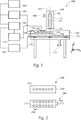
In der Regel müssen die Displays für Testverfahren elektronisch kontaktiert werden, um die Funktionalität der Displays zu testen. Hierzu wird auf das Glassubstrat eine Kontaktiereinheit
In Bezug auf
Die Anordnung
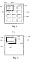
Das gesamte Glassubstrat ist zu groß, um ohne Verschiebung durch einen Elektronenstrahl getestet zu werden. Um eine Messung eines Bereiches eines Displays, der innerhalb des Test-Bereichs liegt, durchzuführen wird das Display
In
Zum Testen aller Displays auf dem Glassubstrat
Die
Die Anordnung
Wie man bei einem Vergleich von
Da das Belüften und die Evakuierung im Rahmen der laufenden Produktion mit großen Nachteilen verbunden ist, ist es wünschenswert solche Probleme durch die vorliegenden Erfindung zu verringern.Since venting and evacuation are associated with major drawbacks in current production, it is desirable to reduce such problems by the present invention.
Im Folgenden werden Ausführungsformen und bevorzugte Aspekte der vorliegenden Erfindung anhand der
Unter Korpuskularstrahl wird im Rahmen dieser Erfindung ein Strahl geladener Teilchen (Partikelstrahl), wie zum Beispiel ein Elektronen oder Ionenstrahl, oder ein Laserstrahl verstanden. Das bedeutet, es wird unter dem Begriff Korpuskularstrahl sowohl ein Laserstrahl, bei dem die Korpuskel Photonen sind, als auch ein Partikelstrahl, bei dem die Korpuskel Ionen, Atome, Elektronen oder andere Partikel sind, verstanden. Beispielhaft, wird im Folgenden auf einen Elektronenstrahl Bezug genommen.For the purposes of the present invention, a particle beam is understood to mean a beam of charged particles (particle beam), such as, for example, an electron or ion beam, or a laser beam. This means that the term "corpuscular beam" means both a laser beam in which the particles are photons and a particle beam in which the particles are ions, atoms, electrons or other particles. By way of example, reference will hereinafter be made to an electron beam.
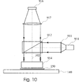
Darüber hinaus zeigt
Die Testkammer kann über den Vakuumflansch
Der Antrieb
Bezugnehmend auf
Für die Testverfahren wird der Elektronenstrahl auf ein Element eines Displays auf dem Substrat gerichtet. Dabei kann zum einen eine Aufladung von Bereichen des zu testenden Elements erzielt werden. Darüber hinaus können aber auch emittierte Sekundärelektronen mit einem Detektor (nicht dargestellt) gemessen werden. Durch die Messung der Sekundärelektronen können Potentialverteilungen auf dem Displays gemessen sowie durch andere Detektionsmethoden auch Topologien oder Materialzusammensetzungen bestimmt werden.For the test methods, the electron beam is directed to an element of a display on the substrate. In this case, on the one hand, charging of regions of the element to be tested can be achieved. In addition, however, emitted secondary electrons can also be measured with a detector (not shown). By measuring the secondary electrons, it is possible to measure potential distributions on the display and also to determine topologies or material compositions by other detection methods.
Eine Evakuierung der Säule
Innerhalb der Testkammer
Mit der Verschiebeeinheit (
Im Rahmen des Tests von Displays auf dem Substrat müssen die Displays entweder mit externen Signalen versorgt werden, oder Signale, die innerhalb der Displays erzeugt werden, müssen gemessen und einer Auswerteeinheit zugeführt werden. Dazu werden die Displays elektrisch kontaktiert. Hierzu dient die Kontaktiereinheit
Die Kontaktanordnung
Die Kontakt-Pins der Kontaktiereinheit werden für eine Kontaktierung der Kontakt-Pads der Kontaktanordnung relativ zueinander nicht bewegt. Dies trifft auf im wesentlichen alle Kontakt-Pins relativ zueinander zu. Im wesentlichen alle ist hier als mindestens 90% der Kontakt-Pins, bevorzugt als 100% der Kontakt-Pins zu verstehen.The contact pins of the contacting unit are not moved relative to one another for contacting the contact pads of the contact arrangement. This applies to substantially all contact pins relative to each other. Essentially all is to be understood here as at least 90% of the contact pins, preferably as 100% of the contact pins.
Unabhängig von exemplarischen Ausführungsformen ist es für die vorliegende Erfindung von Vorteil, wenn die Kontaktierflächen
Zur Kontaktierung der Kontaktiereinheit
In
Um ein Testen mit dem Elektronenstrahl zu ermöglichen kann ferner auch in der Testkammer
Im Folgenden wird das Testverfahren mittels des Testsystems
In einer anderen Methode werden die Elektroden der Bildelemente über einen Korpuskularstrahl aufgeladen und die sich dabei ergebenden Potentiale ebenfalls mit einem Korpuskularstrahl gemessen. Über die Ansteuerung der Zuleitungen werden die Anfangs- und Randbedingungen festgelegt.In another method, the electrodes of the pixels are charged via a corpuscular beam and the resulting potentials are also measured with a particle beam. By controlling the supply lines, the start and boundary conditions are set.
In einer weiteren Methode werden die Elektroden der Bildelemente über einen Korpuskularstrahl aufgeladen und der dadurch in den Zuleitungen hervorgerufene Strom gemessen.In a further method, the electrodes of the picture elements are charged via a particle beam and the current thereby caused in the leads is measured.
Das Prinzip der vorliegenden Erfindung soll im folgenden beispielhaft anhand der
Anordnungen
Ferner zeigen die
Die zu testenden Displays
Bei dem Verfahren gemäß der vorliegenden Erfindung wird sowohl das Glasssubstrat
Für die Prüfung des Displays ist eine Kontaktierung der Kontaktanordnungen durch die Kontaktiereinheit
Während des Testverfahrens wird zunächst der erste Bereich
Nachdem der Bereich
Nach der Verschiebung des Glassubstrats
Der Übergang von
Für das zweite zu testende Display in
Um im Rahmen eines Tests eines Displays
Für diese parallel Verschiebung gibt es mehrere Realisierungsmöglichkeiten. Die Kontaktiereinheit
Zum anderen kann die Kontaktiereinheit
Hierbei kann das Substrat
Das in bezug auf die
Das oben beschriebene erfinderische Verfahren mit der erfinderischen Kontaktiereinheit wurde exemplarisch für Displays beschrieben. Das Verfahren kann auch zum Testen anderer Testobjekte verwendet werden. Testobjekte im Sinn der vorliegenden Erfindung können zum Beispiel sein, Displays, eine Gruppierung von Displays, Arrays anderer mikroelektronischer oder mikromechanischer Elemente, sowie einzelne Schaltungen, die zum Beispiel auf Kurzschlüsse oder fehlende Kontakte zwischen Bereichen der Schaltung getestet werden.The above-described inventive method with the inventive contacting unit has been described by way of example for displays. The method can also be used to test other test objects. Test objects in the sense of the present invention may be, for example, displays, a grouping of displays, arrays of other microelectronic or micromechanical elements, as well as individual circuits which are tested, for example, for short circuits or missing contacts between areas of the circuit.
Die vorliegende Erfindung ermöglicht das Testen von Testobjekten unterschiedlicher Größen mit derselben Kontaktiereinheit. Dabei ist die Kontaktiereinheit relativ zur optischen Achse einer Testvorrichtung und relativ zu einem zu testenden Testobjekt positionierbar.The present invention allows the testing of test objects of different sizes with the same contacting unit. In this case, the contacting unit can be positioned relative to the optical axis of a test device and relative to a test object to be tested.
Die Testobjekte
Die vorliegende Erfindung ist insbesondere von Vorteil für Testverfahren, bei denen nur ein beschränkter Bereich eines Testobjekts getestet werden kann, ohne das Substrat mit den Testobjekten zu verschieben. Im Beispiel der
Beim Testen von Displays mit Korpuskularstrahlen kann heutzutage eine Fläche von über 20 cm × 20 cm getestet werden. Flachbildschirme haben heutzutage bereits eine Größe der Bilddiagonalen von 17'', 19'' oder darüber. Bei der Produktion werden mehrere Flachbildschirme auf einem Glassubstrat hergestellt. Die Abmessungen des Glassubstrats in einer oder in beiden Richtungen können etwa 1500 mm oder darüber liegen.When testing displays with corpuscular beams, an area of over 20 cm × 20 cm can nowadays be tested. Today, flat screens have a screen size of 17 ", 19" or more. During production, several flat screens are produced on a glass substrate. The dimensions of the glass substrate in one or both directions may be about 1500 mm or more.
Demnach werden die erfindungsgemäßen Verfahren oder Testsysteme bevorzugt für Test-Bereiche von über 50 mm × 50 mm, besonders bevorzugt für Test-Bereiche von über 200 mm × 200 mm eingesetzt. Dies gilt unabhängig von spezifischen Ausführungsbeispielen.Accordingly, the methods or test systems according to the invention are preferably used for test areas of more than 50 mm × 50 mm, particularly preferably for test areas of over 200 mm × 200 mm. This applies regardless of specific embodiments.
Weiterhin ist es – unabhängig von speziellen Ausführungsbeispielen – bevorzugt, wenn die Testsysteme und Verfahren gemäß der vorliegenden Erfindung Testobjekte mit einer Abmessung in einer oder beiden Richtungen von mindestens 200 mm, besonders bevorzugt von mindestens 400 mm prüfen. Furthermore, it is preferred, regardless of specific embodiments, for the test systems and methods of the present invention to test for test objects having a dimension in one or both directions of at least 200 mm, more preferably at least 400 mm.
Weiterhin ist es für die vorliegende Erfindung im allgemeinen bevorzugt, wenn Sie auf Testverfahren und Vorrichtungen für Substrate mit einer Abmessung in einer oder in beiden Richtungen von mindestens 700 mm besonders bevorzugt von mindestens 1200 mm angewendet wird.Furthermore, it is generally preferred for the present invention when applied to test methods and devices for substrates having a dimension in one or both directions of at least 700 mm, more preferably at least 1200 mm.
Realisierbare Substrat-Verschiebungen und Kontaktiereinheit-Verschiebungen betragen bevorzugt mindestens 50 mm, besonders bevorzugt mindestens 300 mm. Es ist insbesondere bevorzugt, wenn der Bereich der Substrat-Verschiebung größer ist als der Bereich der Kontaktiereinheit-Verschiebung und mindestens 700 mm beträgt. Dies gilt für alle Ausführungsformen, die zur Verdeutlichung der vorliegenden Erfindung exemplarisch aufgeführt sind.Realizable substrate shifts and contactor displacements are preferably at least 50 mm, more preferably at least 300 mm. It is particularly preferred if the region of the substrate displacement is greater than the region of the contactor displacement and at least 700 mm. This applies to all embodiments which are exemplified to illustrate the present invention.
Unabhängig von konkreten Ausführungsbeispielen ist es bevorzugt, wenn die Kontaktiereinheit
Die Nachführung kann durch eine Synchronisierung der Bewegung des Substrats
Gegenüber dem in bezug auf
Vorteile gegenüber dem in bezug auf
Die Kontaktiereinheit
Die erfindungsgemäße Kontaktiereinheit
Auch der Displaytyp
Wie in
Demnach können durch die vorliegende Erfindung im Gegensatz zum in bezug auf die
Ähnliches gilt auch für die in
Darüber hinaus bietet die Kontaktiereinheit
Werden in
Durch diesen bevorzugten Aspekt kann eine noch größere Flexibilität geschaffen werden. Bei einer solchen Ausführungsform wird eine zusätzliche Positioniereinheit für die beiden Teile
Unabhängig von einer Änderung der Abmessung der Kontaktiereinheit
Die im Rahmen dieser Erfindung erörterten Ausführungsformen beziehen sich auf Kontaktiereinheiten, die im wesentlichen durch einen rechteckigen Rahmen oder Teile eines rechteckigen Rahmens gebildet sind. Dies ist bei der vorliegenden Erfindung bevorzugt, da es den Vorteil bietet eine Kontaktierung des Displays von allen vier Seiten vorzunehmen.The embodiments discussed in the context of this invention relate to contacting units, which are essentially formed by a rectangular frame or parts of a rectangular frame. This is preferred in the present invention because it offers the advantage of making contact of the display from all four sides.
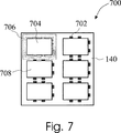
Die vorliegende Erfindung soll nicht darauf beschränkt werden. Der erfinderische Grundgedanke lässt sich auch mit einer balkenförmigen, mehreren balkenförmigen oder anderen Kontaktanordnungen realisieren. Zum Beispiel reicht für die Kontaktanordnung
Existieren mehrere Teile der Kontaktiereinheit, ist es wie bereits in bezug auf
Daher ist das erste Testobjekt in 12 Bereiche I bis XII unterteilt. Jeder dieser Bereiche hat dieselbe Größe wie der Test-Bereich
Um bei der Beschreibung der Testmethode, auf entsprechende Verschiebungen verweisen zu könne, sind in
In
Der Test-Bereich
Das Testverfahren beruht auch in diesem Beispiel auf das in bezug auf
Danach wird die Kontaktiereinheit und das Substrat relativ zueinander verschoben (siehe
Die bisherigen Ausführungsbeispiele haben beispielhaft auf ein Testverfahren mit einem Strahl geladener Teilchen Bezug genommen. Da diese Testverfahren sehr empfindlich sind, ist es bevorzugt, die Testvorrichtung, d. h. die Strahlquelle, die Strahlformung, die Strahlablenkung und die Signaldetektion, nicht zu verschieben. Dadurch kann zum Beispiel eine Dejustage auf Grund von Vibrationen verringert werden.The previous embodiments have, for example, referred to a test procedure with a charged particle beam. Since these test methods are very sensitive, it is preferable to use the test device, i. H. the beam source, the beam shaping, the beam deflection and the signal detection, not to move. As a result, for example, a maladjustment due to vibrations can be reduced.
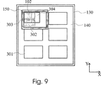
In
Da bei dem in bezug auf
In
Zusätzlich zu der Positionierung der Messvorrichtung mit dem Test-Bereich
Der Test des zweiten Bereichs
Nach dem Testen des zweiten Bereichs
Nach der Verschiebung
Durch weitere Verschiebungen der Kontaktiereinheit und der optischen Achse der Testvorrichtung relativ zum Halter
Gemäß den im Bezug auf die vorliegende Erfindung beschriebenen Ausführungsformen kann eine große Flexibilität gewährleistet werden, die einen Wechsel von Kontaktiereinheiten unnötig macht. Zudem können die immer größer werdenden Displays mit Hilfe von einfach ausgeführte Kontaktanordnungen kontaktiert werden, da die Kontaktiereinheit einer Verschiebung der Testobjekte und der optischen Achse des Korpuskularstrahl-Testgerätes relativ zueinander folgen kann.According to the embodiments described in relation to the present invention, a great flexibility can be ensured which makes a change of contacting units unnecessary. In addition, the increasingly large displays can be contacted by means of simple contact arrangements, since the contacting unit can follow a displacement of the test objects and the optical axis of the particle beam test apparatus relative to each other.
Claims (31)
Priority Applications (11)
| Application Number | Priority Date | Filing Date | Title |
|---|---|---|---|
| DE10253717A DE10253717B4 (en) | 2002-11-18 | 2002-11-18 | Device for contacting for the test of at least one test object, test system and method for testing test objects |
| EP03026267A EP1420259A1 (en) | 2002-11-18 | 2003-11-14 | Apparatus and method for contacting of test objects |
| AU2003292020A AU2003292020A1 (en) | 2002-11-18 | 2003-11-14 | Device and methods for contacting objects to be tested |
| CN200910150538XA CN101625823B (en) | 2002-11-18 | 2003-11-14 | Apparatus and method for contacting test objects |
| PCT/EP2003/012739 WO2004046740A1 (en) | 2002-11-18 | 2003-11-14 | Device and methods for contacting objects to be tested |
| CNB2003801035614A CN100526897C (en) | 2002-11-18 | 2003-11-14 | Device and methods for contacting objects to be tested |
| TW092131977A TWI267644B (en) | 2002-11-18 | 2003-11-14 | Apparatus and method for contacting of test objects |
| KR1020057008488A KR100817597B1 (en) | 2002-11-18 | 2003-11-14 | Device and methods for contacting objects to be tested |
| JP2004552594A JP2006506629A (en) | 2002-11-18 | 2003-11-14 | Apparatus and method for contact of a specimen |
| US10/716,102 US7135875B2 (en) | 2002-11-18 | 2003-11-18 | Apparatus and method for contacting of test objects |
| US11/398,052 US7474108B2 (en) | 2002-11-18 | 2006-04-05 | Apparatus and method for contacting of test objects |
Applications Claiming Priority (1)
| Application Number | Priority Date | Filing Date | Title |
|---|---|---|---|
| DE10253717A DE10253717B4 (en) | 2002-11-18 | 2002-11-18 | Device for contacting for the test of at least one test object, test system and method for testing test objects |
Publications (2)
| Publication Number | Publication Date |
|---|---|
| DE10253717A1 DE10253717A1 (en) | 2004-05-27 |
| DE10253717B4 true DE10253717B4 (en) | 2011-05-19 |
Family
ID=32115567
Family Applications (1)
| Application Number | Title | Priority Date | Filing Date |
|---|---|---|---|
| DE10253717A Expired - Fee Related DE10253717B4 (en) | 2002-11-18 | 2002-11-18 | Device for contacting for the test of at least one test object, test system and method for testing test objects |
Country Status (9)
| Country | Link |
|---|---|
| US (2) | US7135875B2 (en) |
| EP (1) | EP1420259A1 (en) |
| JP (1) | JP2006506629A (en) |
| KR (1) | KR100817597B1 (en) |
| CN (2) | CN101625823B (en) |
| AU (1) | AU2003292020A1 (en) |
| DE (1) | DE10253717B4 (en) |
| TW (1) | TWI267644B (en) |
| WO (1) | WO2004046740A1 (en) |
Families Citing this family (22)
| Publication number | Priority date | Publication date | Assignee | Title |
|---|---|---|---|---|
| DE10253717B4 (en) | 2002-11-18 | 2011-05-19 | Applied Materials Gmbh | Device for contacting for the test of at least one test object, test system and method for testing test objects |
| US7319335B2 (en) * | 2004-02-12 | 2008-01-15 | Applied Materials, Inc. | Configurable prober for TFT LCD array testing |
| US7355418B2 (en) * | 2004-02-12 | 2008-04-08 | Applied Materials, Inc. | Configurable prober for TFT LCD array test |
| US6833717B1 (en) * | 2004-02-12 | 2004-12-21 | Applied Materials, Inc. | Electron beam test system with integrated substrate transfer module |
| US8083853B2 (en) | 2004-05-12 | 2011-12-27 | Applied Materials, Inc. | Plasma uniformity control by gas diffuser hole design |
| US8328939B2 (en) * | 2004-05-12 | 2012-12-11 | Applied Materials, Inc. | Diffuser plate with slit valve compensation |
| US8074599B2 (en) | 2004-05-12 | 2011-12-13 | Applied Materials, Inc. | Plasma uniformity control by gas diffuser curvature |
| US7429410B2 (en) * | 2004-09-20 | 2008-09-30 | Applied Materials, Inc. | Diffuser gravity support |
| KR100780759B1 (en) * | 2005-01-24 | 2007-11-30 | 삼성전자주식회사 | TFT Array Inspecting Apparatus |
| US7535238B2 (en) * | 2005-04-29 | 2009-05-19 | Applied Materials, Inc. | In-line electron beam test system |
| KR100643389B1 (en) * | 2005-07-04 | 2006-11-10 | 삼성전자주식회사 | Apparatus for inspecting tft substrate and method of inspecting tft substrate |
| CN101400991B (en) * | 2006-03-14 | 2013-03-20 | 应用材料公司 | Method to reduce cross talk in a multi column e-beam test system |
| US7786742B2 (en) * | 2006-05-31 | 2010-08-31 | Applied Materials, Inc. | Prober for electronic device testing on large area substrates |
| KR101023890B1 (en) * | 2006-05-31 | 2011-03-22 | 어플라이드 머티어리얼스, 인코포레이티드 | Mini-prober for tft-lcd testing |
| US7602199B2 (en) * | 2006-05-31 | 2009-10-13 | Applied Materials, Inc. | Mini-prober for TFT-LCD testing |
| US20080317973A1 (en) * | 2007-06-22 | 2008-12-25 | White John M | Diffuser support |
| EP2164310A4 (en) * | 2007-07-04 | 2011-01-05 | Sharp Kk | Display module, liquid crystal display device and method for manufacturing display module |
| TWI426286B (en) * | 2010-08-02 | 2014-02-11 | Ind Tech Res Inst | Measurement apparatuses for conductive patterns on substrates |
| JP6300553B2 (en) * | 2014-02-12 | 2018-03-28 | 株式会社日立ハイテクサイエンス | Charged particle beam equipment |
| TWI676033B (en) * | 2018-11-09 | 2019-11-01 | 京元電子股份有限公司 | Semiconductor testing carrier with buffering container and testing apparatus thereof |
| CN111190087B (en) * | 2018-11-15 | 2022-03-15 | 京元电子股份有限公司 | Semiconductor element test carrying disc with floating containing seat and test equipment thereof |
| CN109765479B (en) * | 2019-01-28 | 2021-10-01 | 合肥京东方视讯科技有限公司 | Device and method for detecting missing parts of circuit board |
Citations (6)
| Publication number | Priority date | Publication date | Assignee | Title |
|---|---|---|---|---|
| US4532423A (en) * | 1982-05-31 | 1985-07-30 | Tokyo Shibaura Denki Kabushiki Kaisha | IC Tester using an electron beam capable of easily setting a probe card unit for wafers & packaged IC's to be tested |
| DE3636316A1 (en) * | 1985-10-25 | 1987-04-30 | Hitachi Ltd | DEVICE FOR SCANING SURFACES USING A CHARGED PARTICLE RAY |
| EP0402499A1 (en) * | 1989-06-13 | 1990-12-19 | Siemens Aktiengesellschaft | Process for testing a circuit board with a particle beam |
| EP0523594A1 (en) * | 1991-07-15 | 1993-01-20 | ICT Integrated Circuit Testing Gesellschaft für HalbleiterprÀ¼ftechnik mbH | Method for testing substrater for liquid crystal displays (LCD) using a corpuscular beam |
| US5691764A (en) * | 1994-08-05 | 1997-11-25 | Tokyo Electron Limited | Apparatus for examining target objects such as LCD panels |
| US5982190A (en) * | 1998-02-04 | 1999-11-09 | Toro-Lira; Guillermo L. | Method to determine pixel condition on flat panel displays using an electron beam |
Family Cites Families (38)
| Publication number | Priority date | Publication date | Assignee | Title |
|---|---|---|---|---|
| US4471298A (en) | 1981-12-11 | 1984-09-11 | Cirdyne, Inc. | Apparatus for automatically electrically testing printed circuit boards |
| JPS5976439A (en) * | 1982-10-22 | 1984-05-01 | Fujitsu Ltd | Diagnostic method of semiconductor device |
| JPS622552A (en) | 1985-06-27 | 1987-01-08 | Matsushita Electric Ind Co Ltd | Inspecting unit for semiconductor and inspecting method for semiconductor |
| US4965515A (en) | 1986-10-15 | 1990-10-23 | Tokyo Electron Limited | Apparatus and method of testing a semiconductor wafer |
| US4772846A (en) * | 1986-12-29 | 1988-09-20 | Hughes Aircraft Company | Wafer alignment and positioning apparatus for chip testing by voltage contrast electron microscopy |
| JPH0817196B2 (en) * | 1988-03-22 | 1996-02-21 | 東京エレクトロン株式会社 | Electron beam probe device |
| US6288561B1 (en) | 1988-05-16 | 2001-09-11 | Elm Technology Corporation | Method and apparatus for probing, testing, burn-in, repairing and programming of integrated circuits in a closed environment using a single apparatus |
| JP2694345B2 (en) | 1988-07-14 | 1997-12-24 | 東京エレクトロン株式会社 | Inspection device |
| JP2678178B2 (en) * | 1988-11-18 | 1997-11-17 | 東京エレクトロン株式会社 | Probing method and probe device |
| US4985676A (en) | 1989-02-17 | 1991-01-15 | Tokyo Electron Limited | Method and apparatus of performing probing test for electrically and sequentially testing semiconductor device patterns |
| US4965676A (en) * | 1989-02-28 | 1990-10-23 | Ricoh Corporation And Ricoh Company, Ltd. | Facsimile remote diagnostic system |
| JPH06110069A (en) * | 1992-09-29 | 1994-04-22 | Matsushita Electric Ind Co Ltd | Method and device for repairing defect of electronic component |
| JPH06151532A (en) | 1992-11-13 | 1994-05-31 | Tokyo Electron Yamanashi Kk | Prober |
| JP2765427B2 (en) * | 1993-04-13 | 1998-06-18 | 日本電気株式会社 | Method and apparatus for inspecting interconnections inside semiconductor integrated circuit |
| DE69326003T2 (en) | 1993-09-20 | 1999-11-25 | Hewlett Packard Gmbh | Test apparatus for testing and handling a variety of devices |
| US5644245A (en) | 1993-11-24 | 1997-07-01 | Tokyo Electron Limited | Probe apparatus for inspecting electrical characteristics of a microelectronic element |
| US5528158A (en) | 1994-04-11 | 1996-06-18 | Xandex, Inc. | Probe card changer system and method |
| WO1996029607A1 (en) | 1995-03-18 | 1996-09-26 | Tokyo Electron Limited | Method and apparatus for inspecting substrate |
| JPH08115954A (en) * | 1994-10-14 | 1996-05-07 | Tokyo Electron Ltd | Inspection equipment |
| US5621333A (en) | 1995-05-19 | 1997-04-15 | Microconnect, Inc. | Contact device for making connection to an electronic circuit device |
| TW301099B (en) | 1995-07-14 | 1997-03-21 | Tokyo Electron Co Ltd | |
| US6046599A (en) | 1996-05-20 | 2000-04-04 | Microconnect, Inc. | Method and device for making connection |
| US5923180A (en) | 1997-02-04 | 1999-07-13 | Hewlett-Packard Company | Compliant wafer prober docking adapter |
| US6268661B1 (en) * | 1999-08-31 | 2001-07-31 | Nec Corporation | Semiconductor device and method of its fabrication |
| JP3423979B2 (en) | 1997-07-11 | 2003-07-07 | 東京エレクトロン株式会社 | Probe method and probe device |
| US5962190A (en) * | 1997-08-27 | 1999-10-05 | E. I. Du Pont De Nemours And Company | Photopolymerizable compositions having improved sidewall geometry and development latitude |
| US6075245A (en) * | 1998-01-12 | 2000-06-13 | Toro-Lira; Guillermo L. | High speed electron beam based system for testing large area flat panel displays |
| US6246245B1 (en) | 1998-02-23 | 2001-06-12 | Micron Technology, Inc. | Probe card, test method and test system for semiconductor wafers |
| JP3538696B2 (en) * | 1998-08-20 | 2004-06-14 | ジェネシス・テクノロジー株式会社 | Method of assembling probe device |
| US6198299B1 (en) | 1998-08-27 | 2001-03-06 | The Micromanipulator Company, Inc. | High Resolution analytical probe station |
| US6343369B1 (en) | 1998-09-15 | 2002-01-29 | Microconnect, Inc. | Methods for making contact device for making connection to an electronic circuit device and methods of using the same |
| JP2000311930A (en) | 1999-04-28 | 2000-11-07 | Agilent Technologies Japan Ltd | Semiconductor inspection apparatus and method for specifying attribute of each die on wafer in the apparatus |
| JP2001024038A (en) * | 1999-07-05 | 2001-01-26 | Hitachi Ltd | Probe positioning method and apparatus and method of evaluating member using the same |
| JP4015352B2 (en) * | 2000-02-22 | 2007-11-28 | 株式会社日立製作所 | Inspection method using charged particle beam |
| JP2001318116A (en) * | 2000-05-11 | 2001-11-16 | Micronics Japan Co Ltd | Inspection apparatus for display panel board |
| US20020135395A1 (en) * | 2001-02-08 | 2002-09-26 | Pete Smith | System and method for testing a display device |
| JP3468755B2 (en) | 2001-03-05 | 2003-11-17 | 石川島播磨重工業株式会社 | LCD drive board inspection equipment |
| DE10253717B4 (en) | 2002-11-18 | 2011-05-19 | Applied Materials Gmbh | Device for contacting for the test of at least one test object, test system and method for testing test objects |
-
2002
- 2002-11-18 DE DE10253717A patent/DE10253717B4/en not_active Expired - Fee Related
-
2003
- 2003-11-14 KR KR1020057008488A patent/KR100817597B1/en active IP Right Grant
- 2003-11-14 CN CN200910150538XA patent/CN101625823B/en not_active Expired - Lifetime
- 2003-11-14 TW TW092131977A patent/TWI267644B/en not_active IP Right Cessation
- 2003-11-14 JP JP2004552594A patent/JP2006506629A/en active Pending
- 2003-11-14 AU AU2003292020A patent/AU2003292020A1/en not_active Abandoned
- 2003-11-14 EP EP03026267A patent/EP1420259A1/en not_active Withdrawn
- 2003-11-14 CN CNB2003801035614A patent/CN100526897C/en not_active Expired - Lifetime
- 2003-11-14 WO PCT/EP2003/012739 patent/WO2004046740A1/en active Application Filing
- 2003-11-18 US US10/716,102 patent/US7135875B2/en not_active Expired - Lifetime
-
2006
- 2006-04-05 US US11/398,052 patent/US7474108B2/en not_active Expired - Fee Related
Patent Citations (6)
| Publication number | Priority date | Publication date | Assignee | Title |
|---|---|---|---|---|
| US4532423A (en) * | 1982-05-31 | 1985-07-30 | Tokyo Shibaura Denki Kabushiki Kaisha | IC Tester using an electron beam capable of easily setting a probe card unit for wafers & packaged IC's to be tested |
| DE3636316A1 (en) * | 1985-10-25 | 1987-04-30 | Hitachi Ltd | DEVICE FOR SCANING SURFACES USING A CHARGED PARTICLE RAY |
| EP0402499A1 (en) * | 1989-06-13 | 1990-12-19 | Siemens Aktiengesellschaft | Process for testing a circuit board with a particle beam |
| EP0523594A1 (en) * | 1991-07-15 | 1993-01-20 | ICT Integrated Circuit Testing Gesellschaft für HalbleiterprÀ¼ftechnik mbH | Method for testing substrater for liquid crystal displays (LCD) using a corpuscular beam |
| US5691764A (en) * | 1994-08-05 | 1997-11-25 | Tokyo Electron Limited | Apparatus for examining target objects such as LCD panels |
| US5982190A (en) * | 1998-02-04 | 1999-11-09 | Toro-Lira; Guillermo L. | Method to determine pixel condition on flat panel displays using an electron beam |
Also Published As
| Publication number | Publication date |
|---|---|
| DE10253717A1 (en) | 2004-05-27 |
| JP2006506629A (en) | 2006-02-23 |
| KR100817597B1 (en) | 2008-03-31 |
| CN101625823A (en) | 2010-01-13 |
| CN100526897C (en) | 2009-08-12 |
| TW200417737A (en) | 2004-09-16 |
| CN101625823B (en) | 2013-04-17 |
| US7474108B2 (en) | 2009-01-06 |
| TWI267644B (en) | 2006-12-01 |
| EP1420259A1 (en) | 2004-05-19 |
| WO2004046740A1 (en) | 2004-06-03 |
| US20040145383A1 (en) | 2004-07-29 |
| CN1714298A (en) | 2005-12-28 |
| KR20050075395A (en) | 2005-07-20 |
| AU2003292020A1 (en) | 2004-06-15 |
| US20060181290A1 (en) | 2006-08-17 |
| US7135875B2 (en) | 2006-11-14 |
Similar Documents
| Publication | Publication Date | Title |
|---|---|---|
| DE10253717B4 (en) | Device for contacting for the test of at least one test object, test system and method for testing test objects | |
| DE102004058483B4 (en) | Device for testing products for faults, sensor positioning methods and sensor movement methods | |
| DE19822724C2 (en) | Pattern error control system and pattern error control method | |
| DE10000365B4 (en) | Stress contrast method for detecting defects in a patterned substrate | |
| DE102004061533A1 (en) | Method and device for probe navigation and defect testing device | |
| DE102014204876A1 (en) | Inspection procedure and inspection device | |
| DE112016004904T5 (en) | Verification method and verification device | |
| DE10214191A1 (en) | Microscope system for medical application, controls image formation unit to form magnified image of specimen, based on electronic zoom magnification factor and magnifying power of optical systems inserted at optical path | |
| DE112010002934T5 (en) | Microscope with a beam of charged particles and measuring method therefor | |
| DE102009019426B4 (en) | A method of inspecting the settling time of a deflection amplifier and method of assessing the failure of a deflection amplifier | |
| DE102007015232A1 (en) | A charged particle beam device, an abnormality detection method for a DA converter unit, a charged particle beam writing method, and a mask | |
| EP1116932A2 (en) | Measuring apparatus and method for measuring structures on a substrat | |
| DE19802848B4 (en) | Method and apparatus for testing a substrate | |
| DE112012002533T5 (en) | Table assembly and control method for a table assembly | |
| DE112014004151T5 (en) | A method for correcting the inclination of a charged particle beam and a charged particle beam device | |
| DE102006015714B4 (en) | Light-assisted testing of an opto-electronic module | |
| DE19721313A1 (en) | Test specimen critical dimension measurement system for e.g. semiconductor manufacture | |
| DE10238579A1 (en) | Image-based inspection system for printed circuit boards, has controller to control operation of position-altering unit using representation of object that is generated by mapping unit | |
| WO2011127962A1 (en) | Method and device for contacting a row of contact surfaces with probe tips | |
| DE102007025304A1 (en) | Method for improving the reproducibility of a coordinate measuring machine and its accuracy | |
| DE102007039982B3 (en) | Method for optical inspection and visualization of the optical knife values obtained from disc-shaped objects | |
| DD219567A5 (en) | METHOD AND DEVICE FOR ERROR-CONTROLLING TRANSMISSION MASKS OF LINEAR PATTERNS OF INTEGRATED CIRCUITS | |
| EP0991934A1 (en) | Method for focusing during imaging of structured surfaces of disc-shaped objects | |
| EP1521973B1 (en) | Control device of an optoelectronic device having improved testing properties | |
| DE102019212936A1 (en) | IMAGE TEST DEVICE |
Legal Events
| Date | Code | Title | Description |
|---|---|---|---|
| OP8 | Request for examination as to paragraph 44 patent law | ||
| R020 | Patent grant now final |
Effective date: 20110820 |
|
| R119 | Application deemed withdrawn, or ip right lapsed, due to non-payment of renewal fee |