DE102004052634B4 - Method for producing heat flow measuring elements - Google Patents
Method for producing heat flow measuring elements Download PDFInfo
- Publication number
- DE102004052634B4 DE102004052634B4 DE102004052634A DE102004052634A DE102004052634B4 DE 102004052634 B4 DE102004052634 B4 DE 102004052634B4 DE 102004052634 A DE102004052634 A DE 102004052634A DE 102004052634 A DE102004052634 A DE 102004052634A DE 102004052634 B4 DE102004052634 B4 DE 102004052634B4
- Authority
- DE
- Germany
- Prior art keywords
- dummy pattern
- heat
- film
- substrate
- flow sensor
- Prior art date
- Legal status (The legal status is an assumption and is not a legal conclusion. Google has not performed a legal analysis and makes no representation as to the accuracy of the status listed.)
- Expired - Fee Related
Links
- 238000004519 manufacturing process Methods 0.000 title claims abstract description 29
- 239000000758 substrate Substances 0.000 claims abstract description 53
- 230000001681 protective effect Effects 0.000 claims abstract description 29
- 230000007547 defect Effects 0.000 claims abstract description 17
- 239000012528 membrane Substances 0.000 claims abstract description 8
- 238000012545 processing Methods 0.000 claims abstract description 8
- 238000000034 method Methods 0.000 claims description 29
- XLYOFNOQVPJJNP-UHFFFAOYSA-N water Substances O XLYOFNOQVPJJNP-UHFFFAOYSA-N 0.000 claims description 13
- 230000020169 heat generation Effects 0.000 claims description 12
- 230000004907 flux Effects 0.000 claims description 10
- 230000015572 biosynthetic process Effects 0.000 claims description 3
- 238000012360 testing method Methods 0.000 claims description 2
- 238000011835 investigation Methods 0.000 abstract description 4
- 239000010408 film Substances 0.000 description 76
- 239000010409 thin film Substances 0.000 description 16
- BASFCYQUMIYNBI-UHFFFAOYSA-N platinum Chemical compound [Pt] BASFCYQUMIYNBI-UHFFFAOYSA-N 0.000 description 12
- 229910052697 platinum Inorganic materials 0.000 description 7
- 238000004544 sputter deposition Methods 0.000 description 7
- 229910052581 Si3N4 Inorganic materials 0.000 description 6
- HEMHJVSKTPXQMS-UHFFFAOYSA-M Sodium hydroxide Chemical compound [OH-].[Na+] HEMHJVSKTPXQMS-UHFFFAOYSA-M 0.000 description 6
- 238000000206 photolithography Methods 0.000 description 6
- HQVNEWCFYHHQES-UHFFFAOYSA-N silicon nitride Chemical compound N12[Si]34N5[Si]62N3[Si]51N64 HQVNEWCFYHHQES-UHFFFAOYSA-N 0.000 description 6
- 239000004020 conductor Substances 0.000 description 5
- 238000005868 electrolysis reaction Methods 0.000 description 5
- 238000005530 etching Methods 0.000 description 5
- 238000007689 inspection Methods 0.000 description 5
- 238000001312 dry etching Methods 0.000 description 4
- 239000000463 material Substances 0.000 description 4
- 238000002360 preparation method Methods 0.000 description 4
- WGTYBPLFGIVFAS-UHFFFAOYSA-M tetramethylammonium hydroxide Chemical compound [OH-].C[N+](C)(C)C WGTYBPLFGIVFAS-UHFFFAOYSA-M 0.000 description 4
- 238000001039 wet etching Methods 0.000 description 4
- 230000006866 deterioration Effects 0.000 description 3
- 230000000694 effects Effects 0.000 description 3
- 238000005259 measurement Methods 0.000 description 3
- 229910052710 silicon Inorganic materials 0.000 description 3
- 239000010703 silicon Substances 0.000 description 3
- 238000007740 vapor deposition Methods 0.000 description 3
- 239000013078 crystal Substances 0.000 description 2
- 239000012530 fluid Substances 0.000 description 2
- 238000000059 patterning Methods 0.000 description 2
- 150000003057 platinum Chemical class 0.000 description 2
- 230000000087 stabilizing effect Effects 0.000 description 2
- 229940073455 tetraethylammonium hydroxide Drugs 0.000 description 2
- LRGJRHZIDJQFCL-UHFFFAOYSA-M tetraethylazanium;hydroxide Chemical compound [OH-].CC[N+](CC)(CC)CC LRGJRHZIDJQFCL-UHFFFAOYSA-M 0.000 description 2
- 238000013459 approach Methods 0.000 description 1
- 238000002485 combustion reaction Methods 0.000 description 1
- 238000007796 conventional method Methods 0.000 description 1
- 230000007797 corrosion Effects 0.000 description 1
- 238000005260 corrosion Methods 0.000 description 1
- 230000001419 dependent effect Effects 0.000 description 1
- 238000000151 deposition Methods 0.000 description 1
- 238000001035 drying Methods 0.000 description 1
- 238000003754 machining Methods 0.000 description 1
- 239000011159 matrix material Substances 0.000 description 1
- 238000012552 review Methods 0.000 description 1
- 230000035945 sensitivity Effects 0.000 description 1
- 238000010998 test method Methods 0.000 description 1
Images


Classifications
-
- G—PHYSICS
- G01—MEASURING; TESTING
- G01F—MEASURING VOLUME, VOLUME FLOW, MASS FLOW OR LIQUID LEVEL; METERING BY VOLUME
- G01F1/00—Measuring the volume flow or mass flow of fluid or fluent solid material wherein the fluid passes through a meter in a continuous flow
- G01F1/68—Measuring the volume flow or mass flow of fluid or fluent solid material wherein the fluid passes through a meter in a continuous flow by using thermal effects
-
- H—ELECTRICITY
- H01—ELECTRIC ELEMENTS
- H01L—SEMICONDUCTOR DEVICES NOT COVERED BY CLASS H10
- H01L27/00—Devices consisting of a plurality of semiconductor or other solid-state components formed in or on a common substrate
- H01L27/14—Devices consisting of a plurality of semiconductor or other solid-state components formed in or on a common substrate including semiconductor components sensitive to infrared radiation, light, electromagnetic radiation of shorter wavelength or corpuscular radiation and specially adapted either for the conversion of the energy of such radiation into electrical energy or for the control of electrical energy by such radiation
- H01L27/144—Devices controlled by radiation
- H01L27/146—Imager structures
- H01L27/14683—Processes or apparatus peculiar to the manufacture or treatment of these devices or parts thereof
- H01L27/14687—Wafer level processing
-
- H—ELECTRICITY
- H01—ELECTRIC ELEMENTS
- H01L—SEMICONDUCTOR DEVICES NOT COVERED BY CLASS H10
- H01L27/00—Devices consisting of a plurality of semiconductor or other solid-state components formed in or on a common substrate
- H01L27/14—Devices consisting of a plurality of semiconductor or other solid-state components formed in or on a common substrate including semiconductor components sensitive to infrared radiation, light, electromagnetic radiation of shorter wavelength or corpuscular radiation and specially adapted either for the conversion of the energy of such radiation into electrical energy or for the control of electrical energy by such radiation
- H01L27/144—Devices controlled by radiation
- H01L27/146—Imager structures
- H01L27/14643—Photodiode arrays; MOS imagers
Abstract
Verfahren zur Herstellung von Wärme-Flussmesselementen (12), die jeweils einen isolierenden Halterunorgesehen ist, sowie eine Membran (11), die durch teilweises Entfernen des Substrats (1) ausgebildet wird, mit folgenden Schritten: (a) Erzeugung mehrerer Flusssensormuster (23) auf dem Halterungsfilm (2), welche aus einem Wärmewiderstandsfilm bestehen, und jeweils einen Wärmeerzeugungswiderstand (4) und einen Temperaturmesswiderstand (5) aufweisen; (b) Erzeugen eines Attrappenmusters (7) auf dem Halterungsfilm (2), das aus dem Wärmewiderstandsfilm ausgebildet wird, und welches elektrische Verbindungen der mehreren Flusssensormuster (23) zur Verfügung stellt; (b1) Ausbilden eines Schutzfilms (3) auf den Flusssensormustern (23) und dem Attrappenmuster (7); (c) Durchführung einer Bearbeitung zum Erzeugen von Wärme durch Anlegen von Spannung an die Wärmeerzeugungswiderstände (4) unter Verwendung des Attrappenmusters (7), bis keine Schwankungen der Widerstandswerte der Wärmeerzeugungswiderstände (4) mehr auftreten, und Durchführung einer Untersuchung in Bezug auf Fehlstellen des Schutzfilms durch Anlegen von Spannung zwischen den...A method for producing heat flow measuring elements (12), each of which does not have an insulating holder, and a membrane (11) which is formed by partially removing the substrate (1), with the following steps: (a) Generation of a plurality of flow sensor patterns (23) on the holding film (2) which are composed of a heat resistance film and each have a heat generating resistor (4) and a temperature measuring resistor (5); (b) forming a dummy pattern (7) on the holding film (2), which is formed from the heat resistance film and which provides electrical connections of the plurality of flow sensor patterns (23); (b1) forming a protective film (3) on the flow sensor patterns (23) and the dummy pattern (7); (c) Carrying out a processing for generating heat by applying voltage to the heat generating resistors (4) using the dummy pattern (7) until there are no more fluctuations in the resistance values of the heat generating resistors (4), and carrying out an investigation with regard to defects in the Protective film by applying voltage between the ...
Description
Die vorliegende Erfindung betrifft Flussmesselemente für einen Flusssensor, der das Volumen der Ansaugluft und dergleichen bei einer Brennkraftmaschine misst, und speziell Wärme-Flussmesselemente, die jeweils einen Membranaufbau aufweisen, bei welchem ein Dünnfilmsensorabschnitt auf einem Substrat vorgesehen ist, und betrifft weiterhin ein Verfahren zur Herstellung eines derartigen Flussmesselements.The present invention relates to flow measuring elements for a flow sensor that measures the volume of intake air and the like in an internal combustion engine, and more particularly to heat flow sensing elements each having a diaphragm structure in which a thin film sensor section is provided on a substrate, and further relates to a method of manufacturing such a flow meter.
Bei herkömmlichen Verfahren zur Herstellung von Wärme-Flussmesselementen, die jeweils einen Membranaufbau aufweisen, werden nach Ausbildung von Dünnfilmsensorabschnitten auf einem Wärmewiderstandsfilm auf einer Substratoberfläche Bereiche des Substrats unterhalb der Dünnfilmsensorabschnitte zur Ausbildung von Membranen entfernt. Das Substrat wird dann geschnitten und so auf einzelne Flussmesselemente aufgeteilt. Diese getrennten Flussmesselemente werden nach Bearbeitung in einen Flusssensor eingebaut.In conventional methods of manufacturing heat flux sensing elements each having a diaphragm structure, after forming thin film sensor portions on a thermal resistance film on a substrate surface, portions of the substrate beneath the thin film sensor portions are removed to form diaphragms. The substrate is then cut and split into individual flow measuring elements. These separate flow measuring elements are installed in a flow sensor after machining.
Die japanische offengelegte Patentanmeldung
Der Dünnfilmsensorabschnitt jedes dieser Flussmesselemente weist einen Wärmeerzeugungswiderstand auf, dessen Widerstandswert sich in Abhängigkeit von der erheblichen Wärme ändert, die durch Stromversorgung hervorgerufen wird; die Eigenschaften des Wärmeerzeugungswiderstands können sich daher gegenüber dem Ursprungszustand ändern. Daher wird es erforderlich, die Eigenschaften dadurch zu stabilisieren, dass eine elektrische Verbindung zwischen den Flussmesselementen und dem Äußeren bereitgestellt wird, und die Flussmesselemente so mit Strom versorgt werden, dass vorher ihre jeweiligen Wärmeerzeugungswiderstände auf eine vorbestimmte Temperatur oder mehr gebracht werden.The thin-film sensor portion of each of these flow sensing elements has a heat-generating resistor whose resistance value changes depending on the significant heat caused by the power supply; the properties of the heat generation resistor may therefore change from the original state. Therefore, it becomes necessary to stabilize the characteristics by providing an electrical connection between the flow sensing elements and the exterior, and to energize the flow sensing elements to advance their respective heat generating resistances to a predetermined temperature or more.
Ein Beispiel für die Vorgehensweisen zur Bereitstellung elektrischer Verbindungen wie voranstehend geschildert, besteht darin, die Elektroden der Flussmesselemente in direkten Kontakt mit Stiften zu versetzen. Allerdings tritt hierbei das Problem auf, dass die Elektroden beschädigt werden können, was zu einer verringerten Verlässlichkeit führt.An example of the procedures for providing electrical connections as described above is to put the electrodes of the flow sensing elements in direct contact with pins. However, there is a problem that the electrodes may be damaged, resulting in reduced reliability.
Um eine derartige, verringerte Verlässlichkeit zu verhindern, gibt es die Vorgehensweise, den Strom nach Zusammenbau eines Flusssensors in einem Zustand zuzuführen, in welchem leicht eine Verbindung mit dem Äußeren erreicht werden kann. Eine Vergrößerung der Abmessungen der Anordnung führt jedoch zu einer Vergrößerung der Abmessungen der Einrichtungen für die Stromversorgung, was die Handhabbarkeit beeinträchtigt.In order to prevent such a reduced reliability, there is a way to supply the current after assembly of a flow sensor in a state in which a connection with the outside can be easily achieved. However, an increase in the size of the arrangement leads to an increase in the dimensions of the devices for the power supply, which impairs the handling.
Bei der Bearbeitung der voranstehend geschilderten Flussmesselemente wird darüber hinaus ein Schutzfilm auf den Dünnfilmsensorabschnitten eines Wärmewiderstandsfilms hergestellt. Falls dieser Schutzfilm Defekte in Bezug auf die Abdeckung infolge von Spalten oder Rissen, Fremdkörpern und dergleichen aufweist, kann Elektrolyse an diesen Fehlstellen der Abdeckung auftreten, wenn die Flussmesselemente Wasser ausgesetzt werden. Da Änderungen der Widerstandswerte zu Änderungen der Eigenschaften gegenüber dem Ursprungszustand führen, können im schlimmsten Fall die Widerstände offen liegen. Es wird daher erforderlich, zu überprüfen, ob sich Fehlstellen infolge von Spalten oder Rissen, Fremdkörpern oder dergleichen bis zum Wärmewiderstandsfilm erstrecken oder nicht, jedoch ist es schwierig, die Flussmesselemente in Abschnitten zu betrachten. In Bezug auf Fehlstellen infolge von Fremdkörpern wird die Herstellung so gesteuert, dass die Flussmesselemente direkt von der Oberflächenseite aus mit dem Auge oder durch ein Mikroskop betrachtet werden, usw., in Bezug auf die Größe von Fremdkörpern, und wird dann, wenn die Gröle einen vorbestimmten Wert überschreitet, der Fremdkörper als Fehlstelle angesehen. Abhängig von der Form eines Fremdkörpers kann selbst dann, wenn der Fremdkörper bei direkter Beobachtung von der Oberfläche aus klein aussieht, es sich tatsächlich um eine große Fehlstelle handeln. Daher ist es schwierig, exakt sämtliche Fehlstellen infolge von Fremdkörpern mit Hilfe einer direkten Betrachtung von der Oberflächenseite mit dem Auge oder mit einem Mikroskop usw. zu erfassen. Entsprechendes gilt für Fehlstellen infolge von Rissen oder Spalten. Eine Untersuchung durch direkte Beobachtung von der Oberfläche aus bringt daher das Problem einer möglichen Beeinträchtigung der Verlässlichkeit mit sich.In the processing of the above-described flow measuring elements, moreover, a protective film is formed on the thin film sensor portions of a thermal resistance film. If this protective film has defects in coverage due to crevices or cracks, foreign matters and the like, electrolysis may occur at these defects of the cover when the flow sensing elements are exposed to water. Since changes in the resistance values lead to changes in the properties relative to the original state, in the worst case the resistances can be open. It therefore becomes necessary to check whether or not voids due to crevices or cracks, foreign matter or the like extend to the heat-resistant film or not, but it is difficult to view the flow-measuring elements in sections. With respect to defects due to foreign matter, the production is controlled so that the flow measurement elements are viewed directly from the surface side by eye or microscope, etc., in terms of the size of foreign matter, and then when the size becomes one exceeds predetermined value, the foreign body regarded as a defect. Depending on the shape of a foreign body, even if the foreign matter looks small when viewed directly from the surface, it may actually be a large defect. Therefore, it is difficult to accurately detect all defects due to foreign matter by direct observation from the surface side with the eye or a microscope, and so on. The same applies to defects due to cracks or crevices. Examination by direct observation from the surface therefore poses the problem of possible deterioration of reliability.
Um eine derartige Beeinträchtigkeit der Verlässlichkeit zu verhindern, gibt es die Vorgehensweise, eine Untersuchung anstelle mittels Durchführung direkter Beobachtungen dadurch durchzuführen, dass die Flussmesselemente mit ihren Körpern in Wasser eingetaucht werden, und mit dem Auge oder mit einem Mikroskop und dergleichen die Erzeugung von Luftblasen infolge von Elektrolyse an Fehlstellen der Abdeckung beobachtet wird. Allerdings ist in diesem Fall eine Stromversorgung für jedes von mehreren Flussmesselementen erforderlich, so dass andere Probleme auftreten, nämlich komplizierte Herstellungsverfahrensschritte und erhöhte Herstellungskosten.In order to prevent such deterioration of reliability, there is the practice of conducting a study instead of conducting direct observations by immersing the flow measurement elements with their bodies in water, and causing the generation of air bubbles by eye or microscope and the like is observed by electrolysis at defects of the cover. However, in this case, a power supply is required for each of a plurality of flux measuring elements, so that other problems occur, namely, complicated manufacturing process steps and increased manufacturing costs.
Aus der
Die
Aus der
Die
Ein Ziel der vorliegenden Erfindung besteht in der Bereitstellung eines Verfahrens zur Herstellung von Wärme-Flussmesselementen mit verbesserter Verlässlichkeit.An object of the present invention is to provide a method of manufacturing heat flow sensing elements with improved reliability.
Die vorliegende Erfindung ist ein Verfahren zur Herstellung von Wärme-Flussmesselementen, die einen isolierenden Halterungsfilm aufweisen, der auf einem Substrat vorgesehen ist, sowie eine Membran, die durch teilweises Entfernen des Substrats hergestellt wird. Dieses Verfahren umfasst die folgenden Schritte (a) bis (d). Der Schritt (a) besteht darin, auf dem Halterungsfilm mehrere Flusssensormuster zu erzeugen, die aus einem Wärmewiderstandsfilm bestehen, und jeweils einen Wärmeerzeugungswiderstand und einen Temperaturmesswiderstand aufweisen. Der Schritt (b) besteht darin, auf dem Halterungsfilm ein Attrappenmuster herzustellen, das auf dem Wärmewiderstandsfilm vorhanden ist, und welches eine elektrische Verbindung zu den mehreren Flusssensormustern zur Verfügung stellt. Der Schritt (c) besteht darin, eine vorbestimmte Bearbeitung bei den mehreren Flusssensormustern unter Verwendung des Attrappenmusters durchzuführen. Der Schritt (d) besteht darin, einzeln die mehreren Flusssensormuster voneinander zu trennen, damit sie von der Verbindung durch das Attrappenmuster gelöst werden.The present invention is a method of manufacturing heat flux sensing elements having an insulating support film provided on a substrate and a membrane made by partially removing the substrate. This method comprises the following steps (a) to (d). The step (a) is to form on the support film a plurality of flux sensor patterns consisting of a heat resistance film, each having a heat generation resistor and a temperature sensing resistor. The step (b) is to form a dummy pattern on the support film provided on the thermal resistance film and to provide electrical connection to the plurality of flux sensor patterns. The step (c) is to perform a predetermined processing on the plurality of flux sensor patterns using the dummy pattern. The step (d) is to individually separate the plural flow sensor patterns from each other to be detached from the connection by the dummy pattern.
Die mehreren Flusssensormuster, die auf dem Substrat vorgesehen sind, können miteinander durch das Attrappenmuster verbunden werden. Unter Verwendung des Attrappenmusters für eine vorbestimmte Bearbeitung bei den mehreren Flusssensormustern kann daher eine Beschädigung von Elektroden verhindert werden, wodurch die Verlässlichkeit verbessert werden kann.The plurality of flux sensor patterns provided on the substrate may be connected to each other through the dummy pattern. Therefore, by using the dummy pattern for a predetermined processing in the plurality of flux sensor patterns, damage of electrodes can be prevented, whereby the reliability can be improved.
Die Erfindung wird nachstehend anhand zeichnerisch dargestellter Ausführungsbeispiele näher erläutert, aus welchen weitere Vorteile und Merkmale hervorgehen. Es zeigt:The invention will be explained in more detail below with reference to illustrative embodiments, from which further advantages and features emerge. It shows:
Nachstehend werden bevorzugte Ausführungsformen der vorliegenden Erfindung unter Bezugnahme auf die Zeichnungen beschrieben. In den Zeichnungen sind zur Vereinfachung der Erläuterung die dargestellten Teile nicht maßstabsgerecht dargestellt.Hereinafter, preferred embodiments of the present invention will be described with reference to the drawings. In the drawings, to simplify the explanation, the parts shown are not drawn to scale.
Erste bevorzugte AusführungsformFirst preferred embodiment
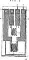
Wie aus den
Wie aus den
Wie in
Wie aus
Wie in
Wie in
Weiterhin ist, wie in
Die Attrappenmuster
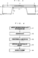
Als nächstes wird unter Bezugnahme auf die
Nunmehr erfolgt unter Bezugnahme auf die
Zuerst wird der Schritt S1 beschrieben.First, step S1 will be described.
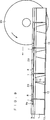
Die
Wie in
Dann wird, wie in
Dann werden, wie in
Als nächstes wird der Schritt S2 beschrieben.Next, the step S2 will be described.
Im Schritt S2 wird, wie in
Als nächstes wird der Schritt S3 beschrieben.Next, the step S3 will be described.
Im Schritt S3 werden, wie in
Als nächstes wird der Schritt S4 beschrieben.Next, the step S4 will be described.
Im Schritt S4 wird, wie in
Als nächstes wird der Schritt S5 beschrieben.Next, the step S5 will be described.
Im Schritt S5 wird, wie in
Bei dem Verfahren zur Herstellung von Wärme-Flussmesselementen gemäß dieser bevorzugten Ausführungsform werden daher die mehreren Dünnfilmsensorabschnitte
Die Parallelschaltungen der mehreren Wärmeerzeugungswiderstände
Weiterhin ermöglichen die Anschlüsse der Temperaturmesswiderstände
Die Attrappenmuster
Weiterhin werden im Schritt S1 die Attrappenmuster
Zwar wird bei der vorstehenden Beschreibung die Untersuchung der Abdeckung des Schutzfilms 3 im Schritt S4 nach der Stromversorgung im Schritt
Zweite bevorzugte Ausführungsform Second preferred embodiment
Bei dem Verfahren zur Herstellung von Wärme-Flussmesselementen gemäß der ersten bevorzugten Ausführungsform wurde die Untersuchung in Bezug auf Fehlstellen bei der Abdeckung mittels Stromzufuhr durchgeführt, während das Substrat
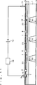
Unter Bezugnahme auf
Zuerst wird, wie im Schritt S1 der ersten, bevorzugten Ausführungsform, das Substrat
Dann wird, wie im Schritt S1 der ersten, bevorzugten Ausführungsform, nachdem ein Film aus Platin über der gesamten Oberfläche des Halterungsfilms
Dann wird unter Verwendung von Verfahren wie beispielsweise Dampfablagerung oder Sputtern ein Film aus Platin über der gesamten Oberfläche des Halterungsfilm
Dann werden Abschnitte des Schutzfilms
Dann wird, wie im Schritt S2 der ersten, bevorzugten Ausführungsform, ein Resist auf die gesamte Oberfläche des thermischen Oxidfilms
Dann werden, wie im Schritt S3 der ersten, bevorzugten Ausführungsform, leitfähige Stifte
Dann wird eine Untersuchung nach Fehlstellen der Abdeckung des Schutzfilms
Wie in
Dann wird, wie im Schritt S5 der ersten, bevorzugten Ausführungsform, das Substrat
Bei dem Verfahren zur Herstellung von Wärme-Flussmesselementen gemäß dieser bevorzugten Ausführungsform ermöglicht daher die Verwendung des leitfähigen Films
Da der voranstehend erwähnte, leitfähige Film
Zwar wird bei der voranstehenden Beschreibung die Untersuchung der Abdeckung des Schutzfilms
Claims (6)
Applications Claiming Priority (2)
| Application Number | Priority Date | Filing Date | Title |
|---|---|---|---|
| JP2004-139533 | 2004-05-10 | ||
| JP2004139533A JP4515143B2 (en) | 2004-05-10 | 2004-05-10 | Method for manufacturing thermal flow rate detection element |
Publications (2)
| Publication Number | Publication Date |
|---|---|
| DE102004052634A1 DE102004052634A1 (en) | 2005-12-08 |
| DE102004052634B4 true DE102004052634B4 (en) | 2012-04-19 |
Family
ID=35239924
Family Applications (1)
| Application Number | Title | Priority Date | Filing Date |
|---|---|---|---|
| DE102004052634A Expired - Fee Related DE102004052634B4 (en) | 2004-05-10 | 2004-10-29 | Method for producing heat flow measuring elements |
Country Status (4)
| Country | Link |
|---|---|
| US (1) | US6995028B2 (en) |
| JP (1) | JP4515143B2 (en) |
| KR (1) | KR100592177B1 (en) |
| DE (1) | DE102004052634B4 (en) |
Families Citing this family (3)
| Publication number | Priority date | Publication date | Assignee | Title |
|---|---|---|---|---|
| EP2682720B1 (en) * | 2011-03-02 | 2019-09-18 | Hitachi Automotive Systems, Ltd. | Heat-type flow meter |
| CN103649694B (en) * | 2011-07-13 | 2016-01-06 | 日立汽车系统株式会社 | Flowmeter |
| JP6475198B2 (en) * | 2016-06-29 | 2019-02-27 | 太陽誘電株式会社 | Variable capacitance device and antenna device |
Citations (5)
| Publication number | Priority date | Publication date | Assignee | Title |
|---|---|---|---|---|
| US3849872A (en) * | 1972-10-24 | 1974-11-26 | Ibm | Contacting integrated circuit chip terminal through the wafer kerf |
| US4426773A (en) * | 1981-05-15 | 1984-01-24 | General Electric Ceramics, Inc. | Array of electronic packaging substrates |
| US4855253A (en) * | 1988-01-29 | 1989-08-08 | Hewlett-Packard | Test method for random defects in electronic microstructures |
| DE19961129A1 (en) * | 1999-07-14 | 2001-02-01 | Mitsubishi Electric Corp | Thermic flow sensor, having heat-producing resistor pattern and temperature measuring film resistance arranged in planar arrangement on surface of substrate |
| US6225141B1 (en) * | 1999-09-03 | 2001-05-01 | Johnson Controls Technology Co. | Temperature sensor manufacturing process |
Family Cites Families (12)
| Publication number | Priority date | Publication date | Assignee | Title |
|---|---|---|---|---|
| JPS6397237U (en) * | 1986-12-12 | 1988-06-23 | ||
| US5389556A (en) * | 1992-07-02 | 1995-02-14 | Lsi Logic Corporation | Individually powering-up unsingulated dies on a wafer |
| US5532174A (en) * | 1994-04-22 | 1996-07-02 | Lsi Logic Corporation | Wafer level integrated circuit testing with a sacrificial metal layer |
| JPH10206205A (en) * | 1997-01-22 | 1998-08-07 | Ricoh Co Ltd | Manufacture for micro bridge sensor |
| US6744346B1 (en) * | 1998-02-27 | 2004-06-01 | Micron Technology, Inc. | Electronic device workpieces, methods of semiconductor processing and methods of sensing temperature of an electronic device workpiece |
| JP3513041B2 (en) * | 1999-01-25 | 2004-03-31 | 三菱電機株式会社 | Flow sensor |
| JP3461469B2 (en) * | 1999-07-27 | 2003-10-27 | 株式会社日立製作所 | Thermal air flow sensor and internal combustion engine controller |
| US6133054A (en) * | 1999-08-02 | 2000-10-17 | Motorola, Inc. | Method and apparatus for testing an integrated circuit |
| JP2001056310A (en) * | 1999-08-20 | 2001-02-27 | Sony Corp | Inspection of semiconductor device |
| JP4101518B2 (en) * | 2000-05-02 | 2008-06-18 | 株式会社日立製作所 | Air flow meter |
| JP5138134B2 (en) * | 2001-07-16 | 2013-02-06 | 株式会社デンソー | Thin film type sensor manufacturing method and flow sensor manufacturing method |
| US6844218B2 (en) * | 2001-12-27 | 2005-01-18 | Texas Instruments Incorporated | Semiconductor wafer with grouped integrated circuit die having inter-die connections for group testing |
-
2004
- 2004-05-10 JP JP2004139533A patent/JP4515143B2/en not_active Expired - Fee Related
- 2004-09-20 US US10/944,390 patent/US6995028B2/en active Active
- 2004-10-18 KR KR1020040083109A patent/KR100592177B1/en active IP Right Grant
- 2004-10-29 DE DE102004052634A patent/DE102004052634B4/en not_active Expired - Fee Related
Patent Citations (5)
| Publication number | Priority date | Publication date | Assignee | Title |
|---|---|---|---|---|
| US3849872A (en) * | 1972-10-24 | 1974-11-26 | Ibm | Contacting integrated circuit chip terminal through the wafer kerf |
| US4426773A (en) * | 1981-05-15 | 1984-01-24 | General Electric Ceramics, Inc. | Array of electronic packaging substrates |
| US4855253A (en) * | 1988-01-29 | 1989-08-08 | Hewlett-Packard | Test method for random defects in electronic microstructures |
| DE19961129A1 (en) * | 1999-07-14 | 2001-02-01 | Mitsubishi Electric Corp | Thermic flow sensor, having heat-producing resistor pattern and temperature measuring film resistance arranged in planar arrangement on surface of substrate |
| US6225141B1 (en) * | 1999-09-03 | 2001-05-01 | Johnson Controls Technology Co. | Temperature sensor manufacturing process |
Also Published As
| Publication number | Publication date |
|---|---|
| US20050250239A1 (en) | 2005-11-10 |
| DE102004052634A1 (en) | 2005-12-08 |
| JP2005321294A (en) | 2005-11-17 |
| US6995028B2 (en) | 2006-02-07 |
| KR20050107727A (en) | 2005-11-15 |
| JP4515143B2 (en) | 2010-07-28 |
| KR100592177B1 (en) | 2006-06-26 |
Similar Documents
| Publication | Publication Date | Title |
|---|---|---|
| EP1682882B1 (en) | Sensor arrangement provided with several potentiometric sensors | |
| DE69831600T2 (en) | ASSEMBLED SWITCHING MATRIX FOR CHECKING AND CONNECTING TO TESTING EQUIPMENT ON MEASURING DEVICES | |
| DE102010040224B4 (en) | A laminated gas sensor element, a gas sensor with a laminated gas sensor element, and a method of manufacturing a laminated gas sensor element | |
| DE602004010116T2 (en) | METHOD AND DEVICE FOR TESTING ELECTRICAL PROPERTIES OF AN OBJECT TO BE TESTED | |
| DE60030333T2 (en) | DEVICE FOR MEASURING A PHYSICAL SIZE, METHOD FOR THE PRODUCTION THEREOF, AND A VEHICLE CONTROL SYSTEM WITH THE APPARATUS FOR MEASURING A PHYSICAL SIZE | |
| DE19822123A1 (en) | Method and device for the detection of analytes | |
| DE102014200128B4 (en) | gas sensor element and gas sensor | |
| DE102015202176A1 (en) | gas detector | |
| DE69634233T2 (en) | Serial production of chips with coated selective electrodes | |
| DE102004052634B4 (en) | Method for producing heat flow measuring elements | |
| EP3271699B1 (en) | Device and process for characterizing a coolant | |
| DE102011076109A1 (en) | Semiconductor test method and apparatus and semiconductor device | |
| DE102006060113A1 (en) | Sensor and manufacturing process of a sensor | |
| DE102006022290B4 (en) | Heater with integrated temperature sensor on support | |
| EP0764334B1 (en) | Process for manufacturing components on a metal film base | |
| DE102015204023B4 (en) | Temperature sensitive element and temperature sensor | |
| WO2008000400A2 (en) | Method and device for testing the tightness of moisture barriers for implants | |
| DE1573802A1 (en) | Method for making defects in corrosion protection layers visible | |
| DE10314190A1 (en) | Thermosensitive flow rate detection element and method for its production | |
| DE2453578A1 (en) | PROCEDURE FOR DETERMINING COMPLETE THROUGH HOLES IN AN INSULATING LAYER APPLIED ON A CONDUCTIVE SUBSTRATE | |
| DE102011085747A1 (en) | Method for testing or adjusting thin-film-pH sensor present in medium, involves placing pH-sensitive element on substrate that emits signal depending on actual pH-value of medium | |
| DE102015204391A1 (en) | ELECTRONIC DEVICE AND METHOD FOR MANUFACTURING THE SAME | |
| DE602005003583T2 (en) | DEVICE AND METHOD FOR TESTING AT LEAST ONE CONDUCTIVE CONNECTION FOR FORMING AN ELECTRICAL CONNECTION BETWEEN AN ELECTRICAL COMPONENT AND A CONDUCTOR PLATE | |
| DE102005043271B4 (en) | Device for measuring the temperature in vertically structured semiconductor devices during operation and combined test structure for detecting the reliability | |
| EP0253420A1 (en) | Apparatus and process for electrochemical etching of silicon |
Legal Events
| Date | Code | Title | Description |
|---|---|---|---|
| OP8 | Request for examination as to paragraph 44 patent law | ||
| R016 | Response to examination communication | ||
| R016 | Response to examination communication | ||
| R018 | Grant decision by examination section/examining division | ||
| R020 | Patent grant now final |
Effective date: 20120720 |
|
| R084 | Declaration of willingness to licence | ||
| R119 | Application deemed withdrawn, or ip right lapsed, due to non-payment of renewal fee |