CN1662852B - Multi-tiered lithographic template - Google Patents
Multi-tiered lithographic template Download PDFInfo
- Publication number
- CN1662852B CN1662852B CN038141620A CN03814162A CN1662852B CN 1662852 B CN1662852 B CN 1662852B CN 038141620 A CN038141620 A CN 038141620A CN 03814162 A CN03814162 A CN 03814162A CN 1662852 B CN1662852 B CN 1662852B
- Authority
- CN
- China
- Prior art keywords
- layer
- patterning
- template
- patterned layer
- etch stop
- Prior art date
- Legal status (The legal status is an assumption and is not a legal conclusion. Google has not performed a legal analysis and makes no representation as to the accuracy of the status listed.)
- Expired - Fee Related
Links
Images


Classifications
-
- B—PERFORMING OPERATIONS; TRANSPORTING
- B82—NANOTECHNOLOGY
- B82Y—SPECIFIC USES OR APPLICATIONS OF NANOSTRUCTURES; MEASUREMENT OR ANALYSIS OF NANOSTRUCTURES; MANUFACTURE OR TREATMENT OF NANOSTRUCTURES
- B82Y10/00—Nanotechnology for information processing, storage or transmission, e.g. quantum computing or single electron logic
-
- G—PHYSICS
- G03—PHOTOGRAPHY; CINEMATOGRAPHY; ANALOGOUS TECHNIQUES USING WAVES OTHER THAN OPTICAL WAVES; ELECTROGRAPHY; HOLOGRAPHY
- G03F—PHOTOMECHANICAL PRODUCTION OF TEXTURED OR PATTERNED SURFACES, e.g. FOR PRINTING, FOR PROCESSING OF SEMICONDUCTOR DEVICES; MATERIALS THEREFOR; ORIGINALS THEREFOR; APPARATUS SPECIALLY ADAPTED THEREFOR
- G03F7/00—Photomechanical, e.g. photolithographic, production of textured or patterned surfaces, e.g. printing surfaces; Materials therefor, e.g. comprising photoresists; Apparatus specially adapted therefor
- G03F7/0017—Photomechanical, e.g. photolithographic, production of textured or patterned surfaces, e.g. printing surfaces; Materials therefor, e.g. comprising photoresists; Apparatus specially adapted therefor for the production of embossing, cutting or similar devices; for the production of casting means
-
- B—PERFORMING OPERATIONS; TRANSPORTING
- B82—NANOTECHNOLOGY
- B82Y—SPECIFIC USES OR APPLICATIONS OF NANOSTRUCTURES; MEASUREMENT OR ANALYSIS OF NANOSTRUCTURES; MANUFACTURE OR TREATMENT OF NANOSTRUCTURES
- B82Y40/00—Manufacture or treatment of nanostructures
-
- G—PHYSICS
- G03—PHOTOGRAPHY; CINEMATOGRAPHY; ANALOGOUS TECHNIQUES USING WAVES OTHER THAN OPTICAL WAVES; ELECTROGRAPHY; HOLOGRAPHY
- G03F—PHOTOMECHANICAL PRODUCTION OF TEXTURED OR PATTERNED SURFACES, e.g. FOR PRINTING, FOR PROCESSING OF SEMICONDUCTOR DEVICES; MATERIALS THEREFOR; ORIGINALS THEREFOR; APPARATUS SPECIALLY ADAPTED THEREFOR
- G03F1/00—Originals for photomechanical production of textured or patterned surfaces, e.g., masks, photo-masks, reticles; Mask blanks or pellicles therefor; Containers specially adapted therefor; Preparation thereof
- G03F1/68—Preparation processes not covered by groups G03F1/20 - G03F1/50
-
- G—PHYSICS
- G03—PHOTOGRAPHY; CINEMATOGRAPHY; ANALOGOUS TECHNIQUES USING WAVES OTHER THAN OPTICAL WAVES; ELECTROGRAPHY; HOLOGRAPHY
- G03F—PHOTOMECHANICAL PRODUCTION OF TEXTURED OR PATTERNED SURFACES, e.g. FOR PRINTING, FOR PROCESSING OF SEMICONDUCTOR DEVICES; MATERIALS THEREFOR; ORIGINALS THEREFOR; APPARATUS SPECIALLY ADAPTED THEREFOR
- G03F7/00—Photomechanical, e.g. photolithographic, production of textured or patterned surfaces, e.g. printing surfaces; Materials therefor, e.g. comprising photoresists; Apparatus specially adapted therefor
- G03F7/0002—Lithographic processes using patterning methods other than those involving the exposure to radiation, e.g. by stamping
-
- G—PHYSICS
- G03—PHOTOGRAPHY; CINEMATOGRAPHY; ANALOGOUS TECHNIQUES USING WAVES OTHER THAN OPTICAL WAVES; ELECTROGRAPHY; HOLOGRAPHY
- G03F—PHOTOMECHANICAL PRODUCTION OF TEXTURED OR PATTERNED SURFACES, e.g. FOR PRINTING, FOR PROCESSING OF SEMICONDUCTOR DEVICES; MATERIALS THEREFOR; ORIGINALS THEREFOR; APPARATUS SPECIALLY ADAPTED THEREFOR
- G03F7/00—Photomechanical, e.g. photolithographic, production of textured or patterned surfaces, e.g. printing surfaces; Materials therefor, e.g. comprising photoresists; Apparatus specially adapted therefor
- G03F7/0035—Multiple processes, e.g. applying a further resist layer on an already in a previously step, processed pattern or textured surface
Abstract
This invention relates to semiconductor devices, microelectronic devices, microelectromechanical devices, microfluidic devices, photonic devices, and more particularly to a multi-tiered lithographic template, a method of forming the multi-tiered lithographic template and a method for forming devices with the multi-tiered lithographic template. The multi-tiered lithographic template (10/10') is formed having a first relief structure and a second relief structure, thereby defining a multi-tiered relief image. The template is used in the fabrication of a semiconductor device (40) for affecting apattern in device (40) by positioning the template in close proximity to semiconductor device (40) having a radiation sensitive material formed thereon and applying a pressure to cause the radiation sensitive material to flow into the multi-tiered relief image present on the template. Radiation is then applied through the multi-tiered template so as to further cure portions of the radiation sensitive material and further define the pattern in the radiation sensitive material. The multi-tiered template is then removed to complete fabrication of semiconductor device (40).
Description
Technical field
The present invention relates to semiconductor devices, microelectronic component, micro electro mechanical device, microfluidic device, photonic device, relate more specifically to the method that a kind of Lithographic template, a kind of formation comprise the Lithographic template of sandwich construction (multi-tiered), and a kind of method of using the multilayer Lithographic template to form device.
Background technology
The manufacturing of integrated circuit relates to the interactional in some way several layer materials of production.One or more layers can be patterned in these layers, makes the zones of different of described layer have different electrology characteristics, and they can interconnect in layer or with other layer, thereby produce electricity device and circuit.These zones can produce by optionally introducing or remove various materials.Limiting these regional patterns produces by photoetching method usually.For instance, coating one deck photoresist material on the layer of wafer substrate.Use photomask (comprising printing opacity and light tight district) to come optionally, for example the form exposure photo-etching glue material of ultraviolet light, electron beam or X ray by radiation.Remove or be exposed to the photoresist material of radiation by using developer, perhaps be not exposed to the material of radiation.
Then, on the layer of not protected, use etching, and when removing resist, the layer that covers substrate is patterned by residual resist.
Typically use for example above-mentioned photoetching method that the design transfer of photomask is become device.Along with feature on the semiconductor devices (feature) size reduces greatly from the scope of sub-micrometer range to 100 nanometer, need new photoetching method or technology to come the highdensity semiconductor devices of patterning.Advised severally can realizing this demand and based on the new photoetching technique of impression (imprinting) and seal (stamping).The spy has shown that stepping flash type imprint lithography (Step and Flash Imprint Lithography) (SFIL) can patterning carefully reaches the line of 20 nanometers.
The SFIL template is typically made by the chromium of coating one deck 80-100 nanometer thickness on transparent quartz plate.On chromium, apply resist layer, and use electron beam or optical exposure system patterning.Then, resist is put into developer, on the chromium layer, form pattern.Use resist as mask, the etching chromium layer.Then, the chromium layer is as the hard mask of etching quartz plate.At last, remove the layer that dechromises, thereby on quartz, form the quartz template that comprises relief image.
Generally speaking, the SFIL technology is benefited from its unique photochemistry use, environment for use temperature and is implemented the required low pressure of SFIL process.During typical SFIL process, with organic plane layer coated substrate, and make it very near transparent SFIL template, this template typically is made up of quartz, and comprises relief image and be coated with the material of low-surface-energy.The photocuring organic solution of deposition ultraviolet or extreme ultraviolet sensitivity between the substrate of template and coating.Use minimum pressure, template and substrate, and contact with the organic layer of photocuring more specifically.Then, at room temperature solidify or crosslinked organic layer by the irradiation template.Light source typically uses UV radiation.But according to the photosensitivity of template and photocuring organic layer, wavelength coverage (150 nanometers-500 nanometer) is fine.Then, separate template with organic layer, on plane layer, stay the organic duplicate of relief printing plate of template from substrate.Then, use short halogen to penetrate (short halogen break-through), come the described pattern of etching by oxygen reactive ion etching (RIE) again, on organic layer and plane layer, form the feature of high-resolution, high-aspect-ratio.
Should note the difference between mask and the Lithographic template.Mask has the pattern of being made up of opaque and transparent region, and makes the space image of light enter the photoresist material as masterplate.Lithographic template has the relief image that is etched in its surface, produces a kind of shape or model.In SFIL, when optical solidified liquid flows in the relief image and solidifies subsequently, form pattern.Therefore, the necessary attribute of mask and template is very different.
Shown that the SFIL technology can differentiate the feature that reaches 20 nanometers for a short time.Therefore, can on a wafer, draw the number of characteristics size.Yet also there are some problems in this above-mentioned SFIL template fabrication.Although the problem of a prior art processes is to produce uniform feature on the size, can not use the SFIL technology to produce the layer structure of bidimensional.Typically, use the SFIL technology only to form single tier templates, wherein one deck is dark, therefore thinks only have one " layer ".Use in many kinds, comprise the structure that needs to produce multilayer in microelectronics or the MEMS application.In addition, this sandwich construction provides a kind of stratiform resist side, is used for the formation of T door, diffraction optical element, grating coupler and other structure.
When only using the hard mask of chromium, also there is problem about the quartz template uniform etching.It should be noted that the etch depth on the template finally determined the thickness of photocuring resist layer on the wafer, therefore is very crucial.More specifically, aspect etch uniformity, exist little feature (<200 nanometer) to go up the problem of micro loading effect.Known little (<200 nanometer) bigger feature of feature etching is slower, and this just causes the unevenness aspect the etch depth of critical dimension and whole template.Because the micro loading effect during the etching, the etching fully of little feature can not be equally dark as big feature etching.This just causes the thickness uneven resist image of feature from big to small.Therefore, produce three specific negative structures: (i) bad live width is controlled; (ii) uneven etch depth (causing bad resist thickness evenness); Reach the (iii) resist section of sphering.
In addition, exist the electron beam of template to write and make the problem of rear pattern plate inspection aspect.Specifically, the accumulation of electric charge must provide conductive layer during the electron beam exposure.In addition, because template is made up of homogenous material, be not easy to realize auditability.Typically check system makes and uses up (ultraviolet or extreme ultraviolet light), and perhaps electronics is determined characteristic dimension, and in the unwanted defective of template detection.Need and there be the difference of reflection or refractive index in the light based system at the patterning of template between the patterned area, thereby the preferable image contrast is provided.In addition, need and there be the difference of atomic number in the electronics based system at the patterning of template between the patterned area.In order to overcome described problem, multiple material with different optical character or different atomic numbers allows to check, and also is necessary to inferior 100 nanofeature.
Therefore, it is favourable providing a kind of template that can make sandwich construction.
An object of the present invention is to provide a kind of improved multilayer Lithographic template, a kind of method of making described improved multilayer Lithographic template, and a kind ofly use the described improved multilayer Lithographic template that can realize sandwich construction to make the method for semiconductor devices.
An object of the present invention is to provide a kind of improved multilayer Lithographic template, a kind of method of making described improved multilayer Lithographic template, and a kind ofly use the described improved multilayer Lithographic template that can check submicrometer structure to make the method for semiconductor devices.
Summary of the invention
The application relates to semiconductor devices, microelectronic component, micro electro mechanical device, microfluidic device, photonic device, and relate more specifically to a kind of Lithographic template, a kind of method that forms the multilayer Lithographic template, and a kind of method of using the multilayer Lithographic template to form device.The invention discloses a kind of multilayer Lithographic template that comprises the relief structure of substrate and a plurality of formation sandwich constructions.Described multilayer Lithographic template forms as follows: provide wherein or be formed with the transparent substrates of first patterned relief structure and additional patterned relief structure on the upper space, thereby limit the multilayer Lithographic template.The lithographic patterning technology of use standard, but perhaps directly use imaging ground dielectric process technology to form the relief structure of a plurality of patternings alternatively.
In addition, a kind of method of using the multilayer Lithographic template that is provided to make device is provided the application, it may further comprise the steps: thus provide substrate, to applying radiation-sensitive materials on the Semiconductor substrate, the disclosed multilayer Lithographic template in front is provided, settle the multilayer Lithographic template to contact with radiation-sensitive materials, on radiation-sensitive materials, produce pattern, make radiation see through the multilayer Lithographic template to exerting pressure on the template, at least a portion radiation-sensitive materials on the exposure substrate, thereby further influence the pattern of radiation-sensitive materials, and remove the multilayer template from substrate.
Description of drawings
In conjunction with the accompanying drawings, from following detailed description of preferred embodiments, those skilled in the art will be more readily understood aforementioned and other and purpose and advantage more specifically of the present invention, wherein:
Fig. 1-7 has set forth the step of making according to first open technology of multilayer Lithographic template of the present invention in the cut-open view mode.
Fig. 8-11 has set forth the step of making according to second open technology of multilayer Lithographic template of the present invention in the cut-open view mode.
Figure 12-16 has set forth the step of making according to the 3rd open technology of multilayer Lithographic template of the present invention in the cut-open view mode.
Figure 17 is to use the simplification process chart of making semiconductor devices according to multilayer Lithographic template of the present invention.
Should understand for the simplification of setting forth and clear, the element of setting forth in the accompanying drawing does not need to draw in proportion.
For instance, for clarity, some size of component has been exaggerated with respect to other element.In addition, under suitably considering,, repeated reference number in the accompanying drawings in order to show corresponding or similar elements.
Embodiment
The present invention relates to make the multilayer Lithographic template that is used for stepping flash type imprint lithography (SFIL).Advise deposit multilayer material on substrate surface herein, thereby form the multilayer Lithographic template.Disclosure expection according to the present invention comprises use as the described standard photolithographic steps of Fig. 1-7 according to the method for formation multilayer Lithographic template of the present invention, forms the multilayer Lithographic template but perhaps use as the described directly imaging dielectric process technology of Fig. 8-11.Expect also that according to disclosure of the present invention the combination that can use disclosed method according to the present invention forms the multilayer Lithographic template.
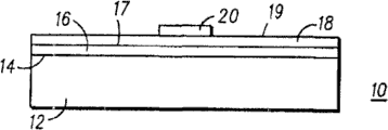
Specifically, illustrated and made according to first step in first technology of multilayer Lithographic template 10 of the present invention with reference to Fig. 1.Illustrated is the substrate 12 that has surface 14.Disclosed substrate 12 is by transparent material, for example quartz material, makrolon material, Pyrex glass material, calcium fluoride (CaF
2) material, magnesium fluoride (MgF
2) material, perhaps the light transmissive material of any other similar type is formed.Substrate 12 is formed by transparent material, and the passage of light is provided.
As described in Figure 1, on substrate 12 surfaces 14, deposit first etch stop layer 16.First etch stop layer 16 is by silicon nitride (SiN), silicon dioxide (SiO
2), chromium (Cr), chromium oxide (CrO), aluminium oxide (AlO), aluminium nitride (AlN), chromium nitride (CrN), tin indium oxide (ITO), indium oxide (InO), tin oxide (SnO), zinc paste (ZnO), cadmium oxide (CdO), cupric oxide aluminium (CuAlO), cupric oxide gallium (CuGaO), cadmium tin (CdSnO), perhaps any other transparent or translucent material, and their combination forms.Be to be understood that working as some material is used for substrate 12, during with first patterned layer that needs particular etching process (situation of current discussion), first etch stop layer 16 is chosen wantonly, and first patterned layer (situation of current discussion) directly is deposited on the surface 14 of substrate 12.
Referring now to Fig. 2, substrate 12 is described, it deposits first etch stop layer 16, first patterned layer 18 and patterning resist layer 20 above surface 14.Depend on whole design object, and the material that comprises of first etch stop layer 16, disclosed first patterned layer 18 is formed by opaque or material transparent (situation of current discussion).More specifically, the particular type of the open material therefor of the application is concerning and must bear the processing step as a result of making template 10 fully.On the surface 17 of first etch stop layer 16, form first patterned layer 18 that has surface 19 by methods such as spin coating, sputter, steam depositions.
Disclosed first patterned layer 18 usually by be used for the material that first etch stop layer 16 has different reflectivity (or refractive index) or different atomic numbers and form.The difference of this atomic number provides improved auditability matter, as described in the present application.The transparent material of disclosed suitable manufacturing first patterned layer 18 is silicon dioxide (SiO
2), silicon nitride (SiN), silicon-oxygen nitride (SiON), tin indium oxide (ITO) etc.The opaque material of disclosed suitable manufacturing first patterned layer 18 is tungsten (W), tungsten silicide (WSi), tungsten nitride silicon (WSiN), tungalloy, tantalum (Ta), tantalum silicide (TaSi), tantalum nitride silicon (TaSiN), tantalum alloy, titanium (Ti), titanium alloy, molybdenum (Mo), molybdenum silicide (MoSi), molybdenum alloy, gold (Au), chromium (Cr) etc.Substrate self as previously mentioned, should be understood that some patterned layer does not need etch stop layer, because can be used as the etching barrier material fully.During electron beam writes, can use first patterned layer 18 to come assist charge dissipation.In addition, owing to use different materials in multilayer, first patterned layer 18 helps the template inspection based on SEM.The thickness of disclosed first patterned layer 18 depends on the required length breadth ratio that will be embossed in the photocuring resist layer usually.Specifically, first patterned layer 18 need have enough physical strengths and durability, thereby is producing under the relevant stress with template, and can survive during the Lithographic template that is used to complete is made semiconductor devices subsequently.Therefore, disclosed patterned layer 18 has the thickness between 10 and 5000 nanometers usually, and preferred thickness is at least 50 nanometers.
The resist layer 20 of patterning is patterned on the upper space 19 of first patterned layer 18, and is used for patterning first patterned layer 18 subsequently.As described in Figure 2, the resist layer 20 of patterning comes patterning by standard light or electron beam patterning technique.Resist layer 20 typical cases of patterning for example are patterned formation by known standard photoresist or electron sensitive resist material in the technology, thereby are used as the organic polymer with the mask of after etching first patterned layer 18.
During making multilayer Lithographic template 10, photoresist layer 20 is as the mask of etching first patterned layer 18.As described in Figure 3, first patterned layer 18 is etched on the surface 17 of first etch stop layer 16, thereby exposes the part 22 of first etch stop layer 16.The etching of first patterned layer 18 is finished by the wet method or the dry etch technique of standard.At last, remove resist layer 20, expose first patterned layer 24, it has surface 25 and has as described in Figure 3 size " x ", and wherein " x " depends on the final application of multilayer Lithographic template 10.
Referring now to Fig. 4, then on the part 22 of first patterned layer 24 and first etch stop layer 16 that exposes, deposit second etch stop layer 26.The bent opaque or material transparent of disclosed second etch stop layer 26 forms, and depends on the deposition of overall design objective and subsequent layer.More specifically, the particular type of the open material therefor of the application is concerning and must carry out the final processing step of making template 10 to finish.Expect that also second etch stop layer 26 can choose wantonly according to forming the concrete material that front layer and back layer use.In the situation that does not need second etch stop layer 26, second patterned layer (situation of current discussion) will be formed on the surface of first patterned layer 24 directly.
The transparent material of disclosed suitable manufacturing second etch stop layer 26 is chromium oxide (Cr
xO
y), aluminium oxide (Al
xO
y), aluminium nitride (Al
xN
y), chromium nitride (Cr
xN
y), silicon dioxide (SiO
2), chromium (Cr), tin indium oxide (ITO), indium oxide (In
xO
y), tin oxide (SnO), zinc paste (ZnO), cadmium oxide (CdO), cupric oxide aluminium (CuAlO), cupric oxide gallium (CuGaO), cadmium tin (CdSnO), silicon nitride (SiN), the combination of these materials, perhaps any other transparent or translucent material etc., wherein " x " and " y " is positive, the relative content of element in the expression aforesaid compound.In preferred embodiments, the x scope is 0.1 to 1.0, and the y scope is 0.1 to 1.0.In an example, the oxide of stoichiometric proportion is Al
2O
3But those skilled in the art realizes depositing the aluminum oxide film of non-stoichiometric, and is used as identical purpose with the film of stoichiometric proportion.The opaque material of disclosed suitable manufacturing second etch stop layer 26 is a chromium (Cr) etc.Form second etch stop layer 26, help the patterning of rest layers subsequently.The thickness of disclosed second etch stop layer 26 depends on the etching selectivity to patterned layer, and the charge conductivity of material therefor.Specifically, in order to overcome any micro loading effect, need enough low etch-rate with respect to patterned layer second etch stop layer 26.In addition, second etch stop layer 26 must have enough intensity, thereby is producing under the relevant stress with template, and can survive during the Lithographic template that is used to complete is made semiconductor devices subsequently.Therefore, the thickness of common disclosed second etch stop layer 26 is in the scope of 1-1000 nanometer, and preferred thickness is at least 5 nanometers.On the surface 25 of first patterned layer 24, form second etch stop layer 26 that has surface 27 by methods such as spin coating, sputter, steam depositions.
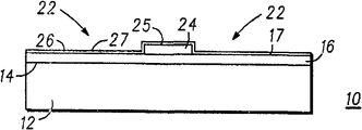
Referring now to Fig. 5, substrate 12 is described, deposit first etch stop layer 16, first patterned layer 24 and second etch stop layer 26 above it.Additional second patterned layer 28 that forms on the surface 27 of second etch stop layer 26.Depend on whole design object, and the material that comprises of second etch stop layer 26, disclosed second patterned layer 28 is formed by opaque or material transparent.More specifically, the particular type that the invention discloses material therefor is concerning and must carry out the final processing step of making template 10 to finish.
Disclosed first patterned layer 18 (previous introduce) and second patterned layer 28 are common by forming with the material that the material that is used for following first etch stop layer 16 or second etch stop layer 26 has different reflectivity (or refractive index) or different atomic numbers respectively.The difference of this atomic number provides improved auditability matter, as described herein.The transparent material of disclosed suitable manufacturing second patterned layer 28 is silicon dioxide (SiO
2), silicon nitride (SiN), silicon-oxygen nitride (SiON), tin indium oxide (ITO) etc.The opaque material of disclosed suitable manufacturing first patterned layer 18 and second patterned layer 28 is tungsten (W), tungsten silicide (WSi), tungsten nitride silicon (WSiN), tungalloy, tantalum (Ta), tantalum silicide (TaSi), tantalum nitride silicon (TaSiN), tantalum alloy, titanium (Ti), titanium alloy, molybdenum (Mo), molybdenum silicide (MoSi), molybdenum alloy, gold (Au), chromium (Cr) etc.During electron beam writes, can use first patterned layer 18 and second patterned layer 28 to come assist charge dissipation.In addition, because the electron scattering characteristic of the different materials that uses in multilayer, patterned layer 18 and 28 helps the template inspection based on SEM.In addition, similar to first patterned layer 18, the thickness of disclosed second patterned layer 28 has usually and depends on the required length-diameter ratio that will be embossed into the photocuring resist layer.Specifically, second patterned layer 28 need have enough physical strengths and durability, thereby is producing under the relevant stress with template, and can survive during the Lithographic template that is used to complete is made semiconductor devices subsequently.Therefore, disclosed second patterned layer 28 has the thickness between 10 and 5000 nanometers usually, and preferred thickness is at least 50 nanometers.On the surface 27 of second etch stop layer 26, form second patterned layer 28 that has surface 29 by methods such as spin coating, sputter, steam depositions.
Referring now to Fig. 6 and 7, substrate 12 is described, second patterned layer 28 that be formed with surface 14, first etch stop layer 16 above it, on second etch stop layer 26 that forms on first patterned layer 24 that forms on the surface 17 of first etch stop layer 16, the surface 25, surface 27, forms, and the patterning resist layer 30 that on the surface 29 of second patterned layer 28, forms at second etch stop layer 26 in first patterned layer 24.More specifically, what form on the surface 29 of second patterned layer 28 is resist layer 30, and as described in Figure 6, it comes patterning by the optics or the electron beam patterning technique of standard.Resist layer 30 is typically by known standard photoresist or electron sensitive resist material in the technology, and the organic polymer that for example is patterned forms, thereby as the mask with after etching second patterned layer 28.
During manufacture, photoresist layer 30 is as the mask of etching second patterned layer 28.As described in Figure 7, second patterned layer 28 is etched on the surface 27 of second etch stop layer 26, thereby exposes the part 32 of second etch stop layer 26.The etching of second patterned layer 28 is finished by the wet method or the dry etch technique of standard.Then, if desired, over etching second patterned layer 28 provides improved homogeneity, and 26 places stop at second etch stop layer.
At last, in order to finish multilayer template 10, remove resist layer 30, expose have size second patterned layer 34 of " y ", wherein the size of first patterned layer 24 " x " is greater than the size " y " of second patterned layer 24 (x>y).In the situation that second etch stop layer 26 is formed by opaque material, need remove the expose portion 32 (as described in Figure 7) of second etch stop layer 26, thereby allow the path of radiation subsequently by wherein.With the mode that comprises opaque second etch stop layer 26 and second patterned layer 28 make multilayer Lithographic template 10 and provide the auditability that minimizes, strengthens of unwanted remaining photopolymer, with compatibility, anti-erosion cleaning, the fidelity of required pattern and the amorphous/low surface roughness material of transfer characteristics when the front template recovery technique, and owing to change material layer improved template contrast.
Fig. 7 has set forth the multilayer Lithographic template 10 that comprises substrate 12 in the cut-open view mode, substrate 12 has surface 14, covering is pressed in first etch stop layer 16 above the surface 14 of substrate 12, first patterned layer 24 with surface 25 and size " x ", and cover second patterned layer 34 above the surface 27 of second etch stop layer 26 with size " y ", wherein " x " is greater than " y ".When finishing, template 10 defines multilayer relief image 36 wherein.Be to be understood that the application's disclosure expectation manufacturing also comprises that the patterned layer of additional stacks has more than two-layer relief image with qualification when describing when having the two-layer relief image 36 that is limited by first patterned layer 24 and second patterned layer 34.In needing the situation of extra play, repeat foregoing patterning step.
Referring now to Fig. 8-11, in the cut-open view mode of simplifying the step of making the multilayer Lithographic template is described, wherein use imageable dielectric process technology during manufacture.All parts similar to assembly described in Fig. 1-7 that should be noted that Fig. 8-11 are with similar numeral, and add that single apostrophe represents different embodiments.
Disclosure comprises resist, perhaps once was patterned, but as the patterned layer with the middle layer of design transfer to the second layer.Behind patterning, in fact described patterned layer becomes final template relief structure.By correctly using the unique material of the required strong engineering properties of the patternable characteristic made up photoresist and template relief layer, this is possible.These character comprise high bond strength, the high mode high shear strength to substrate, and good thermotolerance.For example hydrogen silsesquioxane (hydrogen silsesquioxane) material (HSQ) be patternable and have very high resolution, and solidify the back and form the highly stable silicon dioxide that is suitable for as the impression block relief structure.Can replace using HSQ with material with similar characteristic.But, should be noted that anyly thisly to be radiosensitive and can be patterned to have material as the suitable physical character of template relief layer again and be unique and be key of the present invention.
Referring now to Fig. 8, substrate 12 ' is described, its substrate 12 similar formation common and Fig. 1-7.In a preferred embodiment, disclosed first patterned layer 18 ' is formed by imageable dielectric substance.More specifically, disclosed patterned layer is formed by imageable oxide, and for example Dow Corning is with FOX-
 The hydrogen silsesquioxane of selling (HSQ).In addition, patterned layer 18 ' can be formed by optional dielectric substance, for example imageable nitride, perhaps imageable oxynitride.During making template, go up formation patterned layer 18 ' on the surface 14 ' of substrate 12 ', then at low temperature, under about 160 ℃, cure, remove the solvent of any existence.
Fig. 8 illustrates substrate 12 ', is formed with surface 14 ', patterned layer 18 ' above it.After having cured patterned layer 18 ', light by standard or electron beam patterning techniques exposure template layer 18 ', thus form first patterned layer that is of a size of " x ", but the perhaps imaging relief structure 24 ' of patterning, as described in Figure 9.Electron beam irradiation, X-radiation, deep ultraviolet radiation, ion beam irradiation are used in the expectation of the application's disclosure, perhaps any exposure that other can provide the suitable radiation of patterned layer 18 ' exposure to come complete layer 18 '.First patterned layer 18 ' is radiated through on the surface 14 ' of substrate 12 '.Then, washing patterned layer 18 ' in developer is if imageable layer is a negative effects, by removing the unexposed of patterned layer 18 ' or radiant section not; If perhaps imageable layer is the positivity effect, produce pattern by removing exposure region, thereby to cause the imageable relief layer 24 ' of residue as described in Figure 9.
The application's disclosure also is desirably in as described in Figure 8 the template 10 ' and comprises etch stop layer 21.In the case, etch stop layer is preferably formed on the surface 14 ' of substrate 12 ', is clipped between the substrate 12 ' and first patterned layer 18 '.Alternatively, etch stop layer 21 can be formed in 10 ' layer of the template Anywhere.Etch stop layer 21 will be used as charge dissipation layer according to the material type of its composition when being formed by conductive material, perhaps be used as contrast enhancing layer when being formed by dielectric substance.When etch stop layer 21 was used for the charge dissipation purpose, it was by being characterized as during the template manufacturing dissipation electric charge and being used for realizing that the conductive material of electron beam exposure and inspection forms.More specifically, disclosed etch stop layer with charge dissipation character is formed by following conductive material: aluminium (Al), copper (Cu), titanium (Ti), chromium (Cr), indium oxide (InO
2), tin oxide (SnO
2), tin indium oxide (ITO),, zinc paste (ZnO
2), cadmium oxide (CdO), cupric oxide aluminium (CuAlO), cupric oxide gallium (CuGaO), cadmium tin (CdSnO), polyaniline (polyanaline), perhaps any other can be from patterned layer selectivity remove and the conductive material of the electric charge that is used for dissipating.The disclosed etch stop layer 21 that forms as charge dissipation layer has the minimum thickness that depends on the material therefor charge conductivity.Formation has the etch stop layer 21 of charge dissipation character, writes at electron beam, perhaps is used for helping the dissipation electric charge during other radiation (situation of current discussion) of the described layer of pattern.
When formation etch stop layer 21 was used for the contrast enhancing, disclosed material was formed by the material with optical check character.More specifically, disclosed have the enhanced propertied etch stop layer of contrast by silicon nitride (SiN), silicon dioxide (SiO
2), chromium oxide (Cr
xO
y), aluminium oxide (Al
xO
y), aluminium nitride (Al
xN
y), chromium nitride (Cr
xN
y), perhaps any other has the enhanced propertied material of contrast that allows optical check template 10 ' and forms.
Disclosed etch stop layer 21 has the thickness in the 1-1000 nanometer range usually, and preferred thickness is at least 5 nanometers.Etch stop layer 21 waits and forms by spin coating, sputter, steam deposition.In the described specific embodiments of Fig. 8, the electric charge etch stop layer 21 that is deposited on above the patterned layer 18 ' is formed by aluminium (Al), thereby shows charge dissipation character.
No matter the application's disclosure expectation when beamwriter lithography, optical check etc. needs, can comprise other material in template 10 ', and the method that strengthens as charge dissipation or contrast.These materials can form extremely thinly, and can not reduce resolution because of the interference emission source.Because need remove the metal core etch stop layer subsequently, for easy to process, selecting the standard of etch stop layer is to remove easily.Use wet method or dry technique to remove described layer.But,, must from patterned relief layer, remove in the high selectivity mode in order to keep the high resolving power of gained patterned relief layer.Aluminium (Al) is that conduction and selectivity can be removed an example of material, be applied to 100 to
 The time, it can be removed by the aqueous base developers of routine.
Referring now to Figure 10 explanation first patterned layer 24 ' upper space 25 ' on deposition second patterned layer 28 '.In preferred embodiments, disclosed second patterned layer 28 ' form by imageable dielectric substance.More specifically, to first patterned layer 18 ' similar, disclosed second patterned layer 28 ' formed by imageable oxide, for example Dow Corning is with FOX-
 The hydrogen silsesquioxane of selling (HSQ).In addition, but second patterned layer 28 ' can form for example imageable nitride, perhaps imageable oxynitride by optional imaging dielectric substance.During making template, first patterned layer 24 ' surface 25 ' on form second patterned layer 28 ', then at low temperature, under about 160 ℃, cure, remove the solvent of any existence.Then, washing patterned
 layer 28 in developer ', if imageable layer is a negative effects, by removing the unexposed of patterned layer 18 ' or radiant section not; If perhaps imageable layer is the positivity effect, produce pattern by removing exposure region, thereby cause remaining second patterned layer, but or the imaging relief layer 34 of patterning ', as described in Figure 11.
Be to be understood that make template 10 ' during, but can in the chemical reaction of image forming material, use chemistry to amplify, reach the demand of hanging down radiation.More specifically, in the chemistry of suggestion amplifies, first patterned layer 18 ' or the 28 ' radiation of second patterned layer after, usually, but be not the essential second step baking step that uses.In addition, can use de-sludging technology, comprise light plasma etch, after forming relief structure, remove any residual transparent dielectric material, and specifically, any want residual residual first patterned layer 18 in clear area ' or second patterned layer 28 '.
Figure 11 with the cut-open view mode set forth comprise substrate 12 ' the whole printing stencils 10 ' of multilayer lithographic plate, substrate has surface 14 ', has first patterned layer 24 ' of surface 25 ' and size " x ", and cover first patterned layer 24 ' surface 25 ' above second patterned layer 34 ' with size " y ", wherein " x " is greater than " y ".When finishing, template 10 ' defines multilayer relief image 36 ' wherein.Be to be understood that the application's disclosure expects that manufacturing also comprises that the patterned layer of additional stacks has more than two-layer relief image with qualification when describing when having relief image two-layer and that is limited by first patterned layer 24 ' and second patterned layer 34 ' 36 '.
In addition, the manufacturing of the application's disclosure expectation multilayer Lithographic template comprises two disclosed technology in front, wherein use as the front and form a part of template layer, but and use as the front and form a part of template layer with reference to the described directly imaging dielectric process technology of Fig. 8-11 with reference to the described standard photoetching of Fig. 1-7 process technology.More specifically, expectation produces the multilayer Lithographic template, wherein use as the front and form first patterned layer with reference to the described standard photoetching of Fig. 1-7 process technology, and but use forms second patterned layer as the front with reference to the described directly imaging dielectric process technology of Fig. 8-11, perhaps opposite, depend on that the purpose of the template of finishing is used.
Also disclose the application's expectation in addition and randomly comprised the stress compensation layer (not shown) that is clipped between the layer that comprises structure 10 or 10 ', be used in the counteracting face and/or face twists outward.More specifically, the application expectation comprises the stress compensation layer that is positioned at any position of template layer, for example on arbitrary of first etch stop layer 16 on first patterned layer 24, perhaps Lin Jin substrate 12 ' on, as described in Figure 11.In optional preferred embodiment, stress compensation layer will be clipped between the substrate 12 and first etch stop layer 16.In the situation that has comprised stress compensation layer, expect that it will be formed by oxide, nitride, oxynitride, concrete as Si
xO
y, Si
xN
y, SiON, perhaps tin indium oxide (ITO), indium oxide (InO
2), tin oxide (SnO
2), zinc paste (ZnO
2), cadmium oxide (CdO
2), cupric oxide aluminium (CuAlO), cupric oxide gallium (CuGaO), cadmium tin (CdSnO), perhaps any other transparent or semitransparent conductive material, and their combination.Stress compensation layer be for offset to comprise structure 10/10 ' any power of applying of layer, cause the bow action of described layer, perhaps cause the distortion of the feature that forms in " x ", " y " or " z " plane.The thickness of stress compensation layer will be from 5 nanometers to 5 micron, and typical thickness is 200 nanometers.Described thickness can be according to the character and the type of the film that is deposited, and the demand of membrane stress compensation is regulated.
In addition, as described in Figure 11, when substrate 12 ' surface 13 on when settling stress compensation layer 38, can realize the further advantage of stress compensation layer, illustrate with layer 38.Except being used as foregoing stress compensation layer, present stress compensation layer 38 permission static maintenance templates 10 '.Electrostatic clamp (maintenance) template 10 ' in ablation process, limit template 10 ' move, and also guaranteed template 10 during photolithographic exposure ' be held smooth.
Figure 12-16 has illustrated the step that forms another optional method again of multilayer Lithographic template of the present invention.All parts that should be understood that Figure 12-16 similar to the described assembly of Fig. 1-7 are with similar numeral, and add that two apostrophes represent different embodiments.More specifically, Figure 12 be the explanation by substrate 12 " template of forming 10 ".Substrate 12 " usually and aforesaid substrate 12 and 12 ' be similarly constructed.Substrate 12 has formed hard mask layer 15 on " in upper space 14 ".Hard mask layer 15 forms by deposited material layer, and material layer comprises chromium (Cr), molybdenum silicide (MoSi), tantalum (Ta), tantalum nitride (TaN), tantalum silicon nitride (TaSiN), or chromium nitride (CrN).The purpose that hard mask layer 15 is in template 10 " processing during as charge dissipation layer, therefore according to template 10 " makes and is used for choosing wantonly.
Figure 12 has illustrated and has comprised substrate 12 " and template 10 of hard mask layer 15 ".Hard mask layer 15 has formed patterning resist layer 20 on a upper space ", the patterning resist layer 20 with aforementioned template 10 is similarly constructed usually, as described in Figure 13.During the manufacturing, as described in Figure 14, patterning resist layer 20 " provides hard mask layer 15 to pass wherein etching and a part of substrate 12 ".After the etching, remove patterning resist layer 20 " and template 10 ", wherein define the relief structure 34 that is of a size of " y " " substrate 12 " thereby expose.Implement procedure of processing subsequently, comprise additional mask layer and patterning resist layer, thereby substrate 12 " in define have size second relief structure 24 of " x " ", wherein size " x " is greater than size " y ".As described in Figure 16, the upper space 14 of template 10 " at substrate layer 12 " " in define multi-layered patterned relief image 36 ".Be to be understood that the lithography process technology of the application's disclosure expectation use standard, but perhaps be manufactured in the substrate 12 " a upper space 14 " and formed first relief structure, and have the template of the additional relief structure that on the upper space of first relief structure, forms with reference to preceding face die plate 10 and 10 ' described imaging dielectric process technology.
Shown in Figure 17 is process chart, wherein uses the common and multilayer template 10 of Fig. 1-7 constructed in accordance, the template 10 ' of Fig. 8-11, and perhaps " similar multilayer Lithographic template is made semiconductor devices 40 to the template 10 of Figure 12-16.At first, multilayer Lithographic template 42 is made in the description that provides according to Fig. 1-7, Fig. 8-11 or Figure 12-16.Then, provide Semiconductor substrate 44.Coating radiation-sensitive materials 46, for example photocuring organic layer or photoresist layer on Semiconductor substrate.Semiconductor substrate can have covering device, perhaps device layer, for example polysilicon, oxide, metal etc., and groove and diffusion region etc.Then, the radiation sensitive material layer 48 of placed adjacent coating semiconductor substrate, and contact with Lithographic template.On described template, apply slight pressure, make radiation-sensitive materials flow into the relief image layer on the template.Then, Lithographic template is passed in radiation 52, comprises substrate, etch stop layer, and patterned layer (is transparent situation for patterned layer), and be imaged onto on the Semiconductor substrate of radiation sensitive material layer coated, further in radiation sensitive material layer, limit and exposing patterns.Then, from semiconductor devices, remove template 54, thereby stay the organic layer of patterning, the image layer of using this layer conduct to process subsequently then.Then, use photoresist layer as mask, perhaps close with ion implanted junction, in Semiconductor substrate, form the injection region, perhaps can be used in combination with (lift-off) technology of peeling off of routine, wet or dry ecthing, described design transfer is gone in the Semiconductor substrate, perhaps be transferred in the device layer that covers on the Semiconductor substrate.Described according to multilayer template of the present invention although be to be understood that in being used for making the preferred embodiment of semiconductor devices, but expectation uses usually and the multilayer template 10 of Fig. 1-7, the template 10 ' of Fig. 8-11, and perhaps " similar template forms microelectronic component, micro electro mechanical device, microfluidic device and photonic device to the template 10 of Figure 12-16.
Aforesaid explanation has shown many advantages that the present invention is relevant with the elaboration that wherein comprises.Specifically, the invention provides a kind of multilayer template of in photoetching, using.In addition, method and the multilayer film plate structure according to manufacturing multilayer template of the present invention provides the multilayer template that can realize the submicron structure inspection.
Therefore, significantly, a kind of multilayer Lithographic template that can satisfy aforementioned need and advantage fully and forming method thereof and use are provided according to the present invention.Although, do not plan the present invention is limited to these exemplary embodiments with reference to the explanation of its specific embodiment and set forth the present invention.Person of skill in the art will appreciate that and to make modifications and variations, and can not deviate from spirit of the present invention.Therefore, the present invention plans to comprise described all this variation and modifications that drop in the accessory claim scope.
Claims (5)
1. method that forms the multilayer Lithographic template, it comprises the following step:
Transparent substrates is provided, and described substrate has the surface;
On described substrate, form first etch stop layer;
On described first etch stop layer, form first patterned layer;
On the surface of described first patterned layer, form the resist layer of patterning;
Etching first patterned layer, thus the layer of first patterning limited;
Remove the resist layer of patterning;
On the surface of the layer of first patterning, form second etch stop layer;
On described second etch stop layer, form second patterned layer;
On the surface of second patterned layer, form the resist layer of patterning;
Etching second patterned layer, thus the layer of second patterning limited; And
Remove the resist layer of patterning,
Wherein the step of etching first patterned layer comprises the step of the layer that limits first patterning with size " x ", and the step of etching second patterned layer comprises the step of the layer that limits second patterning with size " y ", and wherein " x " is greater than " y ".
2. the method for the formation multilayer Lithographic template that requires as claim 1, wherein provide transparent substrates step its be further characterized in that the substrate that following a kind of material is provided: quartz material, makrolon material, calcium fluoride material, magnesium fluoride material, perhaps Pyrex glass material.
3. the method for the formation multilayer Lithographic template that requires as claim 1, the step that wherein forms first etch stop layer comprises first etch stop layer that forms one of following material: silicon nitride, monox, chromium, chromium oxide, aluminium oxide, aluminium nitride, chromium nitride, tin indium oxide, indium oxide, tin oxide, zinc paste, cadmium oxide, cupric oxide aluminium, cupric oxide gallium, cadmium tin.
4. method that forms the multilayer Lithographic template, it comprises the following step:
Transparent substrates is provided, and described substrate has the surface;
On described substrate, form first etch stop layer;
On described first etch stop layer, form first patterned layer;
On the surface of described first patterned layer, form the resist layer of patterning;
Etching first patterned layer, thus the layer of first patterning limited;
Remove the resist layer of patterning;
On the surface of the layer of first patterning, form second etch stop layer;
On described second etch stop layer, form second patterned layer;
On the surface of second patterned layer, form the resist layer of patterning;
Etching second patterned layer, thus the layer of second patterning limited; And
Remove the resist layer of patterning,
The step that wherein forms first etch stop layer comprises first etch stop layer that forms one of following material: silicon nitride, monox, chromium, chromium oxide, aluminium oxide, aluminium nitride, chromium nitride, tin indium oxide, indium oxide, tin oxide, zinc paste, cadmium oxide, cupric oxide aluminium, cupric oxide gallium, cadmium tin, and
Wherein form first patterned layer of opaque material and second patterned layer step its be further characterized in that first patterned layer and second patterned layer that forms one of following material: tungsten, tungsten silicide, tungsten nitride silicon, tantalum, tantalum alloy, gold, chromium, tantalum silicide, titanium, titanium alloy, molybdenum, molybdenum silicide, molybdenum alloy or tantalum nitride silicon.
5. method that forms the multilayer Lithographic template, it comprises the following step:
Substrate is provided, and described substrate has uppermost surface;
First patterned layer by substrate support is provided;
With described first patterned layer of radiation source patterning, thereby formation has the layer of first patterning of relief structure;
Second patterned layer by the layer supporting of first patterning is provided; And
With described second patterned layer of radiation source patterning, thereby formation has the layer of second patterning of relief structure.
Applications Claiming Priority (3)
| Application Number | Priority Date | Filing Date | Title |
|---|---|---|---|
| US10/174,464 | 2002-06-18 | ||
| US10/174,464 US6852454B2 (en) | 2002-06-18 | 2002-06-18 | Multi-tiered lithographic template and method of formation and use |
| PCT/US2003/017549 WO2003107094A1 (en) | 2002-06-18 | 2003-06-03 | Multi-tiered lithographic template |
Publications (2)
| Publication Number | Publication Date |
|---|---|
| CN1662852A CN1662852A (en) | 2005-08-31 |
| CN1662852B true CN1662852B (en) | 2010-10-27 |
Family
ID=29733600
Family Applications (1)
| Application Number | Title | Priority Date | Filing Date |
|---|---|---|---|
| CN038141620A Expired - Fee Related CN1662852B (en) | 2002-06-18 | 2003-06-03 | Multi-tiered lithographic template |
Country Status (6)
| Country | Link |
|---|---|
| US (1) | US6852454B2 (en) |
| JP (1) | JP4575154B2 (en) |
| KR (1) | KR101018519B1 (en) |
| CN (1) | CN1662852B (en) |
| AU (1) | AU2003243384A1 (en) |
| WO (1) | WO2003107094A1 (en) |
Families Citing this family (47)
| Publication number | Priority date | Publication date | Assignee | Title |
|---|---|---|---|---|
| WO2002006902A2 (en) * | 2000-07-17 | 2002-01-24 | Board Of Regents, The University Of Texas System | Method and system of automatic fluid dispensing for imprint lithography processes |
| US20060005657A1 (en) * | 2004-06-01 | 2006-01-12 | Molecular Imprints, Inc. | Method and system to control movement of a body for nano-scale manufacturing |
| US7179079B2 (en) * | 2002-07-08 | 2007-02-20 | Molecular Imprints, Inc. | Conforming template for patterning liquids disposed on substrates |
| US20080160129A1 (en) | 2006-05-11 | 2008-07-03 | Molecular Imprints, Inc. | Template Having a Varying Thickness to Facilitate Expelling a Gas Positioned Between a Substrate and the Template |
| US6908861B2 (en) * | 2002-07-11 | 2005-06-21 | Molecular Imprints, Inc. | Method for imprint lithography using an electric field |
| US20040224261A1 (en) * | 2003-05-08 | 2004-11-11 | Resnick Douglas J. | Unitary dual damascene process using imprint lithography |
| US20050018296A1 (en) * | 2003-07-24 | 2005-01-27 | Asml Holding Nv | Diffractive optical element and method of making same |
| WO2005025748A1 (en) * | 2003-09-17 | 2005-03-24 | Nanocomms Patents Limited | Microstructure devices and their production |
| US7785526B2 (en) | 2004-07-20 | 2010-08-31 | Molecular Imprints, Inc. | Imprint alignment method, system, and template |
| US7939131B2 (en) | 2004-08-16 | 2011-05-10 | Molecular Imprints, Inc. | Method to provide a layer with uniform etch characteristics |
| US7161730B2 (en) * | 2004-09-27 | 2007-01-09 | Idc, Llc | System and method for providing thermal compensation for an interferometric modulator display |
| CN100395121C (en) * | 2004-11-19 | 2008-06-18 | 鸿富锦精密工业(深圳)有限公司 | Hot-press printing method |
| TWI307419B (en) * | 2004-12-27 | 2009-03-11 | Au Optronics Corp | Method of preparing reflective substrate and liquid crystal display device comprising the reflective substrate preparing by the same |
| US20060177535A1 (en) * | 2005-02-04 | 2006-08-10 | Molecular Imprints, Inc. | Imprint lithography template to facilitate control of liquid movement |
| US20060266916A1 (en) * | 2005-05-25 | 2006-11-30 | Molecular Imprints, Inc. | Imprint lithography template having a coating to reflect and/or absorb actinic energy |
| WO2007030527A2 (en) * | 2005-09-07 | 2007-03-15 | Toppan Photomasks, Inc. | Photomask for the fabrication of a dual damascene structure and method for forming the same |
| JP4889316B2 (en) * | 2005-09-12 | 2012-03-07 | 学校法人東京理科大学 | A manufacturing method of a three-dimensional structure, a three-dimensional structure, an optical element, a stencil mask, a manufacturing method of a finely processed product, and a manufacturing method of a fine pattern molded product. |
| US20100215909A1 (en) * | 2005-09-15 | 2010-08-26 | Macdonald Susan S | Photomask for the Fabrication of a Dual Damascene Structure and Method for Forming the Same |
| US7630114B2 (en) * | 2005-10-28 | 2009-12-08 | Idc, Llc | Diffusion barrier layer for MEMS devices |
| US20070148558A1 (en) * | 2005-12-27 | 2007-06-28 | Shahzad Akbar | Double metal collimated photo masks, diffraction gratings, optics system, and method related thereto |
| JP2007266193A (en) * | 2006-03-28 | 2007-10-11 | Dainippon Printing Co Ltd | Mold member for imprint and method of manufacturing same, and multilayer substrate used for them |
| DE102006030267B4 (en) * | 2006-06-30 | 2009-04-16 | Advanced Micro Devices, Inc., Sunnyvale | Nano embossing technique with increased flexibility in terms of adjustment and shaping of structural elements |
| JP2010503993A (en) * | 2006-09-19 | 2010-02-04 | モレキュラー・インプリンツ・インコーポレーテッド | Improved etching techniques for lift-off patterning |
| JP5009649B2 (en) | 2007-02-28 | 2012-08-22 | Hoya株式会社 | Mask blank, exposure mask manufacturing method, reflective mask manufacturing method, and imprint template manufacturing method |
| US8142702B2 (en) * | 2007-06-18 | 2012-03-27 | Molecular Imprints, Inc. | Solvent-assisted layer formation for imprint lithography |
| US8753974B2 (en) * | 2007-06-20 | 2014-06-17 | Micron Technology, Inc. | Charge dissipation of cavities |
| KR20100061731A (en) | 2007-09-14 | 2010-06-08 | 퀄컴 엠이엠스 테크놀로지스, 인크. | Etching processes used in mems production |
| WO2009041551A1 (en) | 2007-09-27 | 2009-04-02 | Hoya Corporation | Mask blank, and method for production of imprint mold |
| DE102007048807A1 (en) * | 2007-10-10 | 2009-04-16 | Micronas Gmbh | Fuel cell and method of manufacturing a fuel cell |
| US7836420B2 (en) * | 2007-10-22 | 2010-11-16 | Chartered Semiconductor Manufacturing Ltd. | Integrated circuit system with assist feature |
| TWI493598B (en) * | 2007-10-26 | 2015-07-21 | Applied Materials Inc | Frequency doubling using a photo-resist template mask |
| JP5343345B2 (en) * | 2007-10-31 | 2013-11-13 | 凸版印刷株式会社 | Pattern formation method, imprint mold, photomask |
| US7906274B2 (en) * | 2007-11-21 | 2011-03-15 | Molecular Imprints, Inc. | Method of creating a template employing a lift-off process |
| US8114331B2 (en) | 2008-01-02 | 2012-02-14 | International Business Machines Corporation | Amorphous oxide release layers for imprint lithography, and method of use |
| US8029716B2 (en) * | 2008-02-01 | 2011-10-04 | International Business Machines Corporation | Amorphous nitride release layers for imprint lithography, and method of use |
| US20090212012A1 (en) * | 2008-02-27 | 2009-08-27 | Molecular Imprints, Inc. | Critical dimension control during template formation |
| JP5453616B2 (en) | 2010-04-16 | 2014-03-26 | Hoya株式会社 | Method for producing imprint mold |
| US9586811B2 (en) * | 2011-06-10 | 2017-03-07 | Taiwan Semiconductor Manufacturing Company, Ltd. | Semiconductor devices with moving members and methods for making the same |
| US8906583B2 (en) * | 2012-12-20 | 2014-12-09 | Taiwan Semiconductor Manufacturing Company, Ltd. | Stacked mask |
| JP5619939B2 (en) * | 2013-03-01 | 2014-11-05 | 株式会社日立ハイテクノロジーズ | Pattern transfer method |
| JP5626613B2 (en) * | 2013-12-12 | 2014-11-19 | Hoya株式会社 | Mask blank for imprint mold |
| WO2015149331A1 (en) | 2014-04-03 | 2015-10-08 | 台湾超微光学股份有限公司 | Spectrometer, manufacturing method for waveguide of spectrometer and structure thereof |
| WO2016172116A1 (en) * | 2015-04-20 | 2016-10-27 | Board Of Regents, The University Of Texas System | Fabricating large area multi-tier nanostructures |
| JP6638493B2 (en) * | 2016-03-17 | 2020-01-29 | 大日本印刷株式会社 | Method of manufacturing template having multi-stage structure |
| JP6802969B2 (en) * | 2016-09-21 | 2020-12-23 | 大日本印刷株式会社 | Template manufacturing method and template |
| US10606170B2 (en) | 2017-09-14 | 2020-03-31 | Canon Kabushiki Kaisha | Template for imprint lithography and methods of making and using the same |
| US11892662B2 (en) | 2017-10-24 | 2024-02-06 | Lg Chem Ltd. | Diffraction light guide plate and method of manufacturing diffraction light guide plate |
Citations (7)
| Publication number | Priority date | Publication date | Assignee | Title |
|---|---|---|---|---|
| US4124473A (en) * | 1977-06-17 | 1978-11-07 | Rca Corporation | Fabrication of multi-level relief patterns in a substrate |
| US4591547A (en) * | 1982-10-20 | 1986-05-27 | General Instrument Corporation | Dual layer positive photoresist process and devices |
| US5126006A (en) * | 1990-10-30 | 1992-06-30 | International Business Machines Corp. | Plural level chip masking |
| DE4432725C1 (en) * | 1994-09-14 | 1996-01-11 | Fraunhofer Ges Forschung | Forming three-dimensional components on surface of semiconductor chips etc. |
| US5667940A (en) * | 1994-05-11 | 1997-09-16 | United Microelectronics Corporation | Process for creating high density integrated circuits utilizing double coating photoresist mask |
| US6013417A (en) * | 1998-04-02 | 2000-01-11 | International Business Machines Corporation | Process for fabricating circuitry on substrates having plated through-holes |
| US6387787B1 (en) * | 2001-03-02 | 2002-05-14 | Motorola, Inc. | Lithographic template and method of formation and use |
Family Cites Families (5)
| Publication number | Priority date | Publication date | Assignee | Title |
|---|---|---|---|---|
| JPS57130430A (en) | 1981-02-06 | 1982-08-12 | Nippon Telegr & Teleph Corp <Ntt> | Pattern formation |
| US6653030B2 (en) * | 2002-01-23 | 2003-11-25 | Hewlett-Packard Development Company, L.P. | Optical-mechanical feature fabrication during manufacture of semiconductors and other micro-devices and nano-devices that include micron and sub-micron features |
| US6737202B2 (en) * | 2002-02-22 | 2004-05-18 | Motorola, Inc. | Method of fabricating a tiered structure using a multi-layered resist stack and use |
| US7063919B2 (en) * | 2002-07-31 | 2006-06-20 | Mancini David P | Lithographic template having a repaired gap defect method of repair and use |
| US7083880B2 (en) * | 2002-08-15 | 2006-08-01 | Freescale Semiconductor, Inc. | Lithographic template and method of formation and use |
-
2002
- 2002-06-18 US US10/174,464 patent/US6852454B2/en not_active Expired - Fee Related
-
2003
- 2003-06-03 JP JP2004513847A patent/JP4575154B2/en not_active Expired - Fee Related
- 2003-06-03 WO PCT/US2003/017549 patent/WO2003107094A1/en active Application Filing
- 2003-06-03 AU AU2003243384A patent/AU2003243384A1/en not_active Abandoned
- 2003-06-03 KR KR1020047020620A patent/KR101018519B1/en not_active IP Right Cessation
- 2003-06-03 CN CN038141620A patent/CN1662852B/en not_active Expired - Fee Related
Patent Citations (7)
| Publication number | Priority date | Publication date | Assignee | Title |
|---|---|---|---|---|
| US4124473A (en) * | 1977-06-17 | 1978-11-07 | Rca Corporation | Fabrication of multi-level relief patterns in a substrate |
| US4591547A (en) * | 1982-10-20 | 1986-05-27 | General Instrument Corporation | Dual layer positive photoresist process and devices |
| US5126006A (en) * | 1990-10-30 | 1992-06-30 | International Business Machines Corp. | Plural level chip masking |
| US5667940A (en) * | 1994-05-11 | 1997-09-16 | United Microelectronics Corporation | Process for creating high density integrated circuits utilizing double coating photoresist mask |
| DE4432725C1 (en) * | 1994-09-14 | 1996-01-11 | Fraunhofer Ges Forschung | Forming three-dimensional components on surface of semiconductor chips etc. |
| US6013417A (en) * | 1998-04-02 | 2000-01-11 | International Business Machines Corporation | Process for fabricating circuitry on substrates having plated through-holes |
| US6387787B1 (en) * | 2001-03-02 | 2002-05-14 | Motorola, Inc. | Lithographic template and method of formation and use |
Also Published As
| Publication number | Publication date |
|---|---|
| US20030232252A1 (en) | 2003-12-18 |
| WO2003107094A1 (en) | 2003-12-24 |
| CN1662852A (en) | 2005-08-31 |
| KR20050021980A (en) | 2005-03-07 |
| JP2005530338A (en) | 2005-10-06 |
| AU2003243384A1 (en) | 2003-12-31 |
| JP4575154B2 (en) | 2010-11-04 |
| US6852454B2 (en) | 2005-02-08 |
| KR101018519B1 (en) | 2011-03-03 |
Similar Documents
| Publication | Publication Date | Title |
|---|---|---|
| CN1662852B (en) | Multi-tiered lithographic template | |
| US6387787B1 (en) | Lithographic template and method of formation and use | |
| US6890688B2 (en) | Lithographic template and method of formation and use | |
| US6517977B2 (en) | Lithographic template and method of formation and use | |
| US7432024B2 (en) | Lithographic template and method of formation and use | |
| US20040224261A1 (en) | Unitary dual damascene process using imprint lithography | |
| US7063919B2 (en) | Lithographic template having a repaired gap defect method of repair and use | |
| WO2006057745A2 (en) | Direct imprinting of etch barriers using step and flash imprint lithography | |
| US7425392B2 (en) | Lithographic template and method of formation and use | |
| EP1795958A1 (en) | Method of fabricating nanoimprint mold | |
| KR100670835B1 (en) | Method for fabrication of nanoimprint mold | |
| WO2007116362A1 (en) | Method of manufacturing a semiconductor device | |
| Willson et al. | Lithographic template and method of formation and use | |
| US20050277066A1 (en) | Selective etch process for step and flash imprint lithography | |
| JPS63316438A (en) | Formation of photoresist pattern |
Legal Events
| Date | Code | Title | Description |
|---|---|---|---|
| C06 | Publication | ||
| PB01 | Publication | ||
| C10 | Entry into substantive examination | ||
| SE01 | Entry into force of request for substantive examination | ||
| C14 | Grant of patent or utility model | ||
| GR01 | Patent grant | ||
| CF01 | Termination of patent right due to non-payment of annual fee | ||
| CF01 | Termination of patent right due to non-payment of annual fee |
Granted publication date: 20101027 Termination date: 20160603 |