Embodiment
Below, with reference to description of drawings embodiment of the present invention.
The side view that Fig. 1 represents to adopt the part according to the transmitting device of the plastic optical fiber of the present invention's the 1st embodiment to be broken away.Part shown here is the part that constitutes light signal sending module portion, comprises substrate 1 as shown in the figure, is installed in jar shell body 2, one end on this substrate 1 and is inserted into plastic optical fiber 3 in this housing 2, is configured in thermal resistor 4, tubing string in the hole that penetrates in the substrate 1 and partly is installed in the end face emitting laser diode 5 that is housed on the aforesaid substrate 1 in the housing 2, is housed in globe lens 6 in the housing 2 equally.Again, be built-in with electric heater 7 in the substrate 1,, be provided with temperature-control circuit 8 for the output signal according to above-mentioned thermal resistor 4 drives this electric heater 7.
Above-mentioned semiconductor laser 5 is oscillation wavelength 648nm under 25 ℃ of temperature, output 3mW, and the temperature dependency of oscillation wavelength is about the device of 0.2nm/deg, is installed in the jar shell body 2 of diameter 5.6.Plastic optical fiber 2 has the fibre core that PMMA constitutes, and its core diameter is 700 μ m, and the diameter that comprises covering is 900 μ m.From the laser 9 that semiconductor laser 5 sends, focus on by globe lens 6 on the end face of fibre core 3a of plastic optical fiber 3, incide in the fibre core 3a, transmit in the multimode mode.
The temperature of semiconductor laser 5 by by as the electric heater 7 of heating arrangement, constitute thermoregulation mechanism as thermal resistor 4, the temperature-control circuit 8 of temperature-detecting device, is set given desired value for.That is, temperature-control circuit 8 according to the drive current of the temperature detection signal S control electric heater 7 of thermal resistor 4 output, is that the temperature of semiconductor laser 5 remains on desired value with the temperature of substrate 1 thus.
In addition, the desired value of said temperature adjusting is set value lower than the maximum temperature that prefers in environment for use for.At this, environment temperature is for example supposed the value that can get between-45~85 ℃, and then thermoregulator desired value is set 35 ℃ for.
Electric heater 7 can only noise spectra of semiconductor lasers 5 heat, and can not cool off.When adopting easy like this thermoregulation mechanism, the design temperature condition of regulating as described above, the temperature of semiconductor laser 5 is controlled to 35 ℃ when the scope of environment temperature at-45~35 ℃, in surpassing 35 ℃ to 85 ℃ ambient temperature range, directly change with environment temperature.
But if the range of temperature of the semiconductor laser 5 when not carrying out adjustment is 130 ℃, by carrying out this adjustment, range of temperature can reduce by 50 ℃ significantly.For this reason, the mobility scale of the oscillation wavelength of semiconductor laser 5 can be suppressed to the degree of having only 10nm from about 26nm.Specifically, this oscillation wavelength is controlled at 650nm when environment temperature is-45~35 ℃ scope, then, change in the scope at about 650nm~660nm when 35~85 ℃ scope.
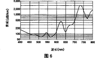
As mentioned above, be suppressed among a small circle by wavelength variation scope with laser 9 in, can effectively use the low-loss region of PMMA plastic optical fiber shown in Figure 6, can realize all the time in low-loss stable transfer characteristic., can carry out the distance of high speed, high capacity optical communication and can be extended significantly according to this transmitting device at this.
Again, thermoregulation mechanism, owing to just in-45~35 ℃ ambient temperature range, the temperature of semiconductor laser 5 is controlled at desired value, and in 35~85 ℃ ambient temperature range, do not carry out adjustment, therefore can less expensively form.Like this, the transmitting device of the present embodiment can be avoided increasing condition of cost significantly owing to carry out adjustment.
In addition, the semiconductor laser 5 of end face light emitting-type obtains the above height output of 3mW easily, can also higher output, by improving output, can the loss of the loss of the various joint portions that comprise fiber optics system be compensated, and because action stability at high temperature is good, carry out adjustment by heating, even operating temperature also can operating stably when higher,, be particularly suitable in the present invention using from these 2.
For example, when making the semiconductor laser of oscillation wavelength 645 ± 5nm (35 ℃), if as above-mentioned embodiment, actuating range is limited in 35~85 ℃ the scope, even consider the situation that characteristic is disperseed and component temperature changes of element, also oscillation wavelength can be limited in the scope of 640nm~660nm.For this reason, when adopting the PMMA plastic optical fiber of loss characteristic shown in Figure 6, can effectively utilize the following low-loss region of about 200dB/km.Specifically, adopt the PMMA plastic optical fiber of gradation type, can carry out the high speed of 1GHz, 100m, long Distance Transmission.
In addition, though adopt the type of focusing of globe lens 6 in the above-described embodiment, as focusing on also adopting globe lens lens in addition.Again, condenser lens also can be made in the window portion of jar shell body 2 in advance.Further the core diameter of plastic optical fiber is not limited to 700 μ m, 900 μ m that also can be outside this etc.Employed in the present invention plastic optical fiber is because core diameter is bigger, by in this optical fiber end of semiconductor light-emitting elements neighbor configuration, also can not use lens and laser is directly combined with optical fiber.
Again, thermoregulator desired value is higher than normal temperature by setting for, can effectively prevent the dewfall of each optical parameter.
Further, though adopt the end face emitting laser diode in the above-described embodiment, in the present invention also can the applicable surface emitting laser.In surface-emitting laser, the temperature dependency of oscillation wavelength, because the effect of DBR (Distributed Bragg Reflector) catoptron, it generally is about 1/3 of end face emitting laser diode, smaller, even do not carry out adjustment, also can allow oscillation wavelength mobility scale with above-mentioned embodiment in the same scope.But in order effectively to use low-loss especially zone of PMMA plastic optical fiber shown in Figure 6, preferred serviceability temperature is regulated and is limited in the narrower scope, from this viewpoint, can say in the present invention also can preferably be suitable for this surface-emitting laser.Also can be suitable for RC (Resonant Cavity)-LED of the LED that adopts the DBR catoptron equally, in the present invention.
Another embodiment of the present invention below is described.Fig. 2 represents to adopt the side view according to the transmitting device of the plastic optical fiber of the present invention's the 2nd embodiment, and again, Fig. 3 and Fig. 4 represent the flat shape and the front shape of the part on the counter-base frame of this transmitting device respectively.The transmitting device of the present embodiment, be the device that constitutes the transmission submodule 10 of signal transmitting and receiving module 30 shown in Figure 5 described later, comprise end face emitting laser diode 11, PMMA plastic optical fiber 12, fix counter-base frame 13 that the Si of these parts makes, fix this Si counter-base frame 13 and double as is the substrate 14 of heat sink.
Semiconductor laser chip 11, be oscillation wavelength 650nm under 25 ℃ of temperature, output 3mW, the temperature dependency of oscillation wavelength is about the device of 0.2nm/deg, by scolding tin weld its composition surface, promptly near the face of active layer 15 1 sides, be fixed on the Si counter-base frame 13.PMMA plastic optical fiber 12, the diameter of its fibre core 12a is 500 μ m, and the diameter that comprises covering is 700 μ m, and laser 16 direct irradiations that allow semiconductor laser chip 11 send are configured on the end face of this fibre core 12a like that.Like this, laser 16 incides in the fibre core 12a, transmits in the multimode mode.
On Si counter-base frame 13, contiguous semiconductor laser chip 11, fixing thermal resistor 17 as temperature-detecting device.Again, on Si counter-base frame 13, the separating tank 18 that allows semiconductor laser chip 11 separate with PMMA plastic optical fiber 12 is set, the groove 19 that the cross section that PMMA plastic optical fiber 12 is positioned is the V font is set simultaneously.PMMA plastic optical fiber 12 is positioned by above-mentioned V groove 19, by UV constrictive type adhesive securement on Si counter-base frame 13.
The subtended angle of the laser 16 that penetrates from semiconductor laser chip 11, its half value full-shape is about 30 degree, if the width of above-mentioned separating tank 18 about 50~100 μ m, even do not use lens, also can allow laser 16 combine with PMMA plastic optical fiber 12 with the efficient more than 70%.Again, by on semiconductor laser chip 11 and Si counter-base frame 13, telltale mark 20 being set, can allow the V groove 19 that PMMA plastic optical fiber 12 is positioned and the luminous position of semiconductor laser chip 11 aim at, just can realize hi-Fix by easy assembling.
In the present embodiment, same with the situation of the 1st embodiment, the temperature of semiconductor laser chip 11, by by the electric heater 22 in the interior plant substrate 14, as the thermal resistor 17 of temperature-detecting device, the thermoregulation mechanism that temperature-control circuit 12 constitutes, be set at desired value as heating arrangement.That is, temperature-control circuit 21 according to the drive current of the temperature detection signal S control electric heater 22 of thermal resistor 17 output, is that the temperature of semiconductor laser chip 11 remains on desired value with the temperature of substrate 14 thus.
In addition, the desired value of said temperature adjusting is set value lower than the maximum temperature that prefers in environment for use for.At this, environment temperature is for example also supposed the value that can get between-45~85 ℃, and then thermoregulator desired value is set 35 ℃ for.As the design temperature condition of regulating, the temperature of semiconductor laser chip 11 is controlled to 35 ℃ when the scope of environment temperature at-45~35 ℃, in surpassing 35 ℃ to 85 ℃ ambient temperature range, directly change with environment temperature.
But if the range of temperature of the semiconductor laser chip 11 when not carrying out adjustment is 130 ℃, by carrying out this adjustment, range of temperature can reduce by 50 ℃ significantly.For this reason, the mobility scale of the oscillation wavelength of semiconductor laser chip 11 can be suppressed to the degree of having only 10nm from about 26nm.Specifically, this oscillation wavelength is controlled at about 652nm when environment temperature is-45~35 ℃ scope, then, change in the scope at about 652nm~662nm when 35~85 ℃ scope.
As mentioned above, be suppressed among a small circle by wavelength variation scope with laser 16 in, can effectively use the low-loss region of PMMA plastic optical fiber shown in Figure 6, can realize all the time in low-loss stable transfer characteristic., in the present embodiment, can carry out the distance of high speed, high capacity optical communication and also can be extended significantly at this.
In addition, in the present embodiment,,, can more efficiently heat if on semiconductor laser chip 11, form well heater though the heating of semiconductor laser chip 11 is undertaken by the well heater of other setting.During the well heater of employing and semiconductor laser chip 11 other settings, also can not be arranged in the substrate 14, and be arranged on Si counter-base frame 13 grades again.
More than the signal of explanation sends submodule 10, is configured in the signal transmitting and receiving module 30 shown in Figure 5, and the PMMA plastic optical fiber 12 (not drawing among Fig. 5) of this submodule 10 adopts connector 31 to be connected with PMMA plastic optical fiber 32 with transmission.Again, each signal transmitting and receiving module 30 is connected with said temperature control circuit 21, is connected with signal transmitting and receiving circuit 33 simultaneously.
In this embodiment, in can the signal transmitting and receiving module 30 of two-way communication, send the signal that configuration receives with formations such as photodiodes outside the submodule 10 at signal and receive with submodule 40, this signal receives with submodule 40 and also adopts connector 31 to be connected with PMMA plastic optical fiber 32 with transmission.That is, in this example, 2 signal transmitting and receiving modules 30 connect by 2 optical fiber of connector 31 usefulness 32, constitute bidirectional optical telecommunication system.
In the above in Shuo Ming the embodiment, though configuration and transmission are with the identical optical fiber 12 of PMMA plastic optical fiber 32 in module, and combine with semiconductor light-emitting elements, the present invention effectively utilizes the low loss characteristic of the PMMA plastic optical fiber of transmission usefulness, obtain high performance transmitting device, therefore in module, might not need to adopt and the identical optical fiber that transmits usefulness, also can adopt by the optical fiber of glass, the optical system that can constitute with the suitable lens that combine of external fiber, optical waveguide etc.
In the above-described embodiment,,, have sometimes heating arrangement and the better situation of temperature-detecting device meeting are set outside submodule according to the device that adopts submodule though in submodule, be provided with heating arrangement and temperature-detecting device again.Further, for shared, perhaps, also heating arrangement and temperature-detecting device can be set externally in order simultaneously a plurality of submodules to be carried out temperature control with other purposes.
Again, in the present invention, be not limited to just form the plastic optical fiber of fibre core by PMMA, also can adopt the plastic optical fiber that forms fibre core by the material behind other material of interpolation in PMMA, at this moment the loss characteristic of plastic optical fiber, even loss value itself changes, have the formation of curve shown in Figure 6 in essence, can obtain identical effect with above explanation.Again, in the present invention, the material outside PMMA forms in the plastic optical fiber of fibre core, if having loss characteristic shown in Figure 6 in essence, and can be suitable equally.
Further, the transmitting device according to employing plastic optical fiber of the present invention is not limited to general optical communication, can utilize light signal to transmit in all systems of information.As the system beyond such optical communication, for example can enumerate digital developing and printing system.Fig. 7 represents that the summary of digital developing and printing system 310 constitutes, and Fig. 8 represents the outside drawing of digital developing and printing system 310.As shown in Figure 7, this laboratory system 310, constituted by line CCD scanner 314, image processing part 316, laser photo print apparatus portion 318 and handling part 320, line CCD scanner 314 and image processing part 316 are arranged in the input part 326 shown in Figure 8, and laser photo print apparatus portion 318 and handling part 320 are arranged in the efferent 328 shown in Figure 8.
Line CCD scanner 314 is used to read in the film image that writes down on the photographic films such as negative film or anti-sheet, can be for example so-called APS film), the film image of the photographic film of 120 sizes and 220 sizes (Brownie size) is as reading object with the photographic film of the photographic film of 135 sizes, 110 sizes and the formed photographic film of the transparent magnetic layer (photographic film of 240 sizes:.Line CCD scanner 314 employing line CCD read the film image of above-mentioned reading object, output image data.In addition, the face CCD scanner that the face CCD of utilization reads film image can be set also, substitute above-mentioned line CCD scanner 314.
Image processing part 316, the view data (scan image data) that incoming line CCD scanner 314 is exported, also can import simultaneously from the outside (for example by the input of storage mediums such as storage card or by communication line from other information processing apparatus inputs etc.) view data that obtains by the digital camera photography, with scanner read view data that original copy beyond the film image (for example reflextion copy etc.) obtained, the view data that generates by computing machine etc. (following these are referred to as document image data).
316 pairs of view data of being imported of image processing part are carried out the Flame Image Process of various corrections etc., as record with view data to 318 outputs of laser photo print apparatus portion.Again, image processing part 316 also can with the view data after the Flame Image Process as image document to outside output (for example to the output of storage mediums such as storage card or by communication line to other information processing apparatus outputs etc.).
Laser photo print apparatus portion 318 comprises the LASER Light Source of the laser that sends R, G, B color, will be according to the laser radiation after modulating with view data from the record of image processing part 316 inputs on photo papers, by scan exposure document image on photo papers.Again, handling part 320 to having write down the photo papers of image in laser photo print apparatus portion 318 by scan exposure, is implemented color development development, blix, washing, dry each and is handled.Like this, on photo papers, form image.
(formation of line CCD scanner)
Below the formation of line CCD scanner 314 is described.Fig. 9 represents that the summary of the optical system of line CCD scanner 314 constitutes.This optical system comprise constitute by halogen lamp or metal halide lamp lamp, be radiated at the light source 330 on the photographic film 322, at the light emitting side of light source 330, configuration allows and is radiated at the light diffusion chamber 336 that light on the photographic film 322 becomes diffusion light.
Photographic film 322 is transported on the direction vertical with optical axis by the film hanger rack 338 (referring to Figure 11, not drawing in Fig. 9) of the light emitting side that is configured in light diffusion chamber 336.In addition, though what illustrate in Fig. 9 is the photographic film 322 of long chi shape, for the filstrip (anti-sheet) and the APS film that each width of cloth are positioned on the magic lantern horse, by preparing each special-purpose film hanger rack (film hanger rack that APS uses comprises the magnetic head that reads in the information that writes down in the magnetosphere), also can transport these photographic films.
Again, between light source 330 and light diffusion chamber 336, set gradually C (green grass or young crops) respectively along the optical axis that penetrates light, M (magenta), light modulation optical filter 114C, 114M, the 114Y of Y (Huang) look, on clamping photographic film 322 and light source 330 opposite sides, dispose lens unit 340, the line CCD116 that allows through the photoimaging of film image successively along optical axis.In Fig. 9, though only show single lens as lens unit 340, lens unit 340 is actually the zoom lens that are made of the multi-disc lens.
Line CCD116, the a plurality of row that are configured to of the components of photo-electric conversion with CCD unit formation, and be provided with the induction part of electronic shutter mechanism, 3 lines that are arranged in parallel separated by a certain interval are installed the color separation filter (so-called 3 line colored CCDs) of R, G, B respectively on the light incident side of each induction part.Line CCD116 is configured to allow the sensitive surface of each induction part consistent with the image space of lens unit 340.Again, near each induction part, the corresponding transport unit that is provided with respectively with each induction part, the electric charge of savings on each CCD unit of each induction part, the transport unit by correspondence transmits successively.Though do not draw among the figure, between online CCD116 and the lens unit 340 shutter is set again.
Figure 10 represents that the summary of the electric system of line CCD scanner 314 constitutes.Line CCD scanner 314 comprises the microprocessor 46 that carries out the 314 whole controls of line CCD scanner.On microprocessor 46, connect RAM64 (for example SRAM), ROM66 (for example can rewrite the ROM of recorded content), connect motor driver 48 simultaneously, on motor driver 48, connect optical filter drive motor 54 by bus.Optical filter drive motor 54 can allow light modulation optical filter 114C, 114M, 114Y independently move separately.
Microprocessor 46, with the ON/OFF interlock of unillustrated power switch among the figure, allow light source 330 points, go out.Again, microprocessor 46, undertaken by line CCD116 film image read (photometry) time, allow light modulation optical filter 114C, 114M, 114Y independently move separately by optical filter drive motor 54, the light quantity that incides among the line CCD116 is regulated according to each composition color.
Again, on motor driver 48, connect by allow the position of multi-disc lens of lens unit 340 relatively move change lens unit 340 zoom ratio zoom drive motor 70 and by allowing the whole lens drive motor 106 that allows the image space of lens unit 340 move that moves of lens unit 340 along optical axis.Microprocessor 46 according to the size of film image with whether cut out etc., is altered to desirable multiplying power with zoom drive motor 70 with the zoom ratio of lens unit 340.
On the other hand, online CCD116 connects timing sequencer 74.Timing sequencer 74 produces the various clock signals (clock signal) that allow line CCD116 and A/D converter described later 82 etc. move.The signal output part of line CCD116 is connected with A/D converter 82 by amplifier 76, from the signal of line CCD116 output, after amplifier 76 amplifications, is transformed into numerical data by A/D converter 82.
The output terminal of A/D converter 82 is connected with interface (I/F) circuit 90 by correlated double sample circuit (CDS) 88.In CDS88, respectively the pixel data of the level of the feedthrough data of level of expression feed-through signal and remarked pixel signal is sampled, from pixel data, deduct the feedthrough data for each pixel.Then, with operation result (with the correct corresponding pixel data of the quantity of electric charge of putting aside in each CCD unit), export to image processing part 316 successively as scan image data by I/F circuit 90.
In addition, owing to export R, G, B photometry signal side by side from line CCD116, therefore, the signal Processing system that amplifier 76, A/D converter 82, CDS88 constitute also is provided with 3, and from I/F circuit 90, output is as R, G, the B view data of scan image data side by side.
On motor driver 48, connect the shutter drive motor 92 that allows shutter open and close again.For the dark output of line CCD116, to proofread and correct at the image processing part 316 of back segment, the level of dark output not carrying out film image when reading, can obtain shutter close by microprocessor 46.
(formation of image processing part)
The following formation that image processing part 316 is described with reference to Figure 11.Image processing part 316 is with the line CCD scanner 314 corresponding line sweep correction units 122 that are provided with.Line sweep correction unit 122 with corresponding from R, G, the B view data of 314 outputs in parallel of line CCD scanner, is provided with the signal Processing system that 3 systems are made of dark correction circuit 124, defect pixel correction portion 128 and bright correcting circuit 130.
Dark correction circuit 124, under the state of the light incident side of online CCD116 by the shutter shading, preserve by each unit from the data (data of the dark output level of each unit of the induction part of expression line CCD116) of line CCD scanner 314 inputs, by from the scan image data of line CCD scanner 314 inputs, deducting the dark output level of the unit corresponding, proofread and correct with each pixel.
Again, also can there be the dispersion of concentration in the light-to-signal transfer characteristic of line CCD116 in each unit of cells.In the bright correcting circuit 130 of defect pixel correction portion 128 back segments, the correction that integral image is had same concentration is provided with state in the online CCD scanner 314 with film image under, by read the film image of above-mentioned correction usefulness by line CCD116, according to (dispersion of each pixel concentration of expression of this view data is that the dispersion owing to the luminous point variation characteristic of each unit causes with the view data of film image from the correction of line CCD scanner 314 input, determine the gain of each unit, to view data from the film image of the reading object of line CCD scanner 314 input, according to the gain that each unit is determined, each pixel is proofreaied and correct.
On the other hand, proofreading and correct with in the view data of film image, when the concentration of other pixels of concentration ratio of specific pixel had very big-difference, the unit corresponding with above-mentioned specific pixel of line CCD116 occurred that certain is unusual, can judge that above-mentioned specific pixel is a defect pixel.Defect pixel correction portion 128 is according to the view data of proofreading and correct with film image, preserve the address of defect pixel, from the view data of the film image of the reading object of line CCD scanner 314 input, carry out interpolation for the data of the The data surrounding pixel of defect pixel, produce data again.
Again, line CCD116 is because upwardly extending 3 lines (CCD cell columns) dispose successively along the carriage direction of the photographic film 322 given interval that is separated by in the side vertical with the carriage direction of photographic film 322, from line CCD scanner 314 begin to export R, G, each composition color of B view data the time to be carved with certain hour poor.In line sweep correction unit 122, be provided with unillustrated delay circuit among the figure, for R, G, the B view data of the same pixel on film image can be exported simultaneously, with moment of view data of output at the latest as benchmark, adopt the different output times that carry out view data time delay to postpone to all the other 2 colors.
The output terminal of line sweep correction unit 122 is connected with the input end of selector switch 132, and the view data of correction unit 122 outputs inputs to selector switch 132.Again, the input end of selector switch also is connected with the data output end of input/output control unit 134, and the document image data of the outside being imported from input/output control unit 134 inputs to selector switch 132.The output terminal of selector switch 132 is connected with the data input pin of input/output control unit 134, image processing part 136A, 136B respectively.Selector switch 132 selects to export to input/output control unit 134, image processing part 136A, 136B respectively with the view data of being imported.
Image processing part 136A comprises Memory Controller 138, image processor 140,3 frame memory 142A, 142B, 142C.Frame memory 142A, 142B, 142C have the capacity of the view data of the film image that can store 1 frame amount respectively, from the view data of selector switch 132 input is kept at some 3 the frame memory 142, Memory Controller 138, each pixel data of the view data of importing in order to allow is kept at according to a definite sequence in the storage area of frame memory 142, and the address when view data being kept in the frame memory 142 is controlled.
Image processor 140, the view data of reading and saving in frame memory 142, the hypercolour of carry out greyscale transformation, tone reversal, the gray scale of the ultralow frequency briliancy composition of image being compressed is mediated reason, is suppressed the granular various Flame Image Process such as super sharpness processing of emphasizing sharpness.In addition, the treatment conditions of above-mentioned Flame Image Process are carried out computing automatically by engine 144 (aftermentioned) is set automatically, carry out Flame Image Process according to the treatment conditions of institute's computing.Image processor 140 is connected with input/output control unit 134, and the view data after the Flame Image Process is kept in the frame memory 142 earlier temporarily, exports to input/output control unit 134 according to the given moment then.In addition, image processing part 136B has identical formation with above-mentioned image processing part 136A, omits its explanation at this.
Line CCD scanner 314 also can read for 2 times with different resolution.Read (hereinafter referred to as prescan) with lower resolution the 1st time, even for example, carry out reading of film image not allow line CCD116 put aside the saturated reading conditions of electric charge (the electric charge savings time of R, the G of the light of irradiation photographic film, the light quantity of each wavelength region may of B, CCD) in the concentration (for example negative image of the overexposure in the negative film) under extremely low situation of film image.By the view data (pre-scan images data) that this prescan obtains, to input/output control unit 134 inputs, further export to the engine 144 that is provided with automatically that is connected with input/output control unit 134 from selector switch 132.
Engine 144 is set automatically comprises CPU146, RAM148 (for example DRAM), ROM50 (for example can rewrite the ROM of recorded content), input/output port 152, these interconnect by bus 154.
Engine 144 is set automatically, pre-scan images data according to several film images of importing from input/output control unit 134, determine by the 2nd light quantity that reads light source 330 in (hereinafter referred to as close scanning) of line CCD scanner 314 to carry out than higher resolution, the treatment conditions of the view data computing Flame Image Process that close scanning is obtained simultaneously are with image processor 140 outputs to image processing part 136 of the treatment conditions of computing.In the computing of the treatment conditions of this Flame Image Process, exposure, photography kind or further feature amount during according to photography are judged several the film images whether similar scene of having photographed is arranged, when if several film images of the similar scene of having photographed are arranged, the close scanning view data of these film images is determined to adopt the treatment conditions of identical or approximate Flame Image Process.
In addition, the optimization process of Flame Image Process is regulated, and is to be used for carrying out record images in laser photo print apparatus portion 318 on photographic paper according to the view data after the Flame Image Process, still changes to some extent to the difference of outside output etc.Image processing part 316 is owing to be provided with 2 image processing part 136A, 136B, for example simultaneously view data is being carried out record images and during to outside output etc. on the photo papers, engine 144 is set automatically respectively according to each purposes computing optimal treatment condition, exports to image processing part 136A, 136B.Like this, in image processing part 136A, 136B,, can carry out Flame Image Process with mutual different treatment conditions for same close scanning view data.
Further, the pre-scan images data of engine 144 according to the film image of importing from line CCD scanner 314 are set automatically, calculating is to the laser photo print apparatus portion 318 image recording parameter that gray balance during document image etc. is stipulated on photo papers, exporting simultaneously during with view data (aftermentioned) to 318 output records of laser photo print apparatus portion.Again, engine 144 is set automatically, for document image data from outside input, also treatment conditions of handling with above-mentioned same computed image.
Input/output control unit 134 is connected with laser photo print apparatus portion 318 by I/F circuit 156.When the view data after the Flame Image Process is used for carrying out record images on photo papers, carry out the view data of Flame Image Process by image processing part 136, from input/output control unit 134 by I/F circuit 156 as record with view data to 318 outputs of laser photo print apparatus portion.Again, engine 144 being set automatically is connected with microcomputer 158.View data after the Flame Image Process when export the outside, is carried out the view data of Flame Image Process by image processing part 136 as image document, from input/output control unit 134 by engine 144 being set automatically to microcomputer 158 outputs.
Microcomputer 158 comprises CPU160, storer 162, display 164 and keyboard 166 (also referring to Fig. 8), hard disk 168, CD-ROM drive 170, s operation control portion 172, expansion slot 174, image dwindle/enlarging section 176, and these interconnect by bus 178.Transport control part 172, be connected with film hanger rack 338, control film hanger rack 338 transports photographic film 322.Again, on film hanger rack 338, be provided be the APS film time, the information that film hanger rack 338 inputs are read from the magnetosphere of APS film (for example image recording size etc.).
Again, the communication control unit to recording mediums such as storage card carry out the driver of reading/writing (not drawing among the figure) of data, communicate with the out of Memory handling machine is connected with microcomputer 158 by expansion slot 174.When the view data of usefulness was exported in the outside, above-mentioned view data was exported to outside (above-mentioned driver or communication control unit etc.) as image document by expansion slot 174 from input/output control unit 134 inputs.Again, when importing document image data by expansion slot 174 from the outside, the document image data of input is by being provided with engine 144 automatically to input/output control unit 134 outputs.At this moment, be input to the view data of input/output control unit 134 to selector switch 132 outputs.
In addition, image processing part 316, pre-scan images data etc. are exported to microcomputer, to on display 164, show by the film image that line CCD scanner 314 reads, image and demonstration on display 164 that supposition obtains at record on the photo papers, if the operator has indicated correction to image etc. by keyboard 166, these also can be at the processing bar of Flame Image Process with middle reflection.
Figure 12 represents that the summary of the electric system of laser photo print apparatus portion 318 and handling part 320 constitutes.Laser photo print apparatus portion 318 comprises the frame memory 230 of recording image data.Frame memory 230 is connected with image processing part 316 by I/F circuit 232,, be kept in the frame memory 230 with view data (should in R, the G of each pixel of expression of photo papers 224 records, the view data of B concentration) from the record of image processing part 316 input by I/F circuit 232 temporarily.Frame memory 230 is connected with exposure portion 236 by D/A converter 234, is connected with photo print apparatus control circuit 238 simultaneously.
On arbitrary position that the information of carrying out transmits in above-mentioned digital developing and printing system, all be fit to suitable device of the present invention.Particularly, device of the present invention, transmitting (between the amplifier 76-A/D converter 82 of Figure 10, between the A/D converter 82-CDS88 from line CCD scanner to the data of image processing part, between the CDS88-I/F circuit 90), transmit (between the A/D converter 82-exposure portion 236 of Figure 12 from image processing part to the data of laser photo print apparatus portion, between the frame memory 230-A/D converter 234), transmit (between the input/output port 152-bus 178 of Figure 11) from image processing part to the data of master controller (microcomputer), transmit (between the graphics processing part 316-of Fig. 7 " recording medium or out of Memory handling machine etc. ") from master controller (microcomputer) to the data of external device (ED), can preferably be used for transmitting light signal the data transmission (the image processing part 316-laser photo print apparatus portion 318 of Figure 11) from reader to the output machine etc.
Further, device of the present invention also can be adapted at being suitable for the transmission of the information between each operation of input-editor (DTP)-output in the plate making technology.Again, the device of the present invention information that also can be adapted at medical field transmits in (for example the LAN hospital in, the LAN between the hospital, more specifically say information transmission between the terminal of the central server of the case record of having stored the patient and medical diagnostic images and each clinic etc.) suitable.