CN1303228A - Luminescence display apparatus and its manufacturing method - Google Patents
Luminescence display apparatus and its manufacturing method Download PDFInfo
- Publication number
- CN1303228A CN1303228A CN00136448A CN00136448A CN1303228A CN 1303228 A CN1303228 A CN 1303228A CN 00136448 A CN00136448 A CN 00136448A CN 00136448 A CN00136448 A CN 00136448A CN 1303228 A CN1303228 A CN 1303228A
- Authority
- CN
- China
- Prior art keywords
- equipment
- luminescent
- electrode
- luminescent material
- luminescent device
- Prior art date
- Legal status (The legal status is an assumption and is not a legal conclusion. Google has not performed a legal analysis and makes no representation as to the accuracy of the status listed.)
- Pending
Links
- 238000004519 manufacturing process Methods 0.000 title description 3
- 238000004020 luminiscence type Methods 0.000 title 1
- 239000000463 material Substances 0.000 claims abstract description 102
- 238000000034 method Methods 0.000 claims abstract description 21
- 238000007639 printing Methods 0.000 claims abstract description 10
- OAICVXFJPJFONN-UHFFFAOYSA-N Phosphorus Chemical compound [P] OAICVXFJPJFONN-UHFFFAOYSA-N 0.000 claims abstract description 7
- 239000000758 substrate Substances 0.000 claims description 23
- 239000000843 powder Substances 0.000 claims description 16
- 239000000853 adhesive Substances 0.000 claims description 8
- 230000001070 adhesive effect Effects 0.000 claims description 8
- 239000000975 dye Substances 0.000 claims description 6
- 230000015572 biosynthetic process Effects 0.000 claims description 3
- 230000001680 brushing effect Effects 0.000 claims description 2
- 239000006193 liquid solution Substances 0.000 claims 2
- 239000010410 layer Substances 0.000 description 63
- 229920000642 polymer Polymers 0.000 description 51
- 230000005525 hole transport Effects 0.000 description 20
- 239000000243 solution Substances 0.000 description 17
- 125000003983 fluorenyl group Chemical class C1(=CC=CC=2C3=CC=CC=C3CC12)* 0.000 description 16
- -1 polyparaphenylene Polymers 0.000 description 16
- 239000000203 mixture Substances 0.000 description 11
- 125000003118 aryl group Chemical group 0.000 description 9
- 229910052757 nitrogen Inorganic materials 0.000 description 9
- 229910052782 aluminium Inorganic materials 0.000 description 8
- 238000002347 injection Methods 0.000 description 8
- 239000007924 injection Substances 0.000 description 8
- 229920000548 poly(silane) polymer Polymers 0.000 description 8
- XAGFODPZIPBFFR-UHFFFAOYSA-N aluminium Chemical compound [Al] XAGFODPZIPBFFR-UHFFFAOYSA-N 0.000 description 7
- 150000001875 compounds Chemical class 0.000 description 7
- 239000011521 glass Substances 0.000 description 7
- 125000000843 phenylene group Chemical group C1(=C(C=CC=C1)*)* 0.000 description 7
- OKKJLVBELUTLKV-UHFFFAOYSA-N Methanol Chemical compound OC OKKJLVBELUTLKV-UHFFFAOYSA-N 0.000 description 6
- 239000004411 aluminium Substances 0.000 description 6
- 229910052799 carbon Inorganic materials 0.000 description 6
- 229910052751 metal Inorganic materials 0.000 description 6
- 239000002184 metal Substances 0.000 description 6
- QVGXLLKOCUKJST-UHFFFAOYSA-N atomic oxygen Chemical compound [O] QVGXLLKOCUKJST-UHFFFAOYSA-N 0.000 description 5
- 230000005540 biological transmission Effects 0.000 description 5
- 239000002019 doping agent Substances 0.000 description 5
- 238000005516 engineering process Methods 0.000 description 5
- 229910052736 halogen Inorganic materials 0.000 description 5
- MRNHPUHPBOKKQT-UHFFFAOYSA-N indium;tin;hydrate Chemical compound O.[In].[Sn] MRNHPUHPBOKKQT-UHFFFAOYSA-N 0.000 description 5
- 239000012120 mounting media Substances 0.000 description 5
- 229910052760 oxygen Inorganic materials 0.000 description 5
- 239000001301 oxygen Substances 0.000 description 5
- 229920003227 poly(N-vinyl carbazole) Polymers 0.000 description 5
- 229920003229 poly(methyl methacrylate) Polymers 0.000 description 5
- 239000004926 polymethyl methacrylate Substances 0.000 description 5
- IJGRMHOSHXDMSA-UHFFFAOYSA-N Atomic nitrogen Chemical compound N#N IJGRMHOSHXDMSA-UHFFFAOYSA-N 0.000 description 4
- PQMOXTJVIYEOQL-UHFFFAOYSA-N Cumarin Natural products CC(C)=CCC1=C(O)C(C(=O)C(C)CC)=C(O)C2=C1OC(=O)C=C2CCC PQMOXTJVIYEOQL-UHFFFAOYSA-N 0.000 description 4
- FSOGIJPGPZWNGO-UHFFFAOYSA-N Meomammein Natural products CCC(C)C(=O)C1=C(O)C(CC=C(C)C)=C(O)C2=C1OC(=O)C=C2CCC FSOGIJPGPZWNGO-UHFFFAOYSA-N 0.000 description 4
- 125000000217 alkyl group Chemical group 0.000 description 4
- 150000001721 carbon Chemical group 0.000 description 4
- 239000002800 charge carrier Substances 0.000 description 4
- ZYGHJZDHTFUPRJ-UHFFFAOYSA-N coumarin Chemical compound C1=CC=C2OC(=O)C=CC2=C1 ZYGHJZDHTFUPRJ-UHFFFAOYSA-N 0.000 description 4
- 230000006870 function Effects 0.000 description 4
- PQXKHYXIUOZZFA-UHFFFAOYSA-M lithium fluoride Chemical compound [Li+].[F-] PQXKHYXIUOZZFA-UHFFFAOYSA-M 0.000 description 4
- 239000002609 medium Substances 0.000 description 4
- NIHNNTQXNPWCJQ-UHFFFAOYSA-N o-biphenylenemethane Natural products C1=CC=C2CC3=CC=CC=C3C2=C1 NIHNNTQXNPWCJQ-UHFFFAOYSA-N 0.000 description 4
- 238000012545 processing Methods 0.000 description 4
- VYPSYNLAJGMNEJ-UHFFFAOYSA-N silicon dioxide Inorganic materials O=[Si]=O VYPSYNLAJGMNEJ-UHFFFAOYSA-N 0.000 description 4
- 238000004528 spin coating Methods 0.000 description 4
- VEUMBMHMMCOFAG-UHFFFAOYSA-N 2,3-dihydrooxadiazole Chemical compound N1NC=CO1 VEUMBMHMMCOFAG-UHFFFAOYSA-N 0.000 description 3
- 229920002799 BoPET Polymers 0.000 description 3
- 239000005041 Mylar™ Substances 0.000 description 3
- 229920001609 Poly(3,4-ethylenedioxythiophene) Polymers 0.000 description 3
- BQCADISMDOOEFD-UHFFFAOYSA-N Silver Chemical compound [Ag] BQCADISMDOOEFD-UHFFFAOYSA-N 0.000 description 3
- YXFVVABEGXRONW-UHFFFAOYSA-N Toluene Chemical compound CC1=CC=CC=C1 YXFVVABEGXRONW-UHFFFAOYSA-N 0.000 description 3
- 150000001412 amines Chemical class 0.000 description 3
- 239000012298 atmosphere Substances 0.000 description 3
- 239000013522 chelant Substances 0.000 description 3
- 125000004122 cyclic group Chemical group 0.000 description 3
- 239000002270 dispersing agent Substances 0.000 description 3
- PCHJSUWPFVWCPO-UHFFFAOYSA-N gold Chemical compound [Au] PCHJSUWPFVWCPO-UHFFFAOYSA-N 0.000 description 3
- 229910052737 gold Inorganic materials 0.000 description 3
- 239000010931 gold Substances 0.000 description 3
- 150000002367 halogens Chemical class 0.000 description 3
- 239000011777 magnesium Substances 0.000 description 3
- 238000002156 mixing Methods 0.000 description 3
- 230000006798 recombination Effects 0.000 description 3
- 238000005215 recombination Methods 0.000 description 3
- 235000012239 silicon dioxide Nutrition 0.000 description 3
- 229910052709 silver Inorganic materials 0.000 description 3
- 239000004332 silver Substances 0.000 description 3
- 239000002904 solvent Substances 0.000 description 3
- SCYULBFZEHDVBN-UHFFFAOYSA-N 1,1-Dichloroethane Chemical compound CC(Cl)Cl SCYULBFZEHDVBN-UHFFFAOYSA-N 0.000 description 2
- YMMGRPLNZPTZBS-UHFFFAOYSA-N 2,3-dihydrothieno[2,3-b][1,4]dioxine Chemical compound O1CCOC2=C1C=CS2 YMMGRPLNZPTZBS-UHFFFAOYSA-N 0.000 description 2
- OYPRJOBELJOOCE-UHFFFAOYSA-N Calcium Chemical compound [Ca] OYPRJOBELJOOCE-UHFFFAOYSA-N 0.000 description 2
- 241000252203 Clupea harengus Species 0.000 description 2
- LFQSCWFLJHTTHZ-UHFFFAOYSA-N Ethanol Chemical compound CCO LFQSCWFLJHTTHZ-UHFFFAOYSA-N 0.000 description 2
- 239000001856 Ethyl cellulose Substances 0.000 description 2
- ZZSNKZQZMQGXPY-UHFFFAOYSA-N Ethyl cellulose Chemical compound CCOCC1OC(OC)C(OCC)C(OCC)C1OC1C(O)C(O)C(OC)C(CO)O1 ZZSNKZQZMQGXPY-UHFFFAOYSA-N 0.000 description 2
- UFHFLCQGNIYNRP-UHFFFAOYSA-N Hydrogen Chemical compound [H][H] UFHFLCQGNIYNRP-UHFFFAOYSA-N 0.000 description 2
- KFZMGEQAYNKOFK-UHFFFAOYSA-N Isopropanol Chemical compound CC(C)O KFZMGEQAYNKOFK-UHFFFAOYSA-N 0.000 description 2
- FYYHWMGAXLPEAU-UHFFFAOYSA-N Magnesium Chemical compound [Mg] FYYHWMGAXLPEAU-UHFFFAOYSA-N 0.000 description 2
- LRHPLDYGYMQRHN-UHFFFAOYSA-N N-Butanol Chemical class CCCCO LRHPLDYGYMQRHN-UHFFFAOYSA-N 0.000 description 2
- PXHVJJICTQNCMI-UHFFFAOYSA-N Nickel Chemical compound [Ni] PXHVJJICTQNCMI-UHFFFAOYSA-N 0.000 description 2
- 241000233855 Orchidaceae Species 0.000 description 2
- NINIDFKCEFEMDL-UHFFFAOYSA-N Sulfur Chemical compound [S] NINIDFKCEFEMDL-UHFFFAOYSA-N 0.000 description 2
- 239000005864 Sulphur Substances 0.000 description 2
- ATJFFYVFTNAWJD-UHFFFAOYSA-N Tin Chemical compound [Sn] ATJFFYVFTNAWJD-UHFFFAOYSA-N 0.000 description 2
- MCMNRKCIXSYSNV-UHFFFAOYSA-N Zirconium dioxide Chemical compound O=[Zr]=O MCMNRKCIXSYSNV-UHFFFAOYSA-N 0.000 description 2
- 239000002253 acid Substances 0.000 description 2
- 125000003545 alkoxy group Chemical group 0.000 description 2
- MWPLVEDNUUSJAV-UHFFFAOYSA-N anthracene Chemical compound C1=CC=CC2=CC3=CC=CC=C3C=C21 MWPLVEDNUUSJAV-UHFFFAOYSA-N 0.000 description 2
- 230000004888 barrier function Effects 0.000 description 2
- 230000008901 benefit Effects 0.000 description 2
- 229910052791 calcium Inorganic materials 0.000 description 2
- 239000011575 calcium Substances 0.000 description 2
- 239000011248 coating agent Substances 0.000 description 2
- 238000000576 coating method Methods 0.000 description 2
- 238000007796 conventional method Methods 0.000 description 2
- 239000006184 cosolvent Substances 0.000 description 2
- 238000013461 design Methods 0.000 description 2
- 230000006866 deterioration Effects 0.000 description 2
- 238000010586 diagram Methods 0.000 description 2
- 239000003989 dielectric material Substances 0.000 description 2
- 238000003618 dip coating Methods 0.000 description 2
- 230000005684 electric field Effects 0.000 description 2
- 238000005401 electroluminescence Methods 0.000 description 2
- 239000003822 epoxy resin Substances 0.000 description 2
- 150000002148 esters Chemical class 0.000 description 2
- 229920001249 ethyl cellulose Polymers 0.000 description 2
- 235000019325 ethyl cellulose Nutrition 0.000 description 2
- 150000002240 furans Chemical class 0.000 description 2
- 238000010438 heat treatment Methods 0.000 description 2
- 235000019514 herring Nutrition 0.000 description 2
- 125000001183 hydrocarbyl group Chemical group 0.000 description 2
- 229910052739 hydrogen Inorganic materials 0.000 description 2
- 239000001257 hydrogen Substances 0.000 description 2
- 238000005286 illumination Methods 0.000 description 2
- 229910052738 indium Inorganic materials 0.000 description 2
- APFVFJFRJDLVQX-UHFFFAOYSA-N indium atom Chemical compound [In] APFVFJFRJDLVQX-UHFFFAOYSA-N 0.000 description 2
- 239000003446 ligand Substances 0.000 description 2
- 239000007788 liquid Substances 0.000 description 2
- 230000004807 localization Effects 0.000 description 2
- 229910052749 magnesium Inorganic materials 0.000 description 2
- 125000004433 nitrogen atom Chemical group N* 0.000 description 2
- 239000003921 oil Substances 0.000 description 2
- 239000003960 organic solvent Substances 0.000 description 2
- 230000003647 oxidation Effects 0.000 description 2
- 238000007254 oxidation reaction Methods 0.000 description 2
- 239000002245 particle Substances 0.000 description 2
- 238000005424 photoluminescence Methods 0.000 description 2
- IEQIEDJGQAUEQZ-UHFFFAOYSA-N phthalocyanine Chemical compound N1C(N=C2C3=CC=CC=C3C(N=C3C4=CC=CC=C4C(=N4)N3)=N2)=C(C=CC=C2)C2=C1N=C1C2=CC=CC=C2C4=N1 IEQIEDJGQAUEQZ-UHFFFAOYSA-N 0.000 description 2
- 229920000647 polyepoxide Polymers 0.000 description 2
- 238000002360 preparation method Methods 0.000 description 2
- 239000010453 quartz Substances 0.000 description 2
- MCJGNVYPOGVAJF-UHFFFAOYSA-N quinolin-8-ol Chemical compound C1=CN=C2C(O)=CC=CC2=C1 MCJGNVYPOGVAJF-UHFFFAOYSA-N 0.000 description 2
- LIVNPJMFVYWSIS-UHFFFAOYSA-N silicon monoxide Chemical compound [Si-]#[O+] LIVNPJMFVYWSIS-UHFFFAOYSA-N 0.000 description 2
- 238000001228 spectrum Methods 0.000 description 2
- 125000001424 substituent group Chemical group 0.000 description 2
- 239000011135 tin Substances 0.000 description 2
- 229910052718 tin Inorganic materials 0.000 description 2
- 238000012546 transfer Methods 0.000 description 2
- 125000005389 trialkylsiloxy group Chemical group 0.000 description 2
- XLYOFNOQVPJJNP-UHFFFAOYSA-N water Substances O XLYOFNOQVPJJNP-UHFFFAOYSA-N 0.000 description 2
- DXWHZJXKTHGHQF-UHFFFAOYSA-N 2-butyl-6-(butylamino)benzo[de]isoquinoline-1,3-dione Chemical compound O=C1N(CCCC)C(=O)C2=CC=CC3=C2C1=CC=C3NCCCC DXWHZJXKTHGHQF-UHFFFAOYSA-N 0.000 description 1
- DNTVTBIKSZRANH-UHFFFAOYSA-N 4-(4-aminophenyl)-3-(3-methylphenyl)aniline Chemical class CC1=CC=CC(C=2C(=CC=C(N)C=2)C=2C=CC(N)=CC=2)=C1 DNTVTBIKSZRANH-UHFFFAOYSA-N 0.000 description 1
- XLPKAUDSAPXLJO-UHFFFAOYSA-N 4-bromo-2-[[2-[(5-bromo-2-hydroxyphenyl)methylideneamino]phenyl]iminomethyl]phenol Chemical compound OC1=CC=C(Br)C=C1C=NC1=CC=CC=C1N=CC1=CC(Br)=CC=C1O XLPKAUDSAPXLJO-UHFFFAOYSA-N 0.000 description 1
- PLXMOAALOJOTIY-FPTXNFDTSA-N Aesculin Natural products OC[C@@H]1[C@@H](O)[C@H](O)[C@@H](O)[C@H](O)[C@H]1Oc2cc3C=CC(=O)Oc3cc2O PLXMOAALOJOTIY-FPTXNFDTSA-N 0.000 description 1
- 229910001316 Ag alloy Inorganic materials 0.000 description 1
- SZVKJTDZEOTYCX-UHFFFAOYSA-N CN(C1=CC(=C(C=C1)CC1=CC=CC=C1)CN)C Chemical compound CN(C1=CC(=C(C=C1)CC1=CC=CC=C1)CN)C SZVKJTDZEOTYCX-UHFFFAOYSA-N 0.000 description 1
- 101100189588 Canis lupus familiaris PDE6B gene Proteins 0.000 description 1
- OKTJSMMVPCPJKN-UHFFFAOYSA-N Carbon Chemical compound [C] OKTJSMMVPCPJKN-UHFFFAOYSA-N 0.000 description 1
- VGGSQFUCUMXWEO-UHFFFAOYSA-N Ethene Chemical compound C=C VGGSQFUCUMXWEO-UHFFFAOYSA-N 0.000 description 1
- PXGOKWXKJXAPGV-UHFFFAOYSA-N Fluorine Chemical compound FF PXGOKWXKJXAPGV-UHFFFAOYSA-N 0.000 description 1
- 229910000861 Mg alloy Inorganic materials 0.000 description 1
- CBENFWSGALASAD-UHFFFAOYSA-N Ozone Chemical compound [O-][O+]=O CBENFWSGALASAD-UHFFFAOYSA-N 0.000 description 1
- XYFCBTPGUUZFHI-UHFFFAOYSA-N Phosphine Chemical compound P XYFCBTPGUUZFHI-UHFFFAOYSA-N 0.000 description 1
- 239000004698 Polyethylene Substances 0.000 description 1
- 229920000265 Polyparaphenylene Polymers 0.000 description 1
- 239000004743 Polypropylene Substances 0.000 description 1
- 239000004793 Polystyrene Substances 0.000 description 1
- 229910052581 Si3N4 Inorganic materials 0.000 description 1
- BLRPTPMANUNPDV-UHFFFAOYSA-N Silane Chemical compound [SiH4] BLRPTPMANUNPDV-UHFFFAOYSA-N 0.000 description 1
- XUIMIQQOPSSXEZ-UHFFFAOYSA-N Silicon Chemical compound [Si] XUIMIQQOPSSXEZ-UHFFFAOYSA-N 0.000 description 1
- 239000004809 Teflon Substances 0.000 description 1
- 229920006362 Teflon® Polymers 0.000 description 1
- RTAQQCXQSZGOHL-UHFFFAOYSA-N Titanium Chemical compound [Ti] RTAQQCXQSZGOHL-UHFFFAOYSA-N 0.000 description 1
- HCHKCACWOHOZIP-UHFFFAOYSA-N Zinc Chemical compound [Zn] HCHKCACWOHOZIP-UHFFFAOYSA-N 0.000 description 1
- 230000002745 absorbent Effects 0.000 description 1
- 239000002250 absorbent Substances 0.000 description 1
- 230000009102 absorption Effects 0.000 description 1
- 238000010521 absorption reaction Methods 0.000 description 1
- 239000012190 activator Substances 0.000 description 1
- 239000003831 antifriction material Substances 0.000 description 1
- 150000004982 aromatic amines Chemical class 0.000 description 1
- 125000004429 atom Chemical group 0.000 description 1
- 239000011230 binding agent Substances 0.000 description 1
- 235000010290 biphenyl Nutrition 0.000 description 1
- 239000004305 biphenyl Substances 0.000 description 1
- 238000009835 boiling Methods 0.000 description 1
- 239000007767 bonding agent Substances 0.000 description 1
- XZCJVWCMJYNSQO-UHFFFAOYSA-N butyl pbd Chemical compound C1=CC(C(C)(C)C)=CC=C1C1=NN=C(C=2C=CC(=CC=2)C=2C=CC=CC=2)O1 XZCJVWCMJYNSQO-UHFFFAOYSA-N 0.000 description 1
- 239000000969 carrier Substances 0.000 description 1
- 230000003197 catalytic effect Effects 0.000 description 1
- 230000008859 change Effects 0.000 description 1
- 239000003795 chemical substances by application Substances 0.000 description 1
- 125000001309 chloro group Chemical group Cl* 0.000 description 1
- 239000003086 colorant Substances 0.000 description 1
- 150000004696 coordination complex Chemical class 0.000 description 1
- 230000007797 corrosion Effects 0.000 description 1
- 238000005260 corrosion Methods 0.000 description 1
- VBVAVBCYMYWNOU-UHFFFAOYSA-N coumarin 6 Chemical compound C1=CC=C2SC(C3=CC4=CC=C(C=C4OC3=O)N(CC)CC)=NC2=C1 VBVAVBCYMYWNOU-UHFFFAOYSA-N 0.000 description 1
- 125000000113 cyclohexyl group Chemical class [H]C1([H])C([H])([H])C([H])([H])C([H])(*)C([H])([H])C1([H])[H] 0.000 description 1
- 238000000354 decomposition reaction Methods 0.000 description 1
- 238000009792 diffusion process Methods 0.000 description 1
- 238000001035 drying Methods 0.000 description 1
- 238000005538 encapsulation Methods 0.000 description 1
- ZOOODBUHSVUZEM-UHFFFAOYSA-N ethoxymethanedithioic acid Chemical compound CCOC(S)=S ZOOODBUHSVUZEM-UHFFFAOYSA-N 0.000 description 1
- 238000001704 evaporation Methods 0.000 description 1
- 230000008020 evaporation Effects 0.000 description 1
- 230000005281 excited state Effects 0.000 description 1
- 229910052731 fluorine Inorganic materials 0.000 description 1
- 239000011737 fluorine Substances 0.000 description 1
- 239000002223 garnet Substances 0.000 description 1
- YBMRDBCBODYGJE-UHFFFAOYSA-N germanium oxide Inorganic materials O=[Ge]=O YBMRDBCBODYGJE-UHFFFAOYSA-N 0.000 description 1
- 238000000227 grinding Methods 0.000 description 1
- 230000005283 ground state Effects 0.000 description 1
- 125000000623 heterocyclic group Chemical group 0.000 description 1
- XMBWDFGMSWQBCA-UHFFFAOYSA-N hydrogen iodide Chemical compound I XMBWDFGMSWQBCA-UHFFFAOYSA-N 0.000 description 1
- 230000007062 hydrolysis Effects 0.000 description 1
- 238000006460 hydrolysis reaction Methods 0.000 description 1
- 229920001600 hydrophobic polymer Polymers 0.000 description 1
- 229910010272 inorganic material Inorganic materials 0.000 description 1
- 239000011147 inorganic material Substances 0.000 description 1
- 239000011810 insulating material Substances 0.000 description 1
- 238000009413 insulation Methods 0.000 description 1
- 150000002576 ketones Chemical class 0.000 description 1
- 239000011133 lead Substances 0.000 description 1
- 229960004194 lidocaine Drugs 0.000 description 1
- 229910052744 lithium Inorganic materials 0.000 description 1
- WPBNNNQJVZRUHP-UHFFFAOYSA-L manganese(2+);methyl n-[[2-(methoxycarbonylcarbamothioylamino)phenyl]carbamothioyl]carbamate;n-[2-(sulfidocarbothioylamino)ethyl]carbamodithioate Chemical compound [Mn+2].[S-]C(=S)NCCNC([S-])=S.COC(=O)NC(=S)NC1=CC=CC=C1NC(=S)NC(=O)OC WPBNNNQJVZRUHP-UHFFFAOYSA-L 0.000 description 1
- 238000012986 modification Methods 0.000 description 1
- 230000004048 modification Effects 0.000 description 1
- KKFHAJHLJHVUDM-UHFFFAOYSA-N n-vinylcarbazole Chemical compound C1=CC=C2N(C=C)C3=CC=CC=C3C2=C1 KKFHAJHLJHVUDM-UHFFFAOYSA-N 0.000 description 1
- 125000001624 naphthyl group Chemical group 0.000 description 1
- 150000002815 nickel Chemical class 0.000 description 1
- 229910052759 nickel Inorganic materials 0.000 description 1
- VOFUROIFQGPCGE-UHFFFAOYSA-N nile red Chemical compound C1=CC=C2C3=NC4=CC=C(N(CC)CC)C=C4OC3=CC(=O)C2=C1 VOFUROIFQGPCGE-UHFFFAOYSA-N 0.000 description 1
- NICDRCVJGXLKSF-UHFFFAOYSA-N nitric acid;trihydrochloride Chemical compound Cl.Cl.Cl.O[N+]([O-])=O NICDRCVJGXLKSF-UHFFFAOYSA-N 0.000 description 1
- 125000000449 nitro group Chemical group [O-][N+](*)=O 0.000 description 1
- 239000006250 one-dimensional material Substances 0.000 description 1
- 239000011368 organic material Substances 0.000 description 1
- PVADDRMAFCOOPC-UHFFFAOYSA-N oxogermanium Chemical compound [Ge]=O PVADDRMAFCOOPC-UHFFFAOYSA-N 0.000 description 1
- 229960003540 oxyquinoline Drugs 0.000 description 1
- 238000004806 packaging method and process Methods 0.000 description 1
- 238000012856 packing Methods 0.000 description 1
- 125000001997 phenyl group Chemical group [H]C1=C([H])C([H])=C(*)C([H])=C1[H] 0.000 description 1
- ZUOUZKKEUPVFJK-UHFFFAOYSA-N phenylbenzene Natural products C1=CC=CC=C1C1=CC=CC=C1 ZUOUZKKEUPVFJK-UHFFFAOYSA-N 0.000 description 1
- 229910052698 phosphorus Inorganic materials 0.000 description 1
- 239000011574 phosphorus Substances 0.000 description 1
- 229920003023 plastic Polymers 0.000 description 1
- 239000004033 plastic Substances 0.000 description 1
- 230000010287 polarization Effects 0.000 description 1
- 229920003201 poly(di-n-hexylsilylene) polymer Polymers 0.000 description 1
- 229920000573 polyethylene Polymers 0.000 description 1
- 229920006254 polymer film Polymers 0.000 description 1
- 229920000098 polyolefin Polymers 0.000 description 1
- 229920001155 polypropylene Polymers 0.000 description 1
- 229920001296 polysiloxane Polymers 0.000 description 1
- 229920002223 polystyrene Polymers 0.000 description 1
- 230000008569 process Effects 0.000 description 1
- 230000005855 radiation Effects 0.000 description 1
- 238000007761 roller coating Methods 0.000 description 1
- 238000007650 screen-printing Methods 0.000 description 1
- 238000000926 separation method Methods 0.000 description 1
- 229910000077 silane Inorganic materials 0.000 description 1
- 239000010703 silicon Substances 0.000 description 1
- 229910052710 silicon Inorganic materials 0.000 description 1
- 239000000377 silicon dioxide Substances 0.000 description 1
- HQVNEWCFYHHQES-UHFFFAOYSA-N silicon nitride Chemical compound N12[Si]34N5[Si]62N3[Si]51N64 HQVNEWCFYHHQES-UHFFFAOYSA-N 0.000 description 1
- 239000002356 single layer Substances 0.000 description 1
- 239000007787 solid Substances 0.000 description 1
- 239000006104 solid solution Substances 0.000 description 1
- 230000003595 spectral effect Effects 0.000 description 1
- 238000005507 spraying Methods 0.000 description 1
- 230000007480 spreading Effects 0.000 description 1
- 238000003892 spreading Methods 0.000 description 1
- 230000006641 stabilisation Effects 0.000 description 1
- 239000000126 substance Substances 0.000 description 1
- 239000004094 surface-active agent Substances 0.000 description 1
- 239000000725 suspension Substances 0.000 description 1
- 238000003786 synthesis reaction Methods 0.000 description 1
- BFKJFAAPBSQJPD-UHFFFAOYSA-N tetrafluoroethene Chemical compound FC(F)=C(F)F BFKJFAAPBSQJPD-UHFFFAOYSA-N 0.000 description 1
- 238000009210 therapy by ultrasound Methods 0.000 description 1
- 229920001187 thermosetting polymer Polymers 0.000 description 1
- XOLBLPGZBRYERU-UHFFFAOYSA-N tin dioxide Chemical compound O=[Sn]=O XOLBLPGZBRYERU-UHFFFAOYSA-N 0.000 description 1
- 229910001887 tin oxide Inorganic materials 0.000 description 1
- 229910052719 titanium Inorganic materials 0.000 description 1
- 239000010936 titanium Substances 0.000 description 1
- 125000003944 tolyl group Chemical group 0.000 description 1
- 238000001771 vacuum deposition Methods 0.000 description 1
- 238000007740 vapor deposition Methods 0.000 description 1
- 238000005406 washing Methods 0.000 description 1
- 239000012991 xanthate Substances 0.000 description 1
- 229910052725 zinc Inorganic materials 0.000 description 1
- 239000011701 zinc Substances 0.000 description 1
Images


Classifications
-
- H—ELECTRICITY
- H01—ELECTRIC ELEMENTS
- H01L—SEMICONDUCTOR DEVICES NOT COVERED BY CLASS H10
- H01L31/00—Semiconductor devices sensitive to infrared radiation, light, electromagnetic radiation of shorter wavelength or corpuscular radiation and specially adapted either for the conversion of the energy of such radiation into electrical energy or for the control of electrical energy by such radiation; Processes or apparatus specially adapted for the manufacture or treatment thereof or of parts thereof; Details thereof
- H01L31/12—Semiconductor devices sensitive to infrared radiation, light, electromagnetic radiation of shorter wavelength or corpuscular radiation and specially adapted either for the conversion of the energy of such radiation into electrical energy or for the control of electrical energy by such radiation; Processes or apparatus specially adapted for the manufacture or treatment thereof or of parts thereof; Details thereof structurally associated with, e.g. formed in or on a common substrate with, one or more electric light sources, e.g. electroluminescent light sources, and electrically or optically coupled thereto
-
- C—CHEMISTRY; METALLURGY
- C09—DYES; PAINTS; POLISHES; NATURAL RESINS; ADHESIVES; COMPOSITIONS NOT OTHERWISE PROVIDED FOR; APPLICATIONS OF MATERIALS NOT OTHERWISE PROVIDED FOR
- C09D—COATING COMPOSITIONS, e.g. PAINTS, VARNISHES OR LACQUERS; FILLING PASTES; CHEMICAL PAINT OR INK REMOVERS; INKS; CORRECTING FLUIDS; WOODSTAINS; PASTES OR SOLIDS FOR COLOURING OR PRINTING; USE OF MATERIALS THEREFOR
- C09D11/00—Inks
- C09D11/30—Inkjet printing inks
- C09D11/32—Inkjet printing inks characterised by colouring agents
- C09D11/328—Inkjet printing inks characterised by colouring agents characterised by dyes
-
- G—PHYSICS
- G09—EDUCATION; CRYPTOGRAPHY; DISPLAY; ADVERTISING; SEALS
- G09F—DISPLAYING; ADVERTISING; SIGNS; LABELS OR NAME-PLATES; SEALS
- G09F13/00—Illuminated signs; Luminous advertising
- G09F13/20—Illuminated signs; Luminous advertising with luminescent surfaces or parts
- G09F13/22—Illuminated signs; Luminous advertising with luminescent surfaces or parts electroluminescent
-
- H—ELECTRICITY
- H05—ELECTRIC TECHNIQUES NOT OTHERWISE PROVIDED FOR
- H05B—ELECTRIC HEATING; ELECTRIC LIGHT SOURCES NOT OTHERWISE PROVIDED FOR; CIRCUIT ARRANGEMENTS FOR ELECTRIC LIGHT SOURCES, IN GENERAL
- H05B33/00—Electroluminescent light sources
- H05B33/02—Details
-
- H—ELECTRICITY
- H05—ELECTRIC TECHNIQUES NOT OTHERWISE PROVIDED FOR
- H05B—ELECTRIC HEATING; ELECTRIC LIGHT SOURCES NOT OTHERWISE PROVIDED FOR; CIRCUIT ARRANGEMENTS FOR ELECTRIC LIGHT SOURCES, IN GENERAL
- H05B33/00—Electroluminescent light sources
- H05B33/12—Light sources with substantially two-dimensional radiating surfaces
- H05B33/14—Light sources with substantially two-dimensional radiating surfaces characterised by the chemical or physical composition or the arrangement of the electroluminescent material, or by the simultaneous addition of the electroluminescent material in or onto the light source
-
- H—ELECTRICITY
- H05—ELECTRIC TECHNIQUES NOT OTHERWISE PROVIDED FOR
- H05B—ELECTRIC HEATING; ELECTRIC LIGHT SOURCES NOT OTHERWISE PROVIDED FOR; CIRCUIT ARRANGEMENTS FOR ELECTRIC LIGHT SOURCES, IN GENERAL
- H05B33/00—Electroluminescent light sources
- H05B33/12—Light sources with substantially two-dimensional radiating surfaces
- H05B33/22—Light sources with substantially two-dimensional radiating surfaces characterised by the chemical or physical composition or the arrangement of auxiliary dielectric or reflective layers
-
- H—ELECTRICITY
- H10—SEMICONDUCTOR DEVICES; ELECTRIC SOLID-STATE DEVICES NOT OTHERWISE PROVIDED FOR
- H10K—ORGANIC ELECTRIC SOLID-STATE DEVICES
- H10K50/00—Organic light-emitting devices
- H10K50/80—Constructional details
- H10K50/805—Electrodes
-
- H—ELECTRICITY
- H10—SEMICONDUCTOR DEVICES; ELECTRIC SOLID-STATE DEVICES NOT OTHERWISE PROVIDED FOR
- H10K—ORGANIC ELECTRIC SOLID-STATE DEVICES
- H10K59/00—Integrated devices, or assemblies of multiple devices, comprising at least one organic light-emitting element covered by group H10K50/00
- H10K59/10—OLED displays
- H10K59/221—Static displays, e.g. displaying permanent logos
-
- H—ELECTRICITY
- H10—SEMICONDUCTOR DEVICES; ELECTRIC SOLID-STATE DEVICES NOT OTHERWISE PROVIDED FOR
- H10K—ORGANIC ELECTRIC SOLID-STATE DEVICES
- H10K59/00—Integrated devices, or assemblies of multiple devices, comprising at least one organic light-emitting element covered by group H10K50/00
- H10K59/30—Devices specially adapted for multicolour light emission
- H10K59/35—Devices specially adapted for multicolour light emission comprising red-green-blue [RGB] subpixels
-
- H—ELECTRICITY
- H10—SEMICONDUCTOR DEVICES; ELECTRIC SOLID-STATE DEVICES NOT OTHERWISE PROVIDED FOR
- H10K—ORGANIC ELECTRIC SOLID-STATE DEVICES
- H10K59/00—Integrated devices, or assemblies of multiple devices, comprising at least one organic light-emitting element covered by group H10K50/00
- H10K59/30—Devices specially adapted for multicolour light emission
- H10K59/38—Devices specially adapted for multicolour light emission comprising colour filters or colour changing media [CCM]
-
- H—ELECTRICITY
- H10—SEMICONDUCTOR DEVICES; ELECTRIC SOLID-STATE DEVICES NOT OTHERWISE PROVIDED FOR
- H10K—ORGANIC ELECTRIC SOLID-STATE DEVICES
- H10K59/00—Integrated devices, or assemblies of multiple devices, comprising at least one organic light-emitting element covered by group H10K50/00
- H10K59/80—Constructional details
- H10K59/86—Series electrical configurations of multiple OLEDs
-
- H—ELECTRICITY
- H10—SEMICONDUCTOR DEVICES; ELECTRIC SOLID-STATE DEVICES NOT OTHERWISE PROVIDED FOR
- H10K—ORGANIC ELECTRIC SOLID-STATE DEVICES
- H10K71/00—Manufacture or treatment specially adapted for the organic devices covered by this subclass
-
- H—ELECTRICITY
- H01—ELECTRIC ELEMENTS
- H01L—SEMICONDUCTOR DEVICES NOT COVERED BY CLASS H10
- H01L2221/00—Processes or apparatus adapted for the manufacture or treatment of semiconductor or solid state devices or of parts thereof covered by H01L21/00
- H01L2221/67—Apparatus for handling semiconductor or electric solid state devices during manufacture or treatment thereof; Apparatus for handling wafers during manufacture or treatment of semiconductor or electric solid state devices or components; Apparatus not specifically provided for elsewhere
- H01L2221/683—Apparatus for handling semiconductor or electric solid state devices during manufacture or treatment thereof; Apparatus for handling wafers during manufacture or treatment of semiconductor or electric solid state devices or components; Apparatus not specifically provided for elsewhere for supporting or gripping
- H01L2221/68304—Apparatus for handling semiconductor or electric solid state devices during manufacture or treatment thereof; Apparatus for handling wafers during manufacture or treatment of semiconductor or electric solid state devices or components; Apparatus not specifically provided for elsewhere for supporting or gripping using temporarily an auxiliary support
- H01L2221/68359—Apparatus for handling semiconductor or electric solid state devices during manufacture or treatment thereof; Apparatus for handling wafers during manufacture or treatment of semiconductor or electric solid state devices or components; Apparatus not specifically provided for elsewhere for supporting or gripping using temporarily an auxiliary support used as a support during manufacture of interconnect decals or build up layers
-
- H—ELECTRICITY
- H10—SEMICONDUCTOR DEVICES; ELECTRIC SOLID-STATE DEVICES NOT OTHERWISE PROVIDED FOR
- H10K—ORGANIC ELECTRIC SOLID-STATE DEVICES
- H10K50/00—Organic light-emitting devices
- H10K50/80—Constructional details
- H10K50/84—Passivation; Containers; Encapsulations
- H10K50/844—Encapsulations
-
- H—ELECTRICITY
- H10—SEMICONDUCTOR DEVICES; ELECTRIC SOLID-STATE DEVICES NOT OTHERWISE PROVIDED FOR
- H10K—ORGANIC ELECTRIC SOLID-STATE DEVICES
- H10K71/00—Manufacture or treatment specially adapted for the organic devices covered by this subclass
- H10K71/10—Deposition of organic active material
- H10K71/12—Deposition of organic active material using liquid deposition, e.g. spin coating
- H10K71/13—Deposition of organic active material using liquid deposition, e.g. spin coating using printing techniques, e.g. ink-jet printing or screen printing
- H10K71/135—Deposition of organic active material using liquid deposition, e.g. spin coating using printing techniques, e.g. ink-jet printing or screen printing using ink-jet printing
-
- H—ELECTRICITY
- H10—SEMICONDUCTOR DEVICES; ELECTRIC SOLID-STATE DEVICES NOT OTHERWISE PROVIDED FOR
- H10K—ORGANIC ELECTRIC SOLID-STATE DEVICES
- H10K71/00—Manufacture or treatment specially adapted for the organic devices covered by this subclass
- H10K71/841—Applying alternating current [AC] during manufacturing or treatment
-
- H—ELECTRICITY
- H10—SEMICONDUCTOR DEVICES; ELECTRIC SOLID-STATE DEVICES NOT OTHERWISE PROVIDED FOR
- H10K—ORGANIC ELECTRIC SOLID-STATE DEVICES
- H10K85/00—Organic materials used in the body or electrodes of devices covered by this subclass
- H10K85/10—Organic polymers or oligomers
- H10K85/111—Organic polymers or oligomers comprising aromatic, heteroaromatic, or aryl chains, e.g. polyaniline, polyphenylene or polyphenylene vinylene
- H10K85/113—Heteroaromatic compounds comprising sulfur or selene, e.g. polythiophene
- H10K85/1135—Polyethylene dioxythiophene [PEDOT]; Derivatives thereof
-
- H—ELECTRICITY
- H10—SEMICONDUCTOR DEVICES; ELECTRIC SOLID-STATE DEVICES NOT OTHERWISE PROVIDED FOR
- H10K—ORGANIC ELECTRIC SOLID-STATE DEVICES
- H10K85/00—Organic materials used in the body or electrodes of devices covered by this subclass
- H10K85/10—Organic polymers or oligomers
- H10K85/141—Organic polymers or oligomers comprising aliphatic or olefinic chains, e.g. poly N-vinylcarbazol, PVC or PTFE
- H10K85/146—Organic polymers or oligomers comprising aliphatic or olefinic chains, e.g. poly N-vinylcarbazol, PVC or PTFE poly N-vinylcarbazol; Derivatives thereof
-
- H—ELECTRICITY
- H10—SEMICONDUCTOR DEVICES; ELECTRIC SOLID-STATE DEVICES NOT OTHERWISE PROVIDED FOR
- H10K—ORGANIC ELECTRIC SOLID-STATE DEVICES
- H10K85/00—Organic materials used in the body or electrodes of devices covered by this subclass
- H10K85/30—Coordination compounds
- H10K85/321—Metal complexes comprising a group IIIA element, e.g. Tris (8-hydroxyquinoline) gallium [Gaq3]
- H10K85/324—Metal complexes comprising a group IIIA element, e.g. Tris (8-hydroxyquinoline) gallium [Gaq3] comprising aluminium, e.g. Alq3
-
- H—ELECTRICITY
- H10—SEMICONDUCTOR DEVICES; ELECTRIC SOLID-STATE DEVICES NOT OTHERWISE PROVIDED FOR
- H10K—ORGANIC ELECTRIC SOLID-STATE DEVICES
- H10K85/00—Organic materials used in the body or electrodes of devices covered by this subclass
- H10K85/60—Organic compounds having low molecular weight
- H10K85/631—Amine compounds having at least two aryl rest on at least one amine-nitrogen atom, e.g. triphenylamine
-
- H—ELECTRICITY
- H10—SEMICONDUCTOR DEVICES; ELECTRIC SOLID-STATE DEVICES NOT OTHERWISE PROVIDED FOR
- H10K—ORGANIC ELECTRIC SOLID-STATE DEVICES
- H10K85/00—Organic materials used in the body or electrodes of devices covered by this subclass
- H10K85/60—Organic compounds having low molecular weight
- H10K85/649—Aromatic compounds comprising a hetero atom
- H10K85/656—Aromatic compounds comprising a hetero atom comprising two or more different heteroatoms per ring
- H10K85/6565—Oxadiazole compounds
Abstract
The invention relates to a luminescent display comprising a first electrode, a second electrode, an organic light emitting layer disposed between the first and second electrodes, and a luminescent material which receives light from the organic light emitting layer and converts the light to a different wavelength, wherein the first and second electrodes together define an overlap region in which the organic light emitting layer is activated to emit light, and the luminescent material is disposed in a portion of the overlap region. The invention also relates to a method comprising the steps of creating an image and printing the image on a light emitting device comprising an organic light emitting layer after the light emitting device has been formed. The image may be created, for example on a personal computer, and printed with an inkjet printer. The image may be printed in phosphors which emit light of one wavelength upon absorbing light of a different wavelength from the organic light emitti Various embodiments of the invention allow customized luminescent displays to be easily fabricated by end users by applying a phosphor pattern to a preformed, encapsulated light emitting device.
Description
The present invention relates generally to the illumination application, particularly comprise the display device of luminous organic material.
All wish to make a kind of cheap mark that can see in the dark for a long time.Conventional measure is to utilize glass or the plastic plate that has one or more colour filters, and wherein one or more colour filters are arranged in and produce desirable mark when being placed on the back of the body end light.Such example is common " EXIT " mark.But this technology is not easy customization (customizable), because the terminal use can not easily design and produce this mark.Most of terminal use does not have the needed instrument of color filter plate itself of manufacturing or professional knowledge.Thereby the terminal use must obtain the service of color filter plate manufacturer to make the mark of customization.Most of terminal use does not do this trial.
A lot of technology have been developed to allow the mark of the easier customization that can read in the dark.Major part changes on the cathode ray tube (CRT) display in these technology.This display can be reset apace electronically to show new mark.Other technology with this ability comprises LCD, film plasma scope and display of organic electroluminescence.But these displays need very complicated electronic equipment and are too expensive for a lot of simple displaying tag application.
Thereby, need a kind of simple, cheap luminescent marking that can be customized at an easy rate by the terminal use for a long time.
The present invention relates to active display, this display comprises first electrode, second electrode, is arranged on organic luminous layer and luminescent material between first and second electrodes, this luminescent material receives light and converts light to different wave length from organic luminous layer, wherein first and second electrodes are determined an overlapping region together, organic luminous layer is excited luminously in this overlapping region, and luminescent material is arranged in a part of overlapping region.
The invention still further relates to the solution form fluorescent material, comprise the luminescent device of first electrode, second electrode and organic luminous layer and fluorescent material be applied to device on the luminescent device.This bringing device can comprise the ink-cases of printers that for example contains at least a fluorescent material.This ink-cases of printers can be used for printing luminescent material on luminescent device.This bringing device also can comprise hand-operated tools, as brushing, flat-rammer or pen.Fluorescent material solution can with any desirable figure and color by spreading, impress or write on the luminescent device.
The invention still further relates to a kind of method, this method may further comprise the steps: the generation image also prints images onto on the luminescent device that comprises organic luminous layer after forming luminescent device.This image can for example form on personal computer, and uses printing of inkjet printer.This image can be printed to according to the light of the different wave length that absorbs from organic luminous layer to be launched a kind of fluorescent material of light of wavelength.
Various embodiment of the present invention allows that the active display that is customized easily made by apply the fluorescent material figure on prefabricated, packaged light emitting device by the terminal use.This luminescent device is usually included in the organic luminous layer that illumination is provided on the high surface area.The fluorescent material figure can be applied on the luminescent device with the available a variety of modes of terminal use, as utilizes computer printer or hand-operated tools.Computer produces the utilizability of image and allows that the terminal use makes the active display of professional quality with minimum equipment investment.
Detailed description by following preferred embodiments and drawings makes other features and advantages of the present invention more obvious, wherein:
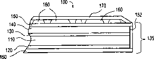
Fig. 1 is the profile of the active display of exemplary embodiments according to the present invention;
Fig. 2-the 5th, the profile of organic luminous layer according to other embodiments of the present invention;
Fig. 6 is the perspective view of the active display of exemplary embodiments according to the present invention;
Fig. 7 is used for luminescent material is applied to schematic representation of apparatus on the luminescent device according to an exemplary embodiment of the present invention;
Fig. 8 is used for luminescent material is applied to schematic representation of apparatus on the luminescent device according to another embodiment of the present invention;
Fig. 9 is a schematic diagram of representing the luminous zone of active display according to an exemplary embodiment of the present invention;
Figure 10 is the profile that according to another embodiment of the present invention luminescent material is applied to the device on the luminescent device;
Figure 11 is the schematic diagram that comprises the typical active display of a plurality of electrodes.
Referring to Fig. 1, wherein show the profile of active display according to an exemplary embodiment of the present invention.Fig. 6 represents the perspective view of active display.Active display 100 comprises that being arranged on two electrodes is organic luminous layer 110 between negative electrode 120 and the anode 130.Organic luminous layer 110 is luminous according to the voltage that is applied between anode and the negative electrode.Anode and negative electrode iunjected charge charge carrier in organic luminous layer 110 is hole and electronics, and they are compound to form excited molecule or exciton in organic luminous layer 110, and are luminous when this molecule or exciton decomposition.Color by the light of molecular emission depends on the excited state of molecule or exciton and the energy difference between the ground state.Usually, the voltage that applies is about 3-10 volt, but can be up to 30 volts or higher, and external quantum efficiency (photon output/electronics enters) is between 0.01% and 5% or higher.The thickness of organic luminous layer 110 generally is about 50-500nm, and the thickness of electrode 120,130 generally respectively is about 100-1000nm.
Various organic luminous layers 110 can be used in combination with exemplary embodiments of the present invention.According to an embodiment shown in Figure 1, organic luminous layer 110 comprises individual layer.Organic luminous layer 110 can comprise it for example being the luminous hole transport polymer of gripping polymer, usefulness electron transporting molecule and luminescent material doping altogether or the inert polymer that mixes with hole transport molecule and luminescent material.Organic luminous layer 110 also can comprise the amorphous film of the luminous little organic molecule that can mix with other light emitting molecule.
According to the other embodiments of the invention shown in Fig. 2-5, organic luminous layer 110 comprises two or more sublayers of realizing hole injection, hole transport, electronics injection, electric transmission and lighting function.Be used for operated device and only need luminescent layer.But hole and electron recombination generally can be improved to produce the efficient of light in additional sublayer.Therefore organic luminous layer 110 can comprise 1-4 sublayer, for example comprises that injection sublayer, hole, hole transport sublayer, luminous sublayer and electronics inject the sublayer.And one or more sublayers can comprise can realize as hole injection, hole transport, electronics injection, electric transmission and two or more materials with function such as luminous.
Introduce the embodiment that organic luminous layer 110 comprises individual layer below, as shown in Figure 1.
According to first embodiment, organic luminous layer 110 comprises grips polymer altogether.Term is gripped polymer altogether and is referred to along main polymer chain and comprise the not polymer of localization π-electron system.Localization π-electron system does not provide the semiconductive performance and supports to have the ability of high mobility positive and negative electric charge carrier along polymer chain to it to polymer.Polymer film has the extrinsic electric charge carrier of the enough low concentrations that apply electric field between electrode, and electric charge carrier is injected in the polymer and from the polymer emitted radiation.Grip polymer altogether for example at R.H.Friend, among the 4Journalof Molecular Electronics37-46 (1988) argumentation is arranged.
According to the luminous example gripping polymer altogether of the voltage that applies is PPV (the inferior ethene of polyparaphenylene).PPV is transmitted in the light in about 500-690nm spectral region and has good heat-resistant and resist the performance that causes the stress that breaks.The suitable common thickness of PPV film is about 100-1000nm.Can by spin coating guide on substrate in the methyl alcohol PPV solution and in vacuum furnace, add thermosetting PPV film.
Can make various modifications to PPV and keep its luminescent properties simultaneously.For example, the phenylene ring of PPV can randomly have one or more substituting groups, respectively is independently selected from alkyl, alkoxyl, halogen or nitro.Other that obtains from PPV gripped polymer altogether and also can be used in combination with exemplary embodiments of the present invention.The example of this PPV derivative comprises: the 1) polymer that replaces the phenylene ring to obtain with condensed ring system for example replaces the phenylene ring with anthracene or naphthalene ring system.These alternative ring systems can also have one or more substituting groups of the above-mentioned type with respect to the phenylene endless belt; 2) polymer that replaces the phenylene ring to obtain as furan nucleus with heterocycle system.Furan nucleus can have one or more substituting groups of the above-mentioned type with phenylene loops crossed belt; 3) by increasing and 1 of each phenylene or the association of other ring system, the polymer that the quantity of 2-ethenylidene part obtains.Said derivative has different energy gaps, has flexibility during this organic luminous layer 110 of launching in being created in a desirable color gamut or a plurality of scope.In United States Patent (USP) 5247190, description is arranged about luminous additional information of gripping polymer altogether, quote for reference here.
Suitable other example of gripping polymer altogether comprises poly-fluorenes, as 2, and fluorenes and 9-substituted fluorene oligomer and polymer that 7-replacement-9-replaces.Fluorenes, oligomer and polymer replace in the 9-position with two hydrocarbyl portions, and described hydrocarbyl portion can at random contain one or more in sulphur, nitrogen, oxygen, phosphorus or the sila atom; On the fluorenes ring, be formed with the C of 9-carbon
5-20Ring structure or contain the C of one or more the heteroatomic 9-of being formed with carbon of sulphur, nitrogen or oxygen
4-20Ring structure; Perhaps alkyl subunit part.According to an embodiment, fluorenes is replaced at 2-and 7-position by aryl moiety, and this aryl can be further with can part or trialkylsiloxy crosslinked or chain elongation partly replacing.Fluorenes polymer and oligomer can be substituted in 2-and 7 '-position.The monomeric unit of fluorenes oligomer and polymer is binding each other in 2-and 7 '-position.By making can be crosslinked or the end 2 of chain elongation, the arbitrary portion on 7 '-aryl moiety carries out chain elongation or crosslinked, and 2,7 '-aryl-9-substituted fluorene oligomer and further interreaction of polymer form higher molecular weight polymer.
At the catalytic amount that there is divalent nickel salt in the solvent in polarization promptly at least under the situation of the stoichiometric amount of zinc powder and trialkyl hydrogen phosphide, 2, under the condition that 7-aryl-9-substituted fluorene or 9-substituted fluorene oligomer or polymer are produced, by one or more 2,7-dihalo--9-substituted fluorene contacts with one or more halogen aromatic compounds, further with reactive group or trialkylsiloxy crosslinked or chain elongation partly replacing, prepare 2 thus, 7-dihalo-9-substituted fluorene or 9-substituted fluorene oligomer or polymer.Ending at the terminal 2-that has hydrogen or halogen and the 9-substituted fluorene low polymer and the polymer of 7 '-position is produced under the situation that does not have the halogen aromatic compounds by above-mentioned technology.
Fluorenes and fluorenes oligomer or polymer present the high light photoluminescence solid-state.When this material is exposed to wavelength about 300 light time to about 700nm, this material wavelength of light emitted arrives in the scope of about 800nm about 400.More preferably, the light of this absorbed wavelength in from the light of about wavelength of 350 to about 400nm and emission about 400 to about 650nm scope.Fluorenes of the present invention and fluorenes oligomer or polymer are easy to dissolve in ordinary organic solvents.Utilize as routine techniquess such as spin coating, spraying, dip-coating and roller coating, they can be processed into film or coating.When solidifying, this film presents the performance and the high-fire resistance of anti-ordinary organic solvents.Out of Memory about poly-fluorenes has introduction in United States Patent (USP) 5708130, quote as proof for reference here.
According to second embodiment of as shown in Figure 1 single layer device, organic luminous layer 110 comprises the molecular dopant polymer.The molecular dopant polymer is usually included in the binary solid solution of the charge transfer molecule of molecular diffusion in the inert polymer adhesive.This charge transfer molecule has improved the hole and electronics passes doped polymer and compound ability.Inert polymer provides a lot of alternatives with regard to the dopant material of available host polymer adhesive and mechanical performance.
An example of molecular dopant polymer comprises with hole transport molecule N, N '-hexichol-N, N '-two (3-methyl-phenyl)-1,1 '-biphenyl-4,4 '-diamines (TPD) and luminescent material three (oxine base)-aluminium (III) is the polymethyl methacrylate of molecular dopant (PMMA) (Alq).TDP has 10
-3Cm
2The high hole drift rate of/volt-sec, and Alq is the luminescent metal complexes that also has electronic transmission performance except its luminescent properties.
It is about 50% that doping content is generally, and the molar ratio of TDP and Alq is as changing from about 0.4 to 0.1.The film of DOPED PMMA can by mixing contain TPD, the Alq of appropriate amount and PMMA dichloroethane solution and with this solution dip-coating to the desirable substrate for example tin indium oxide (ITO) electrode prepare.The thickness of doping PMMA layer is generally about 100nm.When applying voltage-activated, produce green emission.About the out of Memory of this doped polymer " Organic Electroluminescent Devices Basedon Molecularly Doped Polymers " people such as Junji Kido, 61 Appl.Phys.Lett.761-763 have introduction in (1992), quote for reference here.
According to another embodiment of the present invention shown in Figure 2, organic luminous layer 110 comprises two sublayers.First sublayer 11 provide hole transport, electric transmission and luminescent properties and with negative electrode 120 adjacent settings.Second sublayer 12 be used as the hole inject the sublayer and with anode 130 adjacent settings.First sublayer 11 comprises with electron transporting molecule and luminescent material such as dyestuff or polymer-doped hole transport polymer.Hole transport polymer can comprise that for example poly-(N-vinylcarbazole) (PVK).Electron transporting molecule can comprise for example 2-(4-biphenyl)-5-(4-tert-butyl-phenyl)-1,3,4-oxadiazole (PBD).Luminescent material generally includes and is used as luminescence center to change the micromolecule or the polymer of emission color.For example, luminescent material can include organic dye cumarin 460 (orchid), coumarin 6 (green) or Nile red.Above-mentioned material is can obtain on market, for example from Aldrich Chemical Inc., and Lancaster Synthesis Inc., TCIAmerica, and Lambda Physik Inc. can obtain.Can form the film of these mixtures by the chloroformic solution that spin coating contains PVK, electron transporting molecule and the luminescent materials of different amounts.For example, suitable mixture comprises the PVK of 100 percentage by weights, the PBD of 40 percentage by weights and the organic dyestuff of 0.2-1.0 percentage by weight.
Example 1
The following formation of blue colour organic luminous device.The glass (15 ohm-square) that scribbles tin indium oxide (ITO) can be purchased from Applied Films Corportion, and uses the chloroazotic acid steam that its partial corrosion is fallen.This then substrate cleans with washing agent machinery, is immersed in the methanol solution, is immersed in then in the aqueous isopropanol of boiling, is placed at last in the ozone clean device 5 minutes.The layer that is similar to 5 nanometers (nm) that gathers (3,4) Ethylenedioxy Thiophene/polystyrene xanthate acid (PEDT/PSS) from Bayer Corportion is spun onto on the ITO then.Utilize then dichloroethanes do solvent will by from poly-(the 9-vinylcarbazole) of Aldrich company (PVK), from 2-(4-the biphenyl)-5-(4-tert-butyl benzene)-1 of Aldrich company, 3, the polymeric blends of 4-oxadiazole (PBD) and about 100nm of constituting with 100: 40: 1 percentage by weights from the 7-lignocaine-4-methylcoumarin (cumarin 460) of Exciton company is spun on the PEDT layer.Then, the negative electrode that is made of the aluminium of the lithium fluoride layer of about 0.8nm and about 100nm is evaporated on the device with definite cathode pattern by orifice plate.This device is transferred in the drying box then, and with epoxy resin glass slide is fixed to negative electrode one side of device so that encapsulation.The device that obtains is according to applying voltage emission blue streak.
According to another embodiment of the present invention shown in Figure 3, organic luminous layer 110 comprises first sublayer 13 that comprises luminous sublayer and second sublayer 14 that comprises the hole transport sublayer.Hole transport sublayer 14 can comprise at an easy rate and the aromatic amine of oxidation reversibly.For example, the hole transport compound can comprise at room temperature being that solid and at least one nitrogen-atoms are used the trisubstituted amine of substituting group, and wherein at least one is an aryl in the substituting group.Aryl substituent in the hole transport compound comprises aryl and unsubstituting aromatic yl, as phenyl and tolyl.Available substituent example comprises the alkoxyl of alkyl, halogen such as chloro, a fluorine and 1-5 carbon atom of 1 to 5 carbon atom, as methoxyl group, ethyoxyl and propoxyl group.Specific example comprises 1, two (4-two-right-tolyl aminophenyl) cyclohexanes of 1-; N, N, N-three (right-tolyl) amine; 1, two (4-two-right-tolyl the aminophenyl)-4-cyclohexylbenzenes of 1-; With 2 (4-dimethylamino-2-aminomethyl phenyl) phenylmethane.
The luminescent material example that is fit to that is used for luminous sublayer 13 comprises 4,4 '-two (5,7-two-uncle pentyl-2-benzoxazolyl)-Stilbene; 2, two (5,7-two-uncle pentyl-2-benzoxazolyl)-1,2 of 5-, 4-thiadiazoles; With the metal complex of 8 oxyquinolines, the metal here is Zn, Al, Mg or Li.Luminous sublayer 13 and hole transport sublayer 14 can utilize conventional vacuum deposition technique to form.Additional information about this device has introduction in United States Patent (USP) 4539507, quote as proof for reference here.
According to another embodiment of the present invention shown in Figure 4, organic luminous layer 110 includes first sublayer 15 of luminous and hole transport performance and second sublayer 16 of electronics injection efficiency is arranged.First sublayer 15 comprises polysilane, the second sublayer Bao Kuo oxadiazole compound.This structure will produce ultraviolet (UV) light.
Polysilane is linear silicon (the Si)-trunk polymer that replaces with various alkyl and/or aryl side family.Grip the polymer phase ratio altogether with π, polysilane is to have the accurate one-dimensional material that non-localized σ grips electronics altogether along main polymer chain.Because their the straight crack of one dimension (direct-gap) character, polysilane are presented on the strong photoluminescence performance that has high-quantum efficiency in the ultraviolet region.The example of suitable polysilane comprises poly-(two-just-butyl silane (PDBS)), poly-(two-n-pentyl silane) (PDPS), poly-(two-n-hexyl-silane) (PDHS), poly-(methyl-phenyl silane) (PMPS) and poly-[two (right-butyl phenyl) silane] (PBPS).For example can utilize the spin coating toluene solution to apply polysilane sublayer 15.Electric transmission sublayer 16 for example can comprise 2, two (the 4-biphenyl)-1,3 of 5-, 4-oxadiazole (BBD).About the out of Memory of the polysilane organic luminous layer of UV-emission " Near-ultraviolet Electroluminescence from Polysilanes " people such as Hiroyuki Suzuki, among the 331 ThinSolid Films 64-70 (1998) introduction is arranged, quote as proof for reference here.
According to another embodiment of the present invention shown in Figure 5, organic luminous layer 110 comprises that injection sublayer 17, hole, hole transport sublayer 18, luminous sublayer 19 and electronics inject sublayer 20.Sublayer 17 is injected in the hole and hole transport sublayer 18 offers recombination region with the hole effectively.Electronics injects sublayer 20 and effectively electronics is offered recombination region.
The above-mentioned example of organic luminous layer 110 can be used for designing the luminescent device of one or more desirable colors of emission.For example, luminescent device 135 can be launched one or more of ultraviolet, orchid, green and ruddiness.Can apply two or more organic luminous layers 110 by zones of different and form not homochromy district to identical electrodes with heterogeneity.Term " luminescent device " refers generally to the combination of organic luminous layer 110, negative electrode 120 and anode 130.As shown in Figure 1, luminescent device 135 also can comprise substrate 140.Substrate 140 provides substrate, can be on this substrate in forming process deposit anode 130, organic luminous layer 110 and negative electrode 120.Substrate can comprise for example glass or transparent polymer, as MYLAR.Luminescent device 135 and luminescent material 160 form active display 100 together.
According to another embodiment, encapsulated layer 150 or its part can comprise polymer, as the MYLAR with dielectric material such as silicon monoxide, silicon dioxide, silicon nitride, germanium oxide or zirconia coating.If necessary, can on dielectric material, apply one deck hydrophobic polymer, as polysiloxanes, TEFLON or branch branched polyolefin, for example polyethylene or polypropylene.According to this embodiment, encapsulated layer 150 also can be used as substrate 140, so that can omit the substrate 140 of separation.Other method for packing and material have introduction in United States Patent (USP) 5874804 and 5952778, quote as proof for reference here.
As shown in Figure 1, luminescent material 160 puts on luminescent device 135 surfaces.Luminescent material 160 absorbs the energy in a part of electromagnetic spectrum and launches energy in another part electromagnetic spectrum, with well known in the art the same.Usually, luminescent material 160 comprises inorganic fluorescent powder.A lot of inorganic fluorescent powders have generally to oxygen or the insensitive advantage of moisture.Thereby, they can be applied in encapsulated electroluminescent device 135 the outside and can be owing to long and remarkable deterioration of time.But, also can use luminescent material such as organic fluorescent material of other type.
The example of suitable red emission inorganic fluorescent powder is SrB
4O
7: Sm
2+, Sm wherein
2+Follow the color showing activator.Most of visible wavelength that this fluorescent material absorptance 600nm is short and emission are as the light that has greater than the dark red colo(u)r streak of 650nm wavelength.SrB
4O
7: Sm
2+Can be by mixing SrCO3,5% excessive H
3BO
3, Sm
2O
3, and with mixture under 900 ℃ under the reducing atmosphere for example in 5% hydrogen the heating 5 hours the preparation.Other suitable red-light fluorescent powder comprises by Sm
2+The SrB that activates
6O
10, BaMgF
4And LiBaF
3, BaFCl.
The example of suitable yellow emission inorganic fluorescent powder is Y
3Al
5O
12: Ce
3+This fluorescent material absorbs and is lower than most of wavelength of 500nm and has emission maximum at about 570-580nm.Can pass through Y
2O
3, Al
2O
3, CeO
2With the 3 molar percentage AlF that are used as cosolvent
3Mix and prepare Y
3Al
5O
12: Ce
3+Then this mixture was heated 6-8 hour down at 1500 ℃ in light reducing atmosphere.
The example of suitable green emission inorganic fluorescent powder is SrGa
2S
4: Eu
2+This fluorescent material absorbs and is lower than the wavelength of 500nm and has emission maximum in 535 nanometers.Can be by for example mixing Ga
2O
3, SrCO
3And Eu
2O
3And at 900 ℃ at H
2The down heating 4 hours of S air-flow, then under the same conditions 1000 ℃ of grindings and again processing prepare SrGa
2S
4: Eu
2+
The example of suitable blue streak emission inorganic fluorescent powder is BaMg
2Al
16O
27: Eu
2+BaMg
2Al
16O
27: Eu
2+Absorb the following most of wavelength of 430nm and have emission maximum at 450nm.BaMg
2Al
16O
27: Eu
2+Can pass through at 1400 ℃ of roasting BaCO in reducing atmosphere
3, MgO, Al
2O
3And Eu
2O
3Mixture prepare.
The example that can be used as the organic fluorescence materials of luminescent material 160 is 7-lignocaine-4-methylcoumarin (from cumarins 460 of Exciton company), and it absorbs and is lower than the wavelength of 420nm and launches blue streak; 3-(2 '-benzothiazolyl)-7-lignocaine cumarin (from the cumarin 540 of Exciton company), it absorbs following wavelength of 500nm and transmitting green light; 4-cyanogen methylene-2-methyl-6-(right-the dimethylamino styryl)-4H-pyrans (from the DCM of Exciton company), it absorbs following wavelength of 550nm and red-emitting; From the Fluorol 7GA of Exciton company, it absorbs and is lower than the wavelength of 500nm and launches gold-tinted; 3,3 '-diethyl oxa-carboxyl-anine iodide (from the DOCI of Exciton company), it absorbs following wavelength of 500nm and transmitting green light; Nile is red-and (Adrich company), its absorbs the following wavelength of 600nm and red-emitting.
Include under the organic dye situation at luminescent material 160, organic dyestuff can be dissolved in the mounting medium usually.This mounting medium can comprise for example water, if necessary, can also comprise water-soluble cosolvent, as ethanol, ketone or ester.Can also add the surface tension of surfactant, as known in the art with regulator solution.
Fig. 8 represents to be used for according to an exemplary embodiment of the present invention applying to luminescent device 135 device 200 of luminescent material 160.This device 200 comprises computer 210, printer 220, monitor 230 and keyboard 240.Computer 210 comprises memory 212, center processing unit 214, random access memory 216 and modulator-demodulator 218 in the middle of other parts.Memory 212 stores as information such as digital pictures.The such as known in the art processing instruction of center processing unit 214.Modulator-demodulator 218 provides the interface with computer network such as the Internet, and can receive digital picture from the Internet.Printer 220 receives data such as view data from computer 210, and according to the data print image.Printer 220 can comprise the print cartridge 222 that transmits at least a fluorescent material solution according to order to substrate such as luminescent device 135.Ink-cases of printers 222 can comprise for example three containers of fluorescent material solution, and is promptly red, green and blue, and they are printed on the substrate to produce coloured image.
Be not assembled in the standard printer or under the soft inadequately situation, image is printed on the intermediate substrate at luminescent device 135.For example, the fluorescent material figure is printed on 8.5 * 11 inches cellotone sheets with clear binder bottom.The printing intermediate substrate that has the fluorescent material figure then on it can bond on the luminescent device 135 by the adhesive bottom.Can form the luminescent device of different shape in this way, the latter is customized by the terminal use.Figure 10 represents to have the section of this substrate 162 of adhesive bottom 164 and luminescent material 160.Certainly, except being designed to the conventional ink-jet printer of printing on the conventional antiquarian, image can also be printed with any large tracts of land jet printer,
According to other embodiments of the invention, luminescent material 160 utilizes hand-operated tools to put on the luminescent device 135 with the suitable carriers medium.Luminescent material 160 can mix with mounting medium and be encapsulated by colored.The suitable carrier medium that is used for inorganic fluorescent powder can comprise and for example having as 0.5 percentage by weight ethyl cellulose of bonding agent with as the 1-butanols of 5.0 percentage by weight herring oils of dispersant, as mentioned above.Fig. 7 represents to contain three containers 245 of promptly red, the green and blue solution of three kinds of different fluorescent material.Fig. 7 has also showed hand-operated tools 250.This hand-operated tools 250 can be for example brush, flat-rammer or the pen.Fluorescent material solution is brushed, is suppressed or write on the luminescent device 135 with any desirable figure and color then.
According to another embodiment of the present invention, use silk screen printing on luminescent device or intermediate substrate, to apply fluorescent material solution.The one or more silk screens that contain desired figure can utilize the conventional method preparation, and fluorescent material solution is applied on the luminescent device 135 by silk screen, and the silk screen figure is delivered on the luminescent device.
After fluorescent material solution had been applied on the luminescent device 135, fluorescent material solution was dried, and stayed luminescent layer 160, as shown in Figure 1.Luminescent layer 160 forms figure on luminescent device 135.Usually, luminescent layer 160 does not cover the whole light-emitting zone of luminescent device 135.Light-emitting zone is generally determined by the overlapping region of two electrodes 120,130.As shown in Figure 9, overlapping region 300 is defined as electrode 120,130 overlapping areas.Electrode has the periphery of substantially the same shape usually.Generally speaking, overlapping region 300 says it is continuous in some sense, is not discrete, separated region, but neither single zone.In overlapping region 300, produce electric field, thereby make organic luminous layer 110 luminous.As shown in Figure 9, luminescent material 160 for example fluorescent material occupy the part of overlapping region 300 rather than all usually.
According to another embodiment of the present invention shown in Figure 11, active display 100 comprises the independent exercisable electrode of at least two groups.In Figure 11, first's 102, the second groups of electrode control second portion 104 of first group of electrode control active display 100.These electrodes link to each other with power supply 180 through lead-in wire 103,105.Power supply 180 can comprise that controller is to activate first and second groups of electrodes independently.For example, as shown in figure 11, " NO " part 102 can be independent of " VACACNY " part and be switched on or end.If necessary, electrode can be operated independently according to the preset time table.Under the situation of multi-group electrode, every group of electrode can be by electrical insulating material 107 and other group electrode electric insulation.
Referring to Fig. 1,, can on luminescent material 160, apply wearing course 170 again for wear resistence.That this wearing course 170 can comprise is transparent, anti-friction material such as MYLAR or other transparent polymer.Wearing course 170 can comprise and be used for wearing course 170 is bonded to adhesive bottom on luminescent device 135 and the luminescent material 160.If luminescent material 160 comprises inorganic fluorescent powder, just do not need wearing course 170 that oxygen or moisture barrier properties are provided, because a lot of inorganic fluorescent powder is metastable.
Consider that to those skilled in the art embodiment disclosed herein just can make other embodiments of the invention apparent.Therefore just schematically, scope of the present invention and essence should be determined by appended claims for specification and embodiment.
Claims (35)
1. equipment comprises:
First electrode;
Second electrode;
Be arranged on the organic luminous layer between first and second electrodes, wherein first and second electrodes are determined the overlapping region together, and organic luminous layer is activated luminous in this overlapping region; With
Luminescent material receives light and converts light to different wave length from organic luminous layer, and wherein luminescent material is arranged in a part of overlapping region.
2. the equipment of claim 1, wherein the periphery of first and second electrodes has substantially the same shape.
3. the equipment of claim 1, wherein luminescent material occupies a part of overlapping region to produce figure in the overlapping region.
4. the equipment of claim 1, wherein luminescent material comprises at least a inorganic fluorescent powder.
5. the equipment of claim 1, wherein luminescent material comprises at least a organic dyestuff.
6. the equipment of claim 1, wherein luminescent material comprises SrB
4O
7: Sm
2+, Y
3Al
5O
12: Ce
3+, SrGa
2S
4: Eu
2+, and BaMg
2Al
16O
27: Eu
2+In at least a.
7. the equipment of claim 1, wherein organic luminous layer emission ultraviolet light.
8. the equipment of claim 1, wherein this equipment has rectangle perimeter, and this periphery has the size of A4 paper or 8.5 * 11 inches paper.
9. the equipment of claim 1 also comprises second luminescent material of launching second kind of color of light.
10. the equipment of claim 1, wherein luminescent material comprises the ground floor luminescent material and is arranged on second layer luminescent material on the ground floor luminescent material.
11. the equipment of claim 1 also comprises the third electrode and the 4th electrode that are independent of the operation of first and second electrodes.
12. the equipment of claim 1 also comprises the encapsulated layer that is arranged between the luminescent material and first electrode.
13. the equipment of claim 12 also comprises the transparent substrates that applies luminescent material on it, wherein transparent substrates comprises the adhesive bottom.
14. the equipment of claim 13, wherein transparent substrates bonds on the encapsulated layer with the adhesive bottom.
15. equipment that comprises the ink-cases of printers of the fluorescent material that contains at least a solution form.
16. the equipment of claim 15 also comprises luminescent device, this luminescent device comprises first electrode, second electrode and is arranged on organic luminous layer between first and second electrodes.
17. the equipment of claim 15, wherein ink-cases of printers is an ink-jet printer cartridge.
18. the equipment of claim 15, wherein at least a fluorescent material comprises green-emitting phosphor and red phosphor.
19. the equipment of claim 15, wherein at least a fluorescent material comprises SrB
4O
7: Sm
2+, Y
3Al
5O
12: Ce
3+, SrGa
2S
4: Eu
2+, and BaMg
2Al
16O
27: Eu
2+In at least a.
20. an equipment comprises:
The fluorescent material of solution form;
The luminescent device that comprises first electrode, second electrode and organic luminous layer; With
On luminescent device, apply the device of fluorescent material.
21. the equipment of claim 20, wherein bringing device comprises ink-cases of printers.
22. the equipment of claim 20, wherein bringing device comprises brushing.
23. the equipment of claim 20, wherein bringing device comprises pen.
24. a method may further comprise the steps:
By forming first electrode, form second electrode and between first and second electrodes, forming organic luminous layer, form luminescent device; With
After forming luminescent device, the form that can be applied on the luminescent device with luminescent material provides luminescent material.
25. the method for claim 24, wherein luminescent material comprises fluorescent material, and provides step to comprise the step of the liquid solution that forms fluorescent material.
26. the method for claim 25 wherein provides step to be included in the step of enclosing liquid solution in the ink-cases of printers.
27. the method for claim 24, the step that wherein forms luminescent device comprises that also formation is independent of the third electrode of first and second electrodes operation and the step of the 4th electrode.
28. a method may further comprise the steps:
Produce image; With
After forming luminescent device, comprising print image on the luminescent device of organic luminous layer.
29. the method for claim 28, wherein image produces on computers.
30. the method for claim 28, wherein printing step comprises the printing ground floor and print the second layer on ground floor.
31. the method for claim 28, wherein printing step is included in and prints fluorescent material solution on the luminescent device.
32. the method for claim 31 also is included in the step that applies wearing course on the print image.
33. the method for claim 28, wherein printing step is included in and prints the multicolor phosphor figure on the luminescent device.
34. the method for claim 28, wherein printing step comprises with ink-jet printer print image on luminescent device.
35. a method may further comprise the steps:
Produce image;
Print image on substrate; With
Printed substrate is fixed on the luminescent device that comprises organic luminous layer.
Applications Claiming Priority (2)
| Application Number | Priority Date | Filing Date | Title |
|---|---|---|---|
| US09/469,702 | 1999-12-22 | ||
| US09/469,702 US6566808B1 (en) | 1999-12-22 | 1999-12-22 | Luminescent display and method of making |
Publications (1)
| Publication Number | Publication Date |
|---|---|
| CN1303228A true CN1303228A (en) | 2001-07-11 |
Family
ID=23864769
Family Applications (1)
| Application Number | Title | Priority Date | Filing Date |
|---|---|---|---|
| CN00136448A Pending CN1303228A (en) | 1999-12-22 | 2000-12-22 | Luminescence display apparatus and its manufacturing method |
Country Status (7)
| Country | Link |
|---|---|
| US (3) | US6566808B1 (en) |
| EP (1) | EP1111966A3 (en) |
| JP (1) | JP2001297879A (en) |
| KR (1) | KR20010062574A (en) |
| CN (1) | CN1303228A (en) |
| CA (1) | CA2327870A1 (en) |
| TW (1) | TW513896B (en) |
Cited By (5)
| Publication number | Priority date | Publication date | Assignee | Title |
|---|---|---|---|---|
| CN102569659A (en) * | 2010-12-27 | 2012-07-11 | 苏州晶能科技有限公司 | Organic-inorganic LED (Light-Emitting Diode) surface light source module and manufacturing method thereof |
| WO2018210142A1 (en) * | 2017-05-19 | 2018-11-22 | 中国科学院化学研究所 | Printing head module, system and method for printing laser light sources |
| US10453900B2 (en) | 2017-05-03 | 2019-10-22 | Boe Technology Group Co., Ltd. | Display panel, driving method thereof, and display device |
| CN110456560A (en) * | 2019-07-29 | 2019-11-15 | 武汉华星光电技术有限公司 | A kind of display panel and its display device |
| CN113764598A (en) * | 2020-06-03 | 2021-12-07 | 咸阳彩虹光电科技有限公司 | Thin film packaging structure, OLED display panel and display |
Families Citing this family (125)
| Publication number | Priority date | Publication date | Assignee | Title |
|---|---|---|---|---|
| US7576496B2 (en) * | 1999-12-22 | 2009-08-18 | General Electric Company | AC powered OLED device |
| US6566808B1 (en) * | 1999-12-22 | 2003-05-20 | General Electric Company | Luminescent display and method of making |
| US7768210B2 (en) * | 1999-12-22 | 2010-08-03 | General Electric Company | Hybrid electroluminescent devices |
| US20020190661A1 (en) * | 2000-01-27 | 2002-12-19 | General Electric Company | AC powered oled device |
| DE10005296A1 (en) * | 2000-02-07 | 2001-08-16 | Infineon Technologies Ag | Device for the emission of electromagnetic radiation and method for the production thereof |
| JP2002090737A (en) * | 2000-09-18 | 2002-03-27 | Hitachi Ltd | Liquid crystal display device |
| JP4273694B2 (en) * | 2001-06-07 | 2009-06-03 | セイコーエプソン株式会社 | EL display, EL lighting device, driving method thereof, liquid crystal device, and electronic apparatus |
| FI110675B (en) * | 2001-07-06 | 2003-03-14 | Valtion Teknillinen | Method of forming an organic light emitting diode |
| US20030068470A1 (en) * | 2001-08-17 | 2003-04-10 | Eastman Kodak Company | Combination of imaging member and functional base for new utility |
| US6970512B2 (en) | 2001-08-28 | 2005-11-29 | Sbc Technology Resources, Inc. | Method and system to improve the transport of compressed video data |
| TWI264121B (en) | 2001-11-30 | 2006-10-11 | Semiconductor Energy Lab | A display device, a method of manufacturing a semiconductor device, and a method of manufacturing a display device |
| US6660184B2 (en) * | 2001-12-13 | 2003-12-09 | Osram Sylvania Inc. | Phosphor paste compositions |
| US6953735B2 (en) | 2001-12-28 | 2005-10-11 | Semiconductor Energy Laboratory Co., Ltd. | Method for fabricating a semiconductor device by transferring a layer to a support with curvature |
| EP1476000A1 (en) * | 2002-02-12 | 2004-11-10 | Idemitsu Kosan Co., Ltd. | Organic el display and its production method |
| JP3838964B2 (en) * | 2002-03-13 | 2006-10-25 | 株式会社リコー | Functional element substrate manufacturing equipment |
| KR100547501B1 (en) * | 2002-07-01 | 2006-01-31 | 세이코 엡슨 가부시키가이샤 | Manufacturing method of organic electroluminescent apparatus, manufacturing method of thin film transistor, and electronic device |
| US7049757B2 (en) * | 2002-08-05 | 2006-05-23 | General Electric Company | Series connected OLED structure and fabrication method |
| US7034470B2 (en) * | 2002-08-07 | 2006-04-25 | Eastman Kodak Company | Serially connecting OLED devices for area illumination |
| DE60336252D1 (en) * | 2002-08-29 | 2011-04-14 | Seoul Semiconductor Co Ltd | LIGHT-EMITTING COMPONENT WITH LIGHT-EMITTING DIODES |
| WO2004023272A2 (en) | 2002-09-03 | 2004-03-18 | Bloomberg Lp | Bezel-less electronic display |
| US6919678B2 (en) * | 2002-09-03 | 2005-07-19 | Bloomberg Lp | Bezel-less electric display |
| US7224116B2 (en) | 2002-09-11 | 2007-05-29 | Osram Opto Semiconductors Gmbh | Encapsulation of active electronic devices |
| US20040048033A1 (en) * | 2002-09-11 | 2004-03-11 | Osram Opto Semiconductors (Malaysia) Sdn. Bhd. | Oled devices with improved encapsulation |
| US7193364B2 (en) * | 2002-09-12 | 2007-03-20 | Osram Opto Semiconductors (Malaysia) Sdn. Bhd | Encapsulation for organic devices |
| US20040135160A1 (en) * | 2003-01-10 | 2004-07-15 | Eastman Kodak Company | OLED device |
| US7279832B2 (en) * | 2003-04-01 | 2007-10-09 | Innovalight, Inc. | Phosphor materials and illumination devices made therefrom |
| US20040252488A1 (en) * | 2003-04-01 | 2004-12-16 | Innovalight | Light-emitting ceiling tile |
| US20040232385A1 (en) * | 2003-05-21 | 2004-11-25 | Kram Shari L. | Blend of viscosity modifier and luminescent compound |
| US20040238846A1 (en) * | 2003-05-30 | 2004-12-02 | Georg Wittmann | Organic electronic device |
| US7145125B2 (en) | 2003-06-23 | 2006-12-05 | Advanced Optical Technologies, Llc | Integrating chamber cone light using LED sources |
| US7521667B2 (en) | 2003-06-23 | 2009-04-21 | Advanced Optical Technologies, Llc | Intelligent solid state lighting |
| WO2005015640A1 (en) * | 2003-08-12 | 2005-02-17 | Philips Intellectual Property & Standards Gmbh | Circuit arrangement for ac driving of organic diodes |
| DE10339941A1 (en) * | 2003-08-29 | 2005-03-24 | BSH Bosch und Siemens Hausgeräte GmbH | Refrigeration unit with OLED display |
| US7012585B2 (en) * | 2004-02-06 | 2006-03-14 | Eastman Kodak Company | OLED apparatus having improved fault tolerance |
| CA2567611A1 (en) * | 2004-05-28 | 2005-12-08 | Tir Systems Ltd. | Luminance enhancement apparatus and method |
| US7733441B2 (en) * | 2004-06-03 | 2010-06-08 | Semiconductor Energy Labortory Co., Ltd. | Organic electroluminescent lighting system provided with an insulating layer containing fluorescent material |
| US20060012289A1 (en) * | 2004-07-19 | 2006-01-19 | General Electric Company | Hybrid electroluminescent devices |
| GB2416621A (en) * | 2004-07-27 | 2006-02-01 | Cambridge Display Tech Ltd | Laminated interconnects for opto-electronic device modules |
| US7750352B2 (en) * | 2004-08-10 | 2010-07-06 | Pinion Technologies, Inc. | Light strips for lighting and backlighting applications |
| US20060038485A1 (en) * | 2004-08-18 | 2006-02-23 | Harvatek Corporation | Laminated light-emitting diode display device and manufacturing method thereof |
| US7348738B2 (en) * | 2004-09-02 | 2008-03-25 | General Electric Company | OLED area illumination source |
| TWI240438B (en) * | 2004-09-07 | 2005-09-21 | Opto Tech Corp | High power LED array |
| US20070257805A1 (en) * | 2004-09-15 | 2007-11-08 | Stefano Gaglianone | Device for the Signalling and Lighting During an Emergency Condition |
| ATE448575T1 (en) * | 2004-12-06 | 2009-11-15 | Koninkl Philips Electronics Nv | ORGANIC ELECTROLUMINescent LIGHT SOURCE |
| US7307278B2 (en) * | 2004-12-22 | 2007-12-11 | General Electric Company | Organic electronic devices having two dimensional series interconnections |
| US7259391B2 (en) * | 2004-12-22 | 2007-08-21 | General Electric Company | Vertical interconnect for organic electronic devices |
| US20060145599A1 (en) * | 2005-01-04 | 2006-07-06 | Reza Stegamat | OLEDs with phosphors |
| US20060214577A1 (en) * | 2005-03-26 | 2006-09-28 | Lorraine Byrne | Depositing of powdered luminescent material onto substrate of electroluminescent lamp |
| US7518148B2 (en) * | 2005-03-29 | 2009-04-14 | General Electric Company | Full fault tolerant architecture for organic electronic devices |
| US7645177B2 (en) * | 2005-05-07 | 2010-01-12 | Hewlett-Packard Development Company, L.P. | Electroluminescent panel with inkjet-printed electrode regions |
| CN101223651B (en) | 2005-07-14 | 2010-05-19 | 皇家飞利浦电子股份有限公司 | Electroluminescent light source |
| US7781023B2 (en) * | 2005-10-11 | 2010-08-24 | Hewlett-Packard Development Company, L.P. | Method of producing an electroluminescent display |
| WO2007047779A1 (en) * | 2005-10-14 | 2007-04-26 | University Of Florida Research Foundation, Inc. | Method and apparatus for light emission utilizing an oled with a microcavity |
| KR100571882B1 (en) * | 2005-10-27 | 2006-04-17 | 알티전자 주식회사 | Yellow phospher and white light emitting device comprising it |
| US7843134B2 (en) * | 2005-10-31 | 2010-11-30 | Idemitsu Kosan Co., Ltd. | Organic EL emission devices connected in series |
| EP1860923A1 (en) * | 2006-05-22 | 2007-11-28 | TETENAL AG & Co. KG. | Electroluminescent element |
| US8278846B2 (en) | 2005-11-18 | 2012-10-02 | Cree, Inc. | Systems and methods for calibrating solid state lighting panels |
| US7926300B2 (en) | 2005-11-18 | 2011-04-19 | Cree, Inc. | Adaptive adjustment of light output of solid state lighting panels |
| US8514210B2 (en) | 2005-11-18 | 2013-08-20 | Cree, Inc. | Systems and methods for calibrating solid state lighting panels using combined light output measurements |
| CN101460779A (en) * | 2005-12-21 | 2009-06-17 | 科锐Led照明技术公司 | Lighting device |
| US20070144045A1 (en) * | 2005-12-23 | 2007-06-28 | Lexmark International, Inc. | Electroluminescent display system |
| KR101157265B1 (en) * | 2005-12-30 | 2012-06-15 | 엘지디스플레이 주식회사 | Organic electro luminescence lighting emitting display device |
| KR101084166B1 (en) * | 2006-01-13 | 2011-11-17 | 삼성모바일디스플레이주식회사 | Pixel structure and organic light emitting device comprising the same |
| US7629742B2 (en) * | 2006-03-17 | 2009-12-08 | Lexmark International, Inc. | Electroluminescent displays, media, and members, and methods associated therewith |
| US7648257B2 (en) | 2006-04-21 | 2010-01-19 | Cree, Inc. | Light emitting diode packages |
| US7777166B2 (en) | 2006-04-21 | 2010-08-17 | Cree, Inc. | Solid state luminaires for general illumination including closed loop feedback control |
| KR100805038B1 (en) * | 2006-05-04 | 2008-02-20 | 주식회사 엘지화학 | Organic Light Emitting Diode And Method For Preparing Thereof |
| US7722220B2 (en) | 2006-05-05 | 2010-05-25 | Cree Led Lighting Solutions, Inc. | Lighting device |
| JP2009538536A (en) | 2006-05-26 | 2009-11-05 | クリー エル イー ディー ライティング ソリューションズ インコーポレイテッド | Solid state light emitting device and method of manufacturing the same |
| US7969097B2 (en) | 2006-05-31 | 2011-06-28 | Cree, Inc. | Lighting device with color control, and method of lighting |
| US8596819B2 (en) | 2006-05-31 | 2013-12-03 | Cree, Inc. | Lighting device and method of lighting |
| US20080007936A1 (en) * | 2006-07-05 | 2008-01-10 | Jie Liu | Organic illumination source and method for controlled illumination |
| US7766508B2 (en) | 2006-09-12 | 2010-08-03 | Cree, Inc. | LED lighting fixture |
| US7665862B2 (en) | 2006-09-12 | 2010-02-23 | Cree, Inc. | LED lighting fixture |
| WO2008064717A1 (en) * | 2006-11-30 | 2008-06-05 | Osram Opto Semiconductors Gmbh | Structural arrangement and method for the failure protection of an led or oled chain |
| EP1927973B1 (en) | 2006-11-30 | 2017-05-03 | OSRAM OLED GmbH | Structure assembly and method for outage protection of an LED or OLED chain |
| US7498603B2 (en) * | 2006-12-06 | 2009-03-03 | General Electric Company | Color tunable illumination source and method for controlled illumination |
| US8258682B2 (en) | 2007-02-12 | 2012-09-04 | Cree, Inc. | High thermal conductivity packaging for solid state light emitting apparatus and associated assembling methods |
| JP4356899B2 (en) | 2007-03-15 | 2009-11-04 | 財団法人山形県産業技術振興機構 | Organic EL light emitting device and method for manufacturing the same |
| US7824070B2 (en) | 2007-03-22 | 2010-11-02 | Cree, Inc. | LED lighting fixture |
| US7625502B2 (en) * | 2007-03-26 | 2009-12-01 | General Electric Company | Nano-scale metal halide scintillation materials and methods for making same |
| US7708968B2 (en) * | 2007-03-26 | 2010-05-04 | General Electric Company | Nano-scale metal oxide, oxyhalide and oxysulfide scintillation materials and methods for making same |
| US7608829B2 (en) * | 2007-03-26 | 2009-10-27 | General Electric Company | Polymeric composite scintillators and method for making same |
| US7781779B2 (en) * | 2007-05-08 | 2010-08-24 | Luminus Devices, Inc. | Light emitting devices including wavelength converting material |
| US8042971B2 (en) | 2007-06-27 | 2011-10-25 | Cree, Inc. | Light emitting device (LED) lighting systems for emitting light in multiple directions and related methods |
| CN101743488B (en) | 2007-07-17 | 2014-02-26 | 科锐公司 | Optical elements with internal optical features and methods of fabricating same |
| DE102007052181A1 (en) * | 2007-09-20 | 2009-04-02 | Osram Opto Semiconductors Gmbh | Optoelectronic component and method for producing an optoelectronic component |
| US8866410B2 (en) | 2007-11-28 | 2014-10-21 | Cree, Inc. | Solid state lighting devices and methods of manufacturing the same |
| DE102008046857A1 (en) | 2007-12-17 | 2009-06-18 | Osram Opto Semiconductors Gmbh | Organic light emitting diode for operation with alternating voltage, has anode, cathode and emitter layer, which is arranged between anode and cathode |
| US7804245B2 (en) * | 2008-01-24 | 2010-09-28 | Global Oled Technology Llc | Electroluminescent device having improved brightness uniformity |
| US20090252933A1 (en) * | 2008-04-04 | 2009-10-08 | 3M Innovative Properties Company | Method for digitally printing electroluminescent lamps |
| US8240875B2 (en) | 2008-06-25 | 2012-08-14 | Cree, Inc. | Solid state linear array modules for general illumination |
| TW201000602A (en) * | 2008-06-30 | 2010-01-01 | Paragon Technologies Co Ltd | Organic membrane for transmitting optical spectrum and LED chip package module |
| TW201014452A (en) * | 2008-08-19 | 2010-04-01 | Plextronics Inc | Organic light emitting diode lighting devices |
| TWI446822B (en) * | 2008-10-28 | 2014-07-21 | Nat Univ Tsing Hua | Organic light-emitting diode and method of fabricating the same |
| US8022631B2 (en) * | 2008-11-03 | 2011-09-20 | General Electric Company | Color control of light sources employing phosphors |
| FR2941033A1 (en) * | 2009-01-15 | 2010-07-16 | Peugeot Citroen Automobiles Sa | Optical block i.e. headlight, for use at front of motor vehicle i.e. automobile, has element completely formed amplifying material that amplifies photons to produce number of photons higher than number of emitted photons |
| TWI466266B (en) * | 2009-02-24 | 2014-12-21 | Epistar Corp | An array-type light-emitting device and apparatus thereof |
| US8450926B2 (en) * | 2009-05-21 | 2013-05-28 | General Electric Company | OLED lighting devices including electrodes with magnetic material |
| US8427845B2 (en) * | 2009-05-21 | 2013-04-23 | General Electric Company | Electrical connectors for optoelectronic device packaging |
| US20100294526A1 (en) * | 2009-05-21 | 2010-11-25 | General Electric Company | Hermetic electrical package |
| DE102009050542A1 (en) | 2009-10-23 | 2011-04-28 | Merck Patent Gmbh | Sm-activated aluminate and borate phosphors |
| US8188463B2 (en) * | 2009-11-19 | 2012-05-29 | General Electric Company | Organic light emitting diode with magnetic structure for improved current adaptability |
| US20110163337A1 (en) * | 2010-01-06 | 2011-07-07 | General Electric Company | Architecture for organic electronic devices |
| JP2012009420A (en) | 2010-05-21 | 2012-01-12 | Semiconductor Energy Lab Co Ltd | Light emitting device and illumination device |
| WO2012014759A1 (en) | 2010-07-26 | 2012-02-02 | Semiconductor Energy Laboratory Co., Ltd. | Light-emitting device, lighting device, and manufacturing method of light-emitting device |
| JP5827885B2 (en) | 2010-12-24 | 2015-12-02 | 株式会社半導体エネルギー研究所 | Light emitting device and lighting device |
| WO2012093671A1 (en) * | 2011-01-07 | 2012-07-12 | 株式会社カネカ | Organic el device and method for manufacturing organic el device |
| US8816581B2 (en) * | 2011-02-10 | 2014-08-26 | Semiconductor Energy Laboratory Co., Ltd. | Lighting device |
| JP5820295B2 (en) * | 2011-02-21 | 2015-11-24 | 株式会社半導体エネルギー研究所 | Lighting device |
| US8373181B2 (en) | 2011-06-29 | 2013-02-12 | General Electric Company | Method and device for a cathode structure for flexible organic light emitting diode (OLED) device |
| US8552420B2 (en) | 2011-08-09 | 2013-10-08 | Universal Display Corporation | OLED light panel with controlled brightness variation |
| WO2013084119A1 (en) * | 2011-12-05 | 2013-06-13 | Koninklijke Philips Electronics N.V. | A lighting system |
| KR101926358B1 (en) * | 2012-02-17 | 2018-12-07 | 삼성전자주식회사 | Semiconductor light emitting device and illumination apparatus |
| US20130248914A1 (en) | 2012-03-20 | 2013-09-26 | General Electric Company | Packaged optoelectronic device and process for manufacturing |
| US20130278158A1 (en) * | 2012-03-26 | 2013-10-24 | Cheorwon Plasma Research Institute | Oled lighting module |
| DE102012109142B4 (en) | 2012-09-27 | 2019-04-25 | Osram Oled Gmbh | Method for producing a passive electronic component and method for producing an optoelectronic assembly |
| JP2014102958A (en) * | 2012-11-19 | 2014-06-05 | Toshiba Corp | Display device and display system |
| WO2014129519A1 (en) | 2013-02-20 | 2014-08-28 | Semiconductor Energy Laboratory Co., Ltd. | Peeling method, semiconductor device, and peeling apparatus |
| KR20150033195A (en) * | 2013-09-23 | 2015-04-01 | 삼성디스플레이 주식회사 | Organic light emitting display apparatus and method for manufacturing the same |
| WO2015087192A1 (en) | 2013-12-12 | 2015-06-18 | Semiconductor Energy Laboratory Co., Ltd. | Peeling method and peeling apparatus |
| WO2015104520A1 (en) * | 2014-01-08 | 2015-07-16 | Julie Claire Company Limited | A submersible display |
| WO2020013713A1 (en) * | 2018-07-13 | 2020-01-16 | Ecoglo International Limited | Hybrid led / photoluminescent signs |
| EP3999774A2 (en) | 2019-07-10 | 2022-05-25 | Inspace Media Ltd | Panel, system, kit of parts and methods |
| CN112586990B (en) * | 2020-12-01 | 2022-02-01 | 杭州九阳小家电有限公司 | Cooking utensil |
Family Cites Families (41)
| Publication number | Priority date | Publication date | Assignee | Title |
|---|---|---|---|---|
| US3558886A (en) * | 1969-04-23 | 1971-01-26 | David Carver | Method of discovering imperfections in bonded laminated structures |
| US3763468A (en) * | 1971-10-01 | 1973-10-02 | Energy Conversion Devices Inc | Light emitting display array with non-volatile memory |
| US4186020A (en) * | 1974-11-04 | 1980-01-29 | A. B. Dick Company | Fluorescent ink for automatic identification |
| JPS538053A (en) * | 1976-07-09 | 1978-01-25 | Fujitsu Ltd | Gas discharging panel |
| US4539507A (en) | 1983-03-25 | 1985-09-03 | Eastman Kodak Company | Organic electroluminescent devices having improved power conversion efficiencies |
| IT209813Z2 (en) * | 1987-01-08 | 1988-11-04 | Incas Int Carbon Solvent Spa | FLUORESCENT ADHESIVE TAPE SUITABLE FOR USE WITH HIGHLIGHTER. |
| US4769292A (en) | 1987-03-02 | 1988-09-06 | Eastman Kodak Company | Electroluminescent device with modified thin film luminescent zone |
| GB8909011D0 (en) | 1989-04-20 | 1989-06-07 | Friend Richard H | Electroluminescent devices |
| US5294870A (en) | 1991-12-30 | 1994-03-15 | Eastman Kodak Company | Organic electroluminescent multicolor image display device |
| JPH06337647A (en) * | 1993-05-28 | 1994-12-06 | Nec Kansai Ltd | Electric field light emitting lamp display plate and its production |
| US5681380A (en) * | 1995-06-05 | 1997-10-28 | Kimberly-Clark Worldwide, Inc. | Ink for ink jet printers |
| JPH0864009A (en) * | 1994-08-17 | 1996-03-08 | Mitsuru Kono | Plane fluorescence coloring thin type decorative device |
| JP3187695B2 (en) * | 1995-02-06 | 2001-07-11 | 出光興産株式会社 | Multicolor light emitting device and method of manufacturing the same |
| JPH08330070A (en) * | 1995-05-29 | 1996-12-13 | Pioneer Electron Corp | Drive method for luminescent element |
| US5708130A (en) | 1995-07-28 | 1998-01-13 | The Dow Chemical Company | 2,7-aryl-9-substituted fluorenes and 9-substituted fluorene oligomers and polymers |
| JP2947154B2 (en) * | 1996-01-31 | 1999-09-13 | 日本精機株式会社 | EL device |
| WO1997038347A1 (en) * | 1996-04-10 | 1997-10-16 | Cambridge Display Technology Limited | Efficient backlighting for lcds |
| US5772741A (en) | 1996-05-20 | 1998-06-30 | E. I. Du Pont De Nemours And Company | Aqueous ink jet ink compositions |
| AUPO062996A0 (en) * | 1996-06-24 | 1996-07-18 | Zone Properties Pty Ltd | Ink composition |
| US5661645A (en) * | 1996-06-27 | 1997-08-26 | Hochstein; Peter A. | Power supply for light emitting diode array |
| JPH1039791A (en) * | 1996-07-22 | 1998-02-13 | Mitsubishi Electric Corp | Organic electroluminescence display device |
| TW383508B (en) * | 1996-07-29 | 2000-03-01 | Nichia Kagaku Kogyo Kk | Light emitting device and display |
| US5705285A (en) * | 1996-09-03 | 1998-01-06 | Motorola, Inc. | Multicolored organic electroluminescent display |
| US5874803A (en) | 1997-09-09 | 1999-02-23 | The Trustees Of Princeton University | Light emitting device with stack of OLEDS and phosphor downconverter |
| US6013982A (en) * | 1996-12-23 | 2000-01-11 | The Trustees Of Princeton University | Multicolor display devices |
| US5965242A (en) * | 1997-02-19 | 1999-10-12 | Eastman Kodak Company | Glow-in-the-dark medium and method of making |
| US5874804A (en) | 1997-03-03 | 1999-02-23 | Motorola, Inc. | Organic electroluminescent device hermetic encapsulation package and method of fabrication |
| US5952778A (en) | 1997-03-18 | 1999-09-14 | International Business Machines Corporation | Encapsulated organic light emitting device |
| US6337492B1 (en) * | 1997-07-11 | 2002-01-08 | Emagin Corporation | Serially-connected organic light emitting diode stack having conductors sandwiching each light emitting layer |
| JPH1167451A (en) * | 1997-08-20 | 1999-03-09 | Idemitsu Kosan Co Ltd | Organic el luminous unit and multi-color luminous unit |
| JPH1187055A (en) * | 1997-09-11 | 1999-03-30 | Shibusawa Enterp Kk | Sheet-form luminous display device and luminous display device |
| US6370019B1 (en) * | 1998-02-17 | 2002-04-09 | Sarnoff Corporation | Sealing of large area display structures |
| JP3884564B2 (en) * | 1998-05-20 | 2007-02-21 | 出光興産株式会社 | Organic EL light emitting device and light emitting device using the same |
| ITTO980580A1 (en) | 1998-07-02 | 2000-01-02 | C R F Societa Consotile Per Az | LIGHT EMITTER DEVICE, BASED ON ELECTRO-LUMINESCENT ORGANIC MATERIAL, WITH COMPLIANT EXTERNAL INTERFACE |
| US6072280A (en) * | 1998-08-28 | 2000-06-06 | Fiber Optic Designs, Inc. | Led light string employing series-parallel block coupling |
| US6166489A (en) * | 1998-09-15 | 2000-12-26 | The Trustees Of Princeton University | Light emitting device using dual light emitting stacks to achieve full-color emission |
| DE69831243T2 (en) * | 1998-10-13 | 2006-08-10 | Sony Deutschland Gmbh | A manufacturing method of an active matrix light-emitting display device |
| US6259838B1 (en) * | 1998-10-16 | 2001-07-10 | Sarnoff Corporation | Linearly-addressed light-emitting fiber, and flat panel display employing same |
| US5997622A (en) | 1998-12-01 | 1999-12-07 | Eastman Kodak Company | Ink jet printing with metal complex |
| US6162490A (en) * | 1999-09-07 | 2000-12-19 | Iomega Corporation | Method for applying an emissive material to a substrate |
| US6566808B1 (en) * | 1999-12-22 | 2003-05-20 | General Electric Company | Luminescent display and method of making |
-
1999
- 1999-12-22 US US09/469,702 patent/US6566808B1/en not_active Expired - Lifetime
-
2000
- 2000-11-14 US US09/712,474 patent/US6800999B1/en not_active Expired - Lifetime
- 2000-12-07 CA CA002327870A patent/CA2327870A1/en not_active Abandoned
- 2000-12-12 TW TW089126487A patent/TW513896B/en active
- 2000-12-15 EP EP00311246A patent/EP1111966A3/en not_active Ceased
- 2000-12-21 KR KR1020000079537A patent/KR20010062574A/en not_active Application Discontinuation
- 2000-12-21 JP JP2000388011A patent/JP2001297879A/en active Pending
- 2000-12-22 CN CN00136448A patent/CN1303228A/en active Pending
-
2004
- 2004-07-10 US US10/889,498 patent/US7198533B2/en not_active Expired - Lifetime
Cited By (6)
| Publication number | Priority date | Publication date | Assignee | Title |
|---|---|---|---|---|
| CN102569659A (en) * | 2010-12-27 | 2012-07-11 | 苏州晶能科技有限公司 | Organic-inorganic LED (Light-Emitting Diode) surface light source module and manufacturing method thereof |
| US10453900B2 (en) | 2017-05-03 | 2019-10-22 | Boe Technology Group Co., Ltd. | Display panel, driving method thereof, and display device |
| WO2018210142A1 (en) * | 2017-05-19 | 2018-11-22 | 中国科学院化学研究所 | Printing head module, system and method for printing laser light sources |
| US11192388B2 (en) | 2017-05-19 | 2021-12-07 | Institute Of Chemistry, Chinese Academy Of Sciences | Printing head module, system and method for printing laser sources |
| CN110456560A (en) * | 2019-07-29 | 2019-11-15 | 武汉华星光电技术有限公司 | A kind of display panel and its display device |
| CN113764598A (en) * | 2020-06-03 | 2021-12-07 | 咸阳彩虹光电科技有限公司 | Thin film packaging structure, OLED display panel and display |
Also Published As
| Publication number | Publication date |
|---|---|
| US6566808B1 (en) | 2003-05-20 |
| US20040251818A1 (en) | 2004-12-16 |
| JP2001297879A (en) | 2001-10-26 |
| TW513896B (en) | 2002-12-11 |
| EP1111966A3 (en) | 2006-04-19 |
| KR20010062574A (en) | 2001-07-07 |
| US6800999B1 (en) | 2004-10-05 |
| CA2327870A1 (en) | 2001-06-22 |
| US7198533B2 (en) | 2007-04-03 |
| EP1111966A2 (en) | 2001-06-27 |
Similar Documents
| Publication | Publication Date | Title |
|---|---|---|
| CN1303228A (en) | Luminescence display apparatus and its manufacturing method | |
| US6538375B1 (en) | Oled fiber light source | |
| US6700322B1 (en) | Light source with organic layer and photoluminescent layer | |
| US6847162B2 (en) | Light source with organic layer and photoluminescent layer | |
| DE10324787B4 (en) | In series OLED structure | |
| JP4993420B2 (en) | Organic light emitting device and mounting method | |
| US6661029B1 (en) | Color tunable organic electroluminescent light source | |
| US6515417B1 (en) | Organic light emitting device and method for mounting | |
| JP4846126B2 (en) | Plastic substrate with improved shielding for water and / or oxygen sensitive devices such as organic electroluminescent devices | |
| JP4153694B2 (en) | Organic EL device and display device | |
| CN1886844B (en) | Electroluminescent device | |
| JP5902212B2 (en) | Color electroluminescence display device | |
| US6777871B2 (en) | Organic electroluminescent devices with enhanced light extraction | |
| CN101322247B (en) | Electroluminescence device and its manufacture method | |
| US7576496B2 (en) | AC powered OLED device | |
| KR19980071546A (en) | Multicolor light emitting device | |
| CN1520237A (en) | White light-emitting organic electroluminescent devices | |
| US6861799B1 (en) | Color filters for organic light-emissive devices | |
| JP2000150152A (en) | Organic electroluminescence display device | |
| JP2001196166A (en) | Electroluminescent substrate and manufacturing method of electroluminescent element | |
| JPH11162644A (en) | Display element |
Legal Events
| Date | Code | Title | Description |
|---|---|---|---|
| C06 | Publication | ||
| PB01 | Publication | ||
| C10 | Entry into substantive examination | ||
| SE01 | Entry into force of request for substantive examination | ||
| C02 | Deemed withdrawal of patent application after publication (patent law 2001) | ||
| WD01 | Invention patent application deemed withdrawn after publication |